Author Topic: A question about inserting a Blank ROM on a PCB  (Read 3518 times)

0 Members and 1 Guest are viewing this topic.

Offline lleiroTopic starter

  • Newbie
  • Posts: 3
A question about inserting a Blank ROM on a PCB
« on: November 20, 2014, 05:29:28 am »
Many years ago I bought my self an Epson Scanner V700 Photo knowing that it had a defective mainboard.

This project sat collecting dust until I finally decided to find the parts and get going. I am indeed a Newbie but have manged to fix many electronics following my intuition and online help.

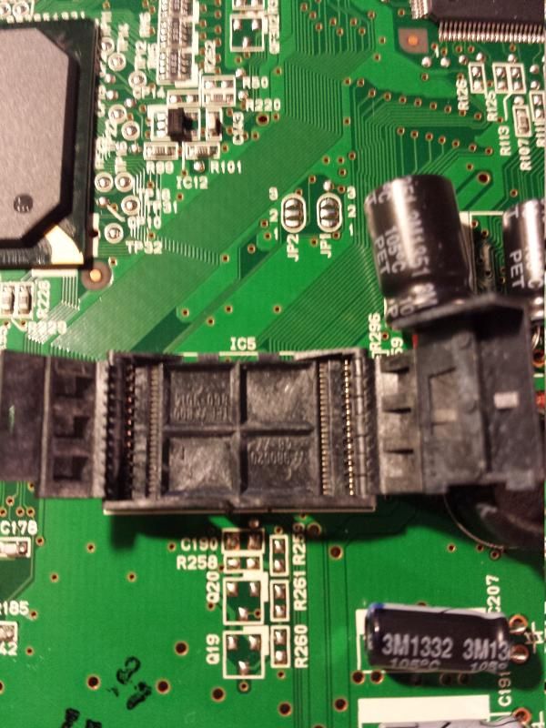
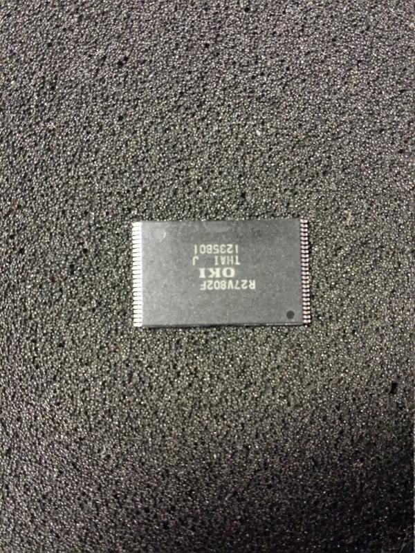
I thought this was going to be as easy as getting a new board and replacing it. Through extrapolating info I realized that I also needed to buy a PROM (or One time programmable Rom chip that is "plugged" into the main board.

I got the mainboard and the PROM directly from epson and the label on the PROM reads O.T.P ROM (Blank ROM) I looked extensively online for information regarding the replacement of the board and/or a service manual but it looks like epson is doing a great job in keeping this info hermetically unavailable.

I guess that nonetheless my questions are basic and might get answered here. (They all refer to the pictures attached)

Question number 1)

How do you determine the direction of the chip? It would seem that it can fit in two possible ways. Text straight or text upside down. (Is the text a standard for indicating the positioning of the chip?

Question number 2)

The notion that this is either a blank rom or a one time programmable one leads me to believe that it has to be programmed. Is that so or is it possible that when I turn on the scanner the board it self takes care of "filling" the rom?

Question number 3) If uncertain about 2) is there any risk on turning on the scanner with the blank rom on?

Thank you very much in advance for your help!


Offline macboy

  • Super Contributor
  • ***
  • Posts: 2254
  • Country: ca
Re: A question about inserting a Blank ROM on a PCB
« Reply #1 on: November 20, 2014, 02:24:48 pm »
Pin 1 is typically marked with a dot. But there are dots in opposite corners of you device. Pin 1 should be the upper left corner, looking at the device so the text is readable. That dot is more prominent and this is typical for this package.

The socket should be marked for pin 1 somewhere, again maybe something as simple as a dot or tick. Don't forget to look at the socket lid too. If not, the the silkscreen (white) on the PCB should indicate pin 1 with a dot, tick, "1", etc.  If not, then you may need to deduce pin 1 from the connections to the chip, looking for ground and power (ground is the large solid copper areas on the PCB), and comparing to the datasheet http://search.datasheetcatalog.net/key/R27V802

Epson would not have shipped a blank device, and in any case, you will not damage the scanner by using a blank device. It just won't work of course.
 

Offline Richard Crowley

  • Super Contributor
  • ***
  • Posts: 4317
  • Country: us
  • KJ7YLK
Re: A question about inserting a Blank ROM on a PCB
« Reply #2 on: November 20, 2014, 02:54:51 pm »
As macboy says, it is unlikely that they sold you a blank ROM.  And that more prominent mark is almost certainly the pin-1 mark.
Note that inserting the chip backwards is definitely NOT recommended, and quite likely to ruin the chip, so be careful.

Are there any marks on the board that may indicate pin-1?  We can't see under the "wings" that are open in your photo.
There may also be some indication on the BACK side of the board. Typically the pin-1 pad is a different shape than the others.
For example the pin-1 pad may be square while the others are oval-shape, etc.
 

Offline lleiroTopic starter

  • Newbie
  • Posts: 3
Re: A question about inserting a Blank ROM on a PCB
« Reply #3 on: November 20, 2014, 08:08:50 pm »
Thanks a lot guys!!! I believe I have found both of the markers you suggested but better safe than sorry:

When you flip the PROM the dot is only on one corner:

Top:

Bottom:

Now the plastic socket seems inconclusive, However there is an arrow on the board that is only on one corner as well.


This scheme would be consistent with the overall text direction which varies but remains consistent with the old board that has a soldered chip instead.

So... arrow with single dot?

Thanks again!


Offline marshallh

  • Supporter
  • ****
  • Posts: 1462
  • Country: us
    • retroactive
Re: A question about inserting a Blank ROM on a PCB
« Reply #4 on: November 20, 2014, 08:26:07 pm »
Yes, that seems to be correct. Have at it!
Verilog tips
BGA soldering intro

11:37 <@ktemkin> c4757p: marshall has transcended communications media
11:37 <@ktemkin> He speaks protocols directly.
 

Offline lleiroTopic starter

  • Newbie
  • Posts: 3
Re: A question about inserting a Blank ROM on a PCB
« Reply #5 on: November 21, 2014, 12:50:26 am »
A big thanks to all of you!

After 3 years I put the parts together and is working great!

 :-+
 

Offline chickenHeadKnob

  • Super Contributor
  • ***
  • Posts: 1055
  • Country: ca
Re: A question about inserting a Blank ROM on a PCB
« Reply #6 on: November 21, 2014, 07:25:22 am »
Well it is too late now to help, but I do one more thing to verify where pin one on the socket is if I am working on an unknown board and I have even the slightest doubt about screwing up, as in these cases it is not an option. What I do is look up the data sheet for the device and see which are the power and ground pins. Then I look on the board to see if I can tell how power and ground is routed to the socket. Often this can be easy, but on some  multilayer pcb may be difficult. You can double verify by powering up the board with an empty socket and  (carefully!) check which pins have power. What is good about doing it this way is that it provides an independent physical confirmation to the socket markings.

 I can't recall the last time when I had doubts about a chip orientation, but with unknown cabling between units  I always do this physical check. It has saved me much grief even if it appears a bit anal retentive/compulsive disorder. Consider the problem with ribbon cable connectors, the connectors may be keyed but sometimes are plugged into header which don't enforce the key or the cable can go into the keyed connector from either side when the cable is fabricated - they are not the same cable! Dave encountered that hazzard in one of his older videos when he demo'ed the Dangerous Prototypes Bus Pirate and wanted to test a small character LCD that had the old style 14 pin double row header connection.
 

Offline Kjelt

  • Super Contributor
  • ***
  • Posts: 6460
  • Country: nl
Re: A question about inserting a Blank ROM on a PCB
« Reply #7 on: November 21, 2014, 08:01:53 am »
@lleiro another tip for next time, the way you put the chip on the antistatic (black) foam that is 100% the way to do it  :-+
On the next pictures however you put it on bubblewrap plastick notorious for static electricity that could damage your device.  :(
Good work on fixing it  :clap:


Share me

Digg  Facebook  SlashDot  Delicious  Technorati  Twitter  Google  Yahoo
Smf