I was wondering if I could gather some thoughts on what would normally be a fairly simple circuit if not for some rather difficult complicating factors. The circuit so far is here:
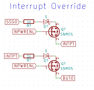
The basic idea is that when NPWRENL is high we essentially connect one line (SSS0) to a shared interrupt line (INTPT), and then that interrupt line (INTPT) to one side of a button (BUT0). The other side of the button is connected to ground. When we press the button with NPWRENL high, both lines are driven low. Note that current only has to flow one way. Unfortunately there are some complicating factors. These are:
- The particular bit of this circuit governs the interaction between an MCU (SAM4S), CPLD (Max V) and one button in a deep sleep mode. So power use is a major issue.
- In the deep sleep mode, the MCU is powered, but is in backup mode (essentially an ultra-low power mode for the SAM4S MCU) in which it can still output signals, and can only be woken via certain pins.
- In deep sleep mode, the CPLD is unpowered, having had its power removed by a pair of P-channel MOSFETs (also driven by NPWRENL at the gate). I could add a N-channel MOSEFT at ground too if it helps.
- NPWRENL will be greater than 3V via a 47k pullup when we are in deep sleep mode, or connected directly to ground when we are not.
- INTPT is a line read by the MCU when there is an interrupt state. The MCU pulls it high, and any device that wants to talk to the MCU pulls it low. INTPT goes to an external header and could be connected to absolutely *anything*, and such a device may signal a wakeup by driving the line low. It is also connected to the CPLD. I would like INTPT to rouse the MCU out of deep sleep mode.
- INTPT is connected to a MCU pin that cannot wake the MCU from backup mode, so I am trying to hook it up to a pin that can, but only in deep sleep mode (top part of the circuit). SSS0 was selected as the best option for now. Every single pin that can wake has a tradeoff. I can change the pin if it gives me too many problems.
- When outside of deep sleep mode, SSS0 has a completely different purpose- it is essentially a slave select line for SPI communication. Whatever I come up with, it needs to continue to function when not in deep sleep mode. SSS0 is connected to both the MCU and CPLD.
- I want the button to generate an interrupt (drive INTPT low), but only when in deep sleep mode. This is the reason for the lower part of the circuit. By connecting to BUT0, when the button is pressed, INTP will be shorted to ground.
- BUT0 is connected to the CPLD, but not the MCU. It is normally read via the CPLD, which will be unpowered in deep sleep mode.
- This part of the circuit still needs to operate using low power, even when not in deep sleep mode. The reason is that this mode is just the lowest of a few sleep modes.
- NPWRENL can be as high as 5.5V briefly, which will damage the MCU or CPLD if connected directly. Thus I need to keep it connected to gates or add another MOSFET to get around it.
- I am concerned the CPLD might try to pinch power that it finds on its I/O lines, which is important due to this being used to implement an ultra-low-power deep sleep mode. INTP, SSS0, and BUT0 *all* reach CPLD I/O pins. The MAX V handbook strongly suggests (under s4 "Hot-Socketing Specifications) that signal pins won't drive the power supplies. However I went and measured it anyway, and if there are any pullups connected to I/Os it seems to feed off of them (current was shown exiting ground pins). This will probably complicate the eventual solution.
- There does also exist a PWRENL directly connected to the MCU if needed (it drives an NMOS which controls NPWRENL).
I do have some flexibility to change my approach if needed to solve the problem. Beyond a certain point (about 6uA) it makes sense to just leave the CPLD connected the whole time and wear the power loss. However, the MCU can (apparently) get down to 1uA, and it would be nice to get close to that.
Or, perhaps there already exists a low power part that you can attach near a battery that you can signal to shut off power, and it sits and waits until you ground a certain input pin before it enables it again. I have a reset supervisor watching the battery voltage and switching a PMOS to isolate the battery if the voltage is too low. I could instead focus on that part of the circuit instead. There is a mild downside to that approach with respect to the MCU, but I can work around it, especially if it provides a superior solution on the power front.
Input most welcome.


