Author Topic: Help me understand these schematics!  (Read 10718 times)

0 Members and 1 Guest are viewing this topic.

Offline PoshTopic starter

  • Contributor
  • Posts: 15
  • Country: au
Help me understand these schematics!
« on: January 19, 2015, 02:05:42 pm »
Hello, I've come across some circuitry within some schematics that I do not understand. The schematics are both of brush less DC motor speed controllers, produced for the remote control hobby market. I have highlighted the offending circuitry.

Schematic 1:


Schematic 2:


I apologise for the poor paint skills.. Drawing straight lines on my laptop's touch pad is quite an art.  ::)
The offending circuitry (bottom left) in both images seem to be similar in function, as they both involve the external signal input line. My best guess as to the function of the top bits (highlighted) of both circuits is that it interfaces some of the unused pins of the micro controller for some reason.
I have seen schematics such as this one(warning: download link) that do not use this circuitry. So what does this circuitry do? And why is it not necessary on the other linked schematic?
Thanks in advance for any input!
 

Offline RR

  • Contributor
  • Posts: 30
  • Country: cz
Re: Help me understand these schematics!
« Reply #1 on: January 19, 2015, 02:35:18 pm »
SCH1:
top box- resistor to limit current and clamping diode to limit max voltage so it will not destroy input pin
bottom box- from signal_in thats series resistor and cap to gnd so thats make low pass RC filter
                  - from +UB thats voltage divider with decoupling cap

SCH2:
again just voltage dividers to feed AD converter in mcu, from the connector there is again low pass then weak pull up. Not sure whats the purpose of D6 there
 

Offline rob77

  • Super Contributor
  • ***
  • Posts: 2085
  • Country: sk
Re: Help me understand these schematics!
« Reply #2 on: January 19, 2015, 03:04:30 pm »
i would bet on the following:

schematic1:
top -  zener/reference connected to one of the ADC pins - to provide a known voltage to the micro's ADC input
bottom - input low pass + UB voltage divider as RR said, but the UB divider is to measure the battery voltage (in conjuction with the zener/reference at the top).

schematic2:
bridge for temperature measurement - connected to ADC inputs ADC1/ADC2
+ some input stuff on bottom left
 

Offline Richard Crowley

  • Super Contributor
  • ***
  • Posts: 4317
  • Country: us
  • KJ7YLK
Re: Help me understand these schematics!
« Reply #3 on: January 19, 2015, 03:16:41 pm »
In Schematic 1:
D1 may be used as a temperature-sensor to measure ambient (or heat-sink) temperature, depending on what it looks like and where it is. And R16 is it's pull-up resistor.
R24/C8 appears to be a noise filter to keep high frequency noise out of the control input line.
R20/R21 appear to be a voltage divider to allow the micro-controller to measure the battery voltage (if that is what "UB" is?)  And C7 is a filter cap to keep noise out of that node.

In Schenatic 2:
R1/R8 appear to be a voltage divider to allow the microcontroller to measure the battery voltage., and C4 is a noise fllter.
And likewise, R23/R24 are either a voltage divider to measure the 5V bus, or R24 may be an operational adjustment for something
Dunno what the up and down arrow symbol means in this context?  Really need the larger picture (the context)  to understand the schematic.
Since JP1 is not labeled, we can only guess that R7/C1 is another noise low-pass filter for an unidentified incoming signal. With R25 as a pull-up.
Most mysterious is D6 which is almost impossible to guess without some context of what function JP1 plays in the circuit.

Since most microcontrollers (like the ones shown in your schematics) have internal voltage-references, I do not think that any of those external components in either circuit are any kind of reference circuit.  I think they all play some more important external function.  Photos of the boards would be very helpful clues to arrive at better conclusions.
« Last Edit: January 19, 2015, 03:20:59 pm by Richard Crowley »
 

Offline rob77

  • Super Contributor
  • ***
  • Posts: 2085
  • Country: sk
Re: Help me understand these schematics!
« Reply #4 on: January 19, 2015, 03:27:00 pm »
schematic2 : R24 is definitely a thermistor for measuring temperature - i think for thermal shutdown.
 

Offline Richard Crowley

  • Super Contributor
  • ***
  • Posts: 4317
  • Country: us
  • KJ7YLK
Re: Help me understand these schematics!
« Reply #5 on: January 19, 2015, 03:33:51 pm »
Yes, I agree with rob77 that R24 is likely a thermistor or an RTD (resistance temperature detector)

« Last Edit: January 19, 2015, 03:37:21 pm by Richard Crowley »
 

Offline PoshTopic starter

  • Contributor
  • Posts: 15
  • Country: au
Re: Help me understand these schematics!
« Reply #6 on: January 20, 2015, 03:56:59 am »
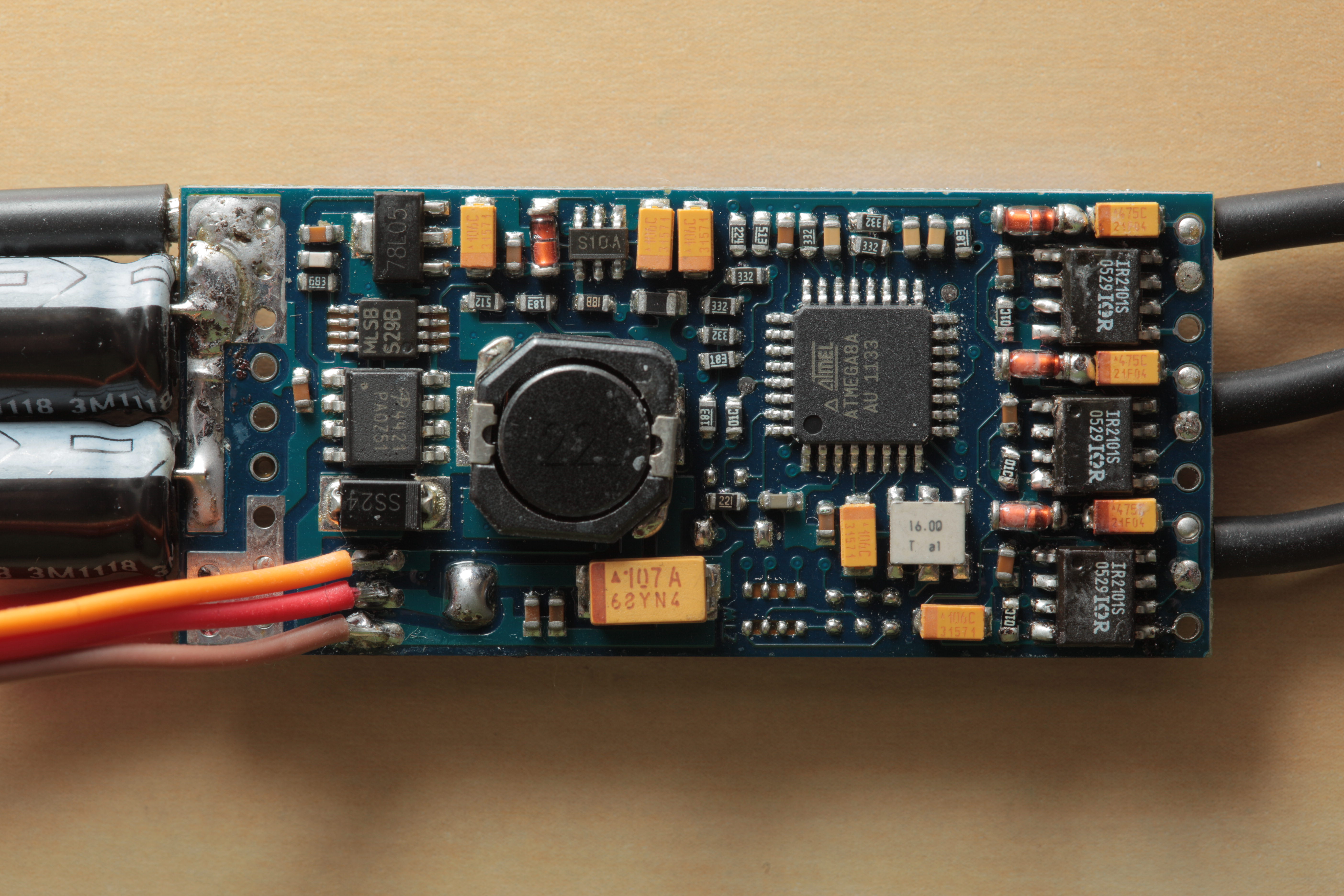
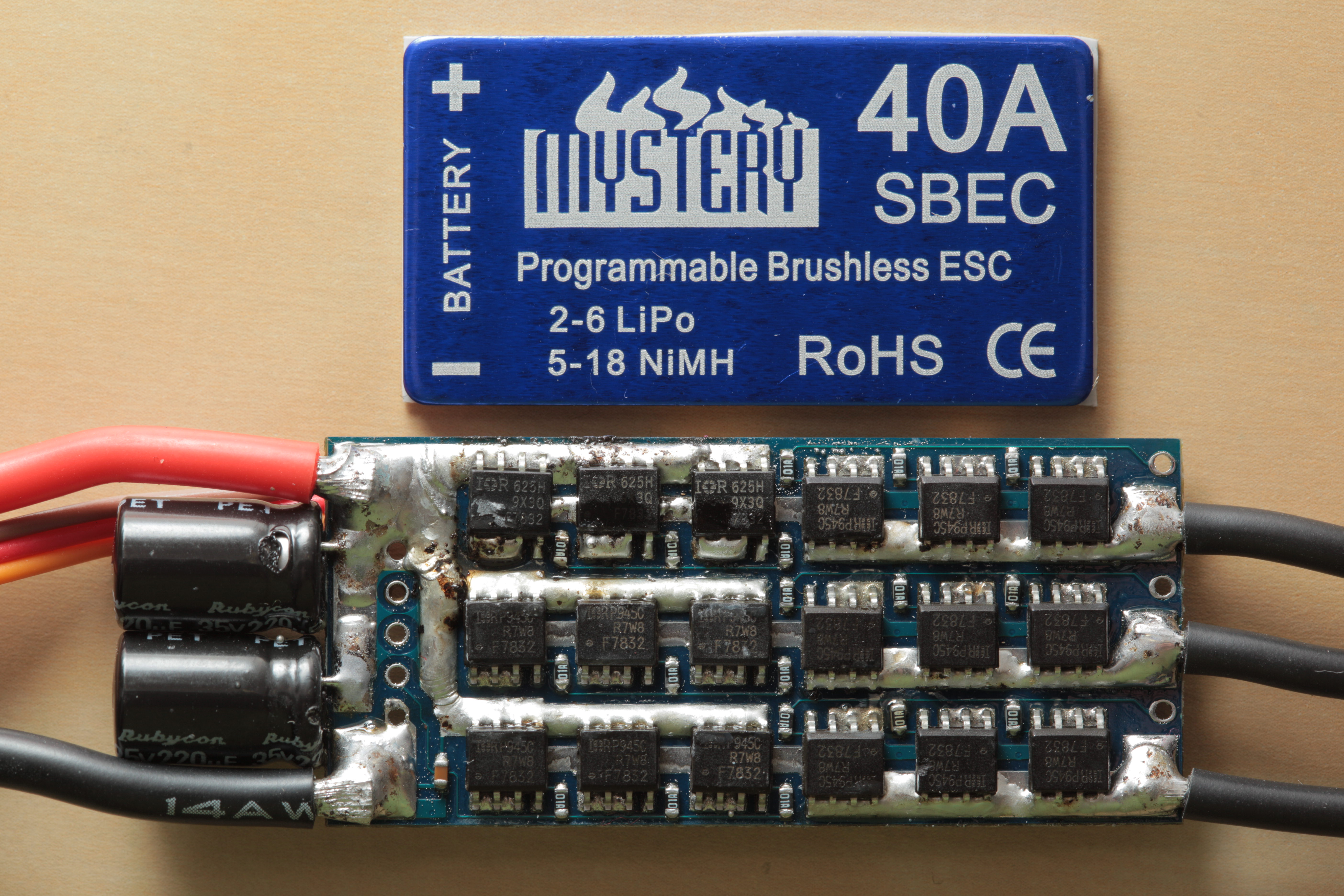
Thanks for the help guys, unfortunately I do not own these boards, I was just using the schematics for some research, and so I don't have any pictures. I did find these images on Google however:

Mystery 30A ESC (schematic 1)
Front:

Back: (apologies, I couldn't find a better picture)


Mystery 40A ESC (schematic 2)
Front:

Back:


I can't guarantee these match the schematics, as there seems to be both old and new versions of these speed controllers. JP1 is a connector, identical to the connector labeled "BEC" in the first schematic, which connects to an RC receiver for throttle signals etc. The RC receiver runs off of the 5v supplied by the regulators of the speed controller. These connectors are from top to bottom, RC input (throttle), 5v and ground.
« Last Edit: January 20, 2015, 03:49:19 pm by Posh »
 

Offline RR

  • Contributor
  • Posts: 30
  • Country: cz
Re: Help me understand these schematics!
« Reply #7 on: January 20, 2015, 01:27:07 pm »
its one of the RC models controllers so input signal should be 5V pwm right?

first front pic not working for me

SCH2:
looks like D6 and that pull up R25 is not populated so its just low pass
R1/R8 is definitely voltage divider for battery measure
R23/24-R24 should be thermistor (between inductor and that two tantalum caps on top)
 

Offline PoshTopic starter

  • Contributor
  • Posts: 15
  • Country: au
Re: Help me understand these schematics!
« Reply #8 on: January 20, 2015, 03:50:35 pm »
its one of the RC models controllers so input signal should be 5V pwm right?

Yes, I believe the input signals are pwm. I re uploaded the first image to a different site, can you see it now?
 

Offline dannyf

  • Super Contributor
  • ***
  • Posts: 8221
  • Country: 00
Re: Help me understand these schematics!
« Reply #9 on: January 20, 2015, 03:52:49 pm »
Both inputs go through a low pass filter.

It is interesting that they didn't adc that input. Instead, they seem to use PCINTx to detect the input width.
================================
https://dannyelectronics.wordpress.com/
 

Offline Richard Crowley

  • Super Contributor
  • ***
  • Posts: 4317
  • Country: us
  • KJ7YLK
Re: Help me understand these schematics!
« Reply #10 on: January 20, 2015, 04:26:28 pm »
Both inputs go through a low pass filter.

It is interesting that they didn't adc that input. Instead, they seem to use PCINTx to detect the input width.
But the input is digital (PWM) so you don't need an analog input.
The input filters are likely to keep that HF, high-current motor switching noise out of the inputs.


Share me

Digg  Facebook  SlashDot  Delicious  Technorati  Twitter  Google  Yahoo
Smf