Author Topic: Need help with some RF basics (and sources)  (Read 10653 times)

0 Members and 1 Guest are viewing this topic.

Offline poorchavaTopic starter

  • Super Contributor
  • ***
  • Posts: 1672
  • Country: pl
  • Troll Cave Electronics!
Need help with some RF basics (and sources)
« on: June 08, 2014, 05:21:35 pm »
I decided to have a go at RF voodoo. Partially because of work, partially because of my own interest. I think I will be implementing a transceiver based on TI CC110L chip to communicate in 433MHz ISM band.

They have a nice reference schematic in the datasheet:

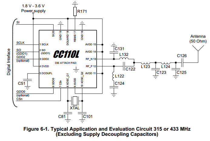
Values of the passives are:
C122=3.9p
C123=8.2p
C124=220p
C125=5.6p
C126=220p
L122=27n
L123=22n
L124=27n
L132=27n

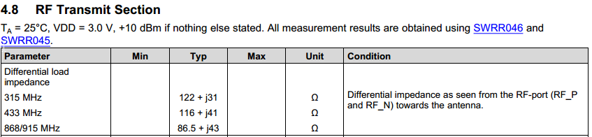
The only piece of information I've found about CC110L impedance is:


The questions I have so far are:
1) chip's RF port impedance
Datasheet says in 'RF Transmit' section that differential impedance as seen from RF port towards the antenna is 116+j41 ohms. How am I supposed to understand that? Is that the impedance of internal LNA? (PA outputs and LNA inputs are tied together). If so, then what's the impedance of the PA in transmit mode?

They state, that C131, L132, C122 and L122 for a balun that also mathes the differential impedance of the chip to 50 Ohm antenna, and other components (L123, L124, C123 and C125 are a filter). So how did they calculate the balun component values? I've calculated all the complex impedances of all the components and then tried various variants in FreeMat, but simnply nothing adds up.

Also, most of the smith chart applications somehow omit the possibility of RF source hacing other impedance than 50+j0.

I'd be really grateful for any hints or sources that I could use, because I'm totally lost on this one.
I love the smell of FR4 in the morning!
 

Offline KJDS

  • Super Contributor
  • ***
  • Posts: 2442
  • Country: gb
    • my website holding page
Re: Need help with some RF basics (and sources)
« Reply #1 on: June 08, 2014, 05:35:06 pm »
Don't think of it as a source in the matching tool, think if it as the load that you want to match to 50ohms and then you can use the matching tool.

However, it's probably worth learning how to use a smith chart. It's a pain to learn, but I don't think you can do real RF without one

Offline poorchavaTopic starter

  • Super Contributor
  • ***
  • Posts: 1672
  • Country: pl
  • Troll Cave Electronics!
Re: Need help with some RF basics (and sources)
« Reply #2 on: June 08, 2014, 06:16:27 pm »
I know the basics of smith's chart, I mean how to plot impedances and admittances and so on. But i have no idea how to translate that into designing a matching lumped element balun.
I love the smell of FR4 in the morning!
 

Offline Fank1

  • Regular Contributor
  • *
  • Posts: 159
Re: Need help with some RF basics (and sources)
« Reply #3 on: June 08, 2014, 07:31:07 pm »
This probably won't help with the differential output, but google Smith V3.10.
 

Offline poorchavaTopic starter

  • Super Contributor
  • ***
  • Posts: 1672
  • Country: pl
  • Troll Cave Electronics!
Re: Need help with some RF basics (and sources)
« Reply #4 on: June 08, 2014, 08:11:18 pm »
I've seen this program. My problem is that I don't know how to apply the basics of impedance matching to the real situation where I have differential input and output on the same two pins  and I need to make a bidirectional matching to a 50 Ohm single ended antena.
I love the smell of FR4 in the morning!
 

Offline Rory

  • Frequent Contributor
  • **
  • Posts: 410
  • Country: us
Re: Need help with some RF basics (and sources)
« Reply #5 on: June 08, 2014, 08:59:16 pm »
You didn't say what C131 value is, datasheet says 3.9p.

C131 = C122 and L132 = L122.   L networks C131-L132 and C122-L122 are phase shifters. (C124 is just a DC blocker).  Usually done as +90 and -90 degree shifters. You can work out the phase shifts from the example.  Combined outputs are in phase.

Impedances for each differential output/phase shift network can be calculated separately then paralleled at the node where they join. This gives you the source impedance for the lowpass filter.

I use Smith 3.10 as well. 
 

Offline Rory

  • Frequent Contributor
  • **
  • Posts: 410
  • Country: us
Re: Need help with some RF basics (and sources)
« Reply #6 on: June 08, 2014, 09:05:46 pm »
Here's the patent for the phase shift balun used here:

http://www.freepatentsonline.com/6621370.html
 

Offline KJDS

  • Super Contributor
  • ***
  • Posts: 2442
  • Country: gb
    • my website holding page
Re: Need help with some RF basics (and sources)
« Reply #7 on: June 08, 2014, 09:30:20 pm »
Here's the patent for the phase shift balun used here:

http://www.freepatentsonline.com/6621370.html

That was patented in 2003? I'm sure that circuit configuration is older than I am.

Offline Rory

  • Frequent Contributor
  • **
  • Posts: 410
  • Country: us
Re: Need help with some RF basics (and sources)
« Reply #8 on: June 08, 2014, 09:48:31 pm »
Here's the patent for the phase shift balun used here:

http://www.freepatentsonline.com/6621370.html

That was patented in 2003? I'm sure that circuit configuration is older than I am.

For sure, LC phase shift networks are far from something new. As a balun, I don't know, I've seen the +90/-90 phasing networks done before but never in a balun. Had to research and think about it a bit before commenting here.

I think most of us have been conditioned to think of baluns as some kind of inductive device, because most of the published designs are broadband baluns ala W2FMI. So could a narrowband balun as described in the patent could be considered unique at the time it was patented?
 

Offline poorchavaTopic starter

  • Super Contributor
  • ***
  • Posts: 1672
  • Country: pl
  • Troll Cave Electronics!
Re: Need help with some RF basics (and sources)
« Reply #9 on: June 08, 2014, 11:42:33 pm »
You didn't say what C131 value is, datasheet says 3.9p.

C131 = C122 and L132 = L122.   L networks C131-L132 and C122-L122 are phase shifters. (C124 is just a DC blocker).  Usually done as +90 and -90 degree shifters. You can work out the phase shifts from the example.  Combined outputs are in phase.

Impedances for each differential output/phase shift network can be calculated separately then paralleled at the node where they join. This gives you the source impedance for the lowpass filter.

I use Smith 3.10 as well.

Ok, so I should calculate impedance for half of the balun separately. But how should i treat the chip impedance (116+j41). Common sense says, that since this is differential, the single ended impedance from each port to gnd will be 58+j20.5, can I calculate like that?
I love the smell of FR4 in the morning!
 

Offline DJ

  • Supporter
  • ****
  • Posts: 129
  • Country: us
Re: Need help with some RF basics (and sources)
« Reply #10 on: June 09, 2014, 12:20:31 am »
I did a TI zigbee board awhile back. Used a tdk balun designed for the cc2530 (2.4ghz, not 433 MHz)

www.ti.com/litv/pdf/swra378

Stuck pretty close to the reference layout and passed testing the first go-round.


TI has a pretty active rf forum. Use it.

See if there are any integrated parts like the tdk balun for your part.

Stick to the reference layout as much as possible.
 

Offline Rory

  • Frequent Contributor
  • **
  • Posts: 410
  • Country: us
Re: Need help with some RF basics (and sources)
« Reply #11 on: June 09, 2014, 01:23:23 am »

Ok, so I should calculate impedance for half of the balun separately. But how should i treat the chip impedance (116+j41). Common sense says, that since this is differential, the single ended impedance from each port to gnd will be 58+j20.5, can I calculate like that?
That's a good question.  Try it and see if the results fit with the components given in the example, i.e. the end result is close to 50+j0 ohms. 

I agree with DJ, you might want to go over to the TI forums and ask specific questions there. I hope they're more helpful than the Microchip forums.
 

Offline VK5RC

  • Supporter
  • ****
  • Posts: 2672
  • Country: au
Re: Need help with some RF basics (and sources)
« Reply #12 on: June 09, 2014, 10:46:53 am »
One comment raised was about the direction of the impedance match,  you only have to solve it one way,  a transmitter line works well as a receiving line
Whoah! Watch where that landed we might need it later.
 

Offline vk6zgo

  • Super Contributor
  • ***
  • Posts: 7679
  • Country: au
Re: Need help with some RF basics (and sources)
« Reply #13 on: June 09, 2014, 11:44:57 am »
Let's think about what you need to do:-

(1) You are trying to match a higher impedance balanced source to an unbalanced antenna  with an impedance of (ideally) 50 Ohms,resistive,so your antenna matching circuit must act as a balun,& as an impedance matching network.

(2)The output impedance of the device has a substantial Inductive reactive component,(116+j41 Ohms),& the matching circuit must convert that to a purely resistive impedance of 50+j0 Ohms  at the antenna.

Google "Conjugate Matching."
 

Offline G0HZU

  • Super Contributor
  • ***
  • Posts: 3156
  • Country: gb
Re: Need help with some RF basics (and sources)
« Reply #14 on: June 09, 2014, 04:10:28 pm »
Quote
1) chip's RF port impedance
Datasheet says in 'RF Transmit' section that differential impedance as seen from RF port towards the antenna is 116+j41 ohms. How am I supposed to understand that? Is that the impedance of internal LNA? (PA outputs and LNA inputs are tied together). If so, then what's the impedance of the PA in transmit mode?

I think the 116, j41 impedance is the diff impedance presented to the diff output pins of the device when looking through the external LC network towards the antenna. The 116, j41 figure appears to be what their dev PCB presented to the chip at 433MHz. In other words I think you are supposed to make sure that your external network provides something (fairly) similar after it is neatly and tightly laid out on the PCB.

Note: Even if you use their 0402 packaged component values you will have to use the SAME PCB layout and PCB material in order to replicate their results.

eg if you used physically larger parts (but same component values) and used a sloppy PCB layout then you won't be presenting the correct load impedance to the chip and the Tx performance will suffer.

The balun section is easy to design if you treat it as a separate section. I can attach an excel spreadsheet if that helps? eg if you were to try designing a balun for 50R to 116R at 433MHz the values for L and C are as below.


Input Freq   433   MHz

Input Z unbalanced   50   Ohms
Input Z balanced   116   Ohms

Inductance =    27.9927275   nH
Capacitance =    4.826332328   pF

Their LPF that they attach to this looks like a two section L match. However, I suspect that TI optimised the balun and LPF design once the LPF/Lmatch section was added so my spreadsheet values are slightly different to their datasheet.

Realistically though, you can't really go wrong at 433MHz as long as you use tiny SMD parts and a very tight PCB layout to minimise any parasitic effects introduced by the PCB layout.
« Last Edit: June 09, 2014, 04:14:33 pm by G0HZU »
 

Offline poorchavaTopic starter

  • Super Contributor
  • ***
  • Posts: 1672
  • Country: pl
  • Troll Cave Electronics!
Re: Need help with some RF basics (and sources)
« Reply #15 on: June 09, 2014, 04:20:49 pm »
Quote
1) chip's RF port impedance
Datasheet says in 'RF Transmit' section that differential impedance as seen from RF port towards the antenna is 116+j41 ohms. How am I supposed to understand that? Is that the impedance of internal LNA? (PA outputs and LNA inputs are tied together). If so, then what's the impedance of the PA in transmit mode?

I think the 116, j41 impedance is the diff impedance presented to the diff output pins of the device when looking through the external LC network towards the antenna. The 116, j41 figure appears to be what their dev PCB presented to the chip at 433MHz. In other words I think you are supposed to make sure that your external network provides something (fairly) similar after it is neatly and tightly laid out on the PCB.

Note: Even if you use their 0402 packaged component values you will have to use the SAME PCB layout and PCB material in order to replicate their results.

eg if you used physically larger parts (but same component values) and used a sloppy PCB layout then you won't be presenting the correct load impedance to the chip and the Tx performance will suffer.

The balun section is easy to design if you treat it as a separate section. I can attach an excel spreadsheet if that helps? eg if you were to try designing a balun for 50R to 116R at 433MHz the values for L and C are as below.


Input Freq   433   MHz

Input Z unbalanced   50   Ohms
Input Z balanced   116   Ohms

Inductance =    27.9927275   nH
Capacitance =    4.826332328   pF

Their LPF that they attach to this looks like a two section L match. However, I suspect that TI optimised the balun and LPF design once the LPF/Lmatch section was added so my spreadsheet values are slightly different to their datasheet.

Realistically though, you can't really go wrong at 433MHz as long as you use tiny SMD parts and a very tight PCB layout to minimise any parasitic effects introduced by the PCB layout.


I hit that one too, using the formula Zc=Zl=sqrt(Zs*Zl), it just bothered me that they used 3p9 instead of 4p7, but perhaps they accounted for parasitic pcb capacitance?

Anyway, does that mean that imaginary part of chip impedance should be omitted when designing a balun? What happens to that part? Should i compensate for it further in the matching network?
I love the smell of FR4 in the morning!


Offline poorchavaTopic starter

  • Super Contributor
  • ***
  • Posts: 1672
  • Country: pl
  • Troll Cave Electronics!
Re: Need help with some RF basics (and sources)
« Reply #17 on: June 09, 2014, 07:48:44 pm »
Thanks, i'll definitely read that :)
I love the smell of FR4 in the morning!
 

Offline KJDS

  • Super Contributor
  • ***
  • Posts: 2442
  • Country: gb
    • my website holding page
Re: Need help with some RF basics (and sources)
« Reply #18 on: June 09, 2014, 08:05:56 pm »
What is worth doing is putting the equations into excel and using RFSim99 or a matching program to check that you've got them right. If you understand the maths life is so much easier. It just takes a while to understand the maths.

Offline G0HZU

  • Super Contributor
  • ***
  • Posts: 3156
  • Country: gb
Re: Need help with some RF basics (and sources)
« Reply #19 on: June 09, 2014, 09:12:26 pm »
Quote
Anyway, does that mean that imaginary part of chip impedance should be omitted when designing a balun? What happens to that part? Should i compensate for it further in the matching network?

I think it depends how close you want to get to (presenting) the ideal load impedance to the device with your balun/filter network. However, there are other factors to take into account such as the PCB type/thickness and the layout. If I wanted to design the system to hit 116, j41 at 433MHz then I'd want to measure and create a 1 port model of the antenna and I'd do an EM simulation of the PCB layout and then optimise all the components  for best performance.

But in reality I probably wouldn't bother with the EM sim of the layout because this isn't really a critical design in that the circuit is going to have a very low loaded Q and will be fairly predictable as long as you use small SMD parts and have a decent PCB layout. But you do need to think about the impedance of your antenna because it is unlikely to be 50, j0 at 433MHz. So this will screw up the load impedance presented to the chip unless you factor in the actual antenna impedance. If it has a VSWR of 2:1 at 433MHz and you designed for 1:1 then you will no longer be presenting the ideal load impedance to the chip the moment you swap the 50R dummy load for your real antenna.

I've not used this chip before but I suspect that the most important aspects of this part of the design are to keep a tight and symmetrical PCB layout for the balun components and to add as much filtering after it to meet your requirements. The chip itself will probably be very rich in odd order harmonics so you need to decide if the filtering is adequate for your needs.

« Last Edit: June 09, 2014, 09:17:15 pm by G0HZU »
 

Offline poorchavaTopic starter

  • Super Contributor
  • ***
  • Posts: 1672
  • Country: pl
  • Troll Cave Electronics!
Re: Need help with some RF basics (and sources)
« Reply #20 on: June 10, 2014, 11:35:41 am »
I have made following calculations:
-divided input impedance of 116+j41 by 2, assuming that either input has 58+j20.5 to ground.
-calculated impedance for each branch of of the balun separately
-calculated equivalent impedance for parallel connection of both branches
-added L123 in series, C123 in parallel, L124 in series, C125 in parallel

this gives me the result of roughly 64-j0.7 ohms, and as far as i understand, this is the impedance, that signals coming from the antenna see, when entering the circuit. Can this be correct? Calculating complex reflection coefficient (zin, is the 64-j0.7 calcualted before, zant is 50+j0) as (zin-zant)/(zin+zant) gives the result of 0.1242-j0.0057, and VSWR calculated as (1+mag(refl_coeff))/(1-mag(refl_coeff)) comes out as 1.2840.

Can this be considered a roughly good math to a 50 ohm antenna?
I love the smell of FR4 in the morning!
 

Offline Rory

  • Frequent Contributor
  • **
  • Posts: 410
  • Country: us
Re: Need help with some RF basics (and sources)
« Reply #21 on: June 10, 2014, 12:33:36 pm »
1.28:1 is an entirely acceptable VSWR. 

Take into consideration also, that the antenna itself will seldom have an exact 50 ohm impedance. Add to this that in this application the antenna may come in close proximity to other objects which will affect its resonant frequency and impedance characteristics, so the actual Z is virtually unknown. 


Offline KJDS

  • Super Contributor
  • ***
  • Posts: 2442
  • Country: gb
    • my website holding page
Re: Need help with some RF basics (and sources)
« Reply #22 on: June 10, 2014, 12:54:53 pm »
I have made following calculations:
-divided input impedance of 116+j41 by 2, assuming that either input has 58+j20.5 to ground.
-calculated impedance for each branch of of the balun separately
-calculated equivalent impedance for parallel connection of both branches
-added L123 in series, C123 in parallel, L124 in series, C125 in parallel

this gives me the result of roughly 64-j0.7 ohms, and as far as i understand, this is the impedance, that signals coming from the antenna see, when entering the circuit. Can this be correct? Calculating complex reflection coefficient (zin, is the 64-j0.7 calcualted before, zant is 50+j0) as (zin-zant)/(zin+zant) gives the result of 0.1242-j0.0057, and VSWR calculated as (1+mag(refl_coeff))/(1-mag(refl_coeff)) comes out as 1.2840.

Can this be considered a roughly good math to a 50 ohm antenna?

That's a reasonable starting place. Now add in a little inductance for any shunt component and a little transmission line for the traces between components. Then look at the inductor data sheet and find the self resonant frequency of the inductor. Calculate the capacitance in parallel with the inductor required to give this resonance and add that to the model, then you'll have something much closer to reality. Whether those extra steps are worth the effort is entirely case dependent.

Offline G0HZU

  • Super Contributor
  • ***
  • Posts: 3156
  • Country: gb
Re: Need help with some RF basics (and sources)
« Reply #23 on: June 10, 2014, 11:25:11 pm »
Quote
and as far as i understand, this is the impedance, that signals coming from the antenna see, when entering the circuit. Can this be correct?
No. I don't think you are reading the datasheet correctly (or listening to me either)

I'm pretty sure that the 116 j41 impedance refers to the diff impedance looking back from the device to the antenna via the balun/filter network. The datasheet doesn't tell you the impedance of the chip's port pins in tx mode.

i.e. I think you are supposed to present 'something in the ballpark of'  this 116 j41 impedance to the chip. You seem to be doing it backwards because you think the chip has this impedance as its source impedance.

Note: The 116 j41 impedance may be a compromise 'target' for your network to achieve such that you get a good compromise between Tx performance (looking into 116, j41)  and the receive performance when signals come back from the antenna into the receive part of the chip.

If you want to Tx at 433MHz then why don't you just copy their circuit layout and use the same 0402 parts? As long as you use tight tolerance parts and have a PCB material and layout that mimics the app note then you will be fine. This assumes you will use an antenna that is reasonably close to 50R and you aren't too fussed about harmonic suppression levels.

« Last Edit: June 10, 2014, 11:41:44 pm by G0HZU »
 

Offline poorchavaTopic starter

  • Super Contributor
  • ***
  • Posts: 1672
  • Country: pl
  • Troll Cave Electronics!
Re: Need help with some RF basics (and sources)
« Reply #24 on: June 10, 2014, 11:52:17 pm »
I can copy the reference design for sure, but I want to understand how this works and how it was calculated.

It kind of seems to me, that since the PA and the LNA chare the same ports and they are connected to the same matching network which works both ways, then the PA would need to have the same impedance as the LNA or there would be dofferent (worse) power transfer either during Rx or Tx. If what you're saying is true, than 116+j41 should be the impedance of matching network + antenna, and to have optimal power transfer between entanna and then chip, the chip impedance would have to be a complex conjugate of the matching network + antenna, so 116-j41. I will see tomorrow, if this matches the components used (I wrote at work a small FreeMat script that speeds up the calculations)

As for EM simulation I do not have access to such software, unless you can recommend a good free program that does it.

As for PCB, the reference board from TI is 2-layer and so will be mine, but the Er of the laminate will be  different for sure. This is another problem, since assuming laminate Er of about ~4, a 50Ohm transmission line on a 1.6mm thick double sided board would be ~3mm wide, which may be a problem for practical implementation.
I love the smell of FR4 in the morning!


Share me

Digg  Facebook  SlashDot  Delicious  Technorati  Twitter  Google  Yahoo
Smf