Author Topic: Understanding a diagram  (Read 4501 times)

0 Members and 1 Guest are viewing this topic.

Offline bitmanTopic starter

  • Supporter
  • ****
  • Posts: 299
  • Country: us
  • Open Source Guy jabbing with Electronics
Understanding a diagram
« on: April 29, 2017, 07:43:02 pm »
Again a Q from the newbie. I'm trying to understand crystal circuits and get to use them. I mentioned on another thread, that so far I've had little success getting them to work.

I think it's because I don't understand how to read the basic/beginner diagram, one of which I've attached here. All I see is "output" and ground. Where/how does this get input voltage to work on?   I'm not sure how to connect this. I have a CK input on a CD4017 that I'm attempting to use - and I get where I need to connect the input - but how does voltage get to this circuit in the first place??
 

Offline retrolefty

  • Super Contributor
  • ***
  • Posts: 1648
  • Country: us
  • measurement changes behavior
Re: Understanding a diagram
« Reply #1 on: April 29, 2017, 07:51:32 pm »
Quote
but how does voltage get to this circuit in the first place??

 The triangle figure is a digital gate circuit. It isn't shown but that gate will have a Vcc voltage (usually 5v or 3.3v) and ground applied to it also. That is enough to start generating random circuit noise. The rest of the circuit shown implement DC bias for the gate and a low-pass filtered AC feedback signal sent through the crystal which will force the gate to oscillate at the crystal's frequency.

 
The following users thanked this post: bitman

Offline bitmanTopic starter

  • Supporter
  • ****
  • Posts: 299
  • Country: us
  • Open Source Guy jabbing with Electronics
Re: Understanding a diagram
« Reply #2 on: April 29, 2017, 08:15:20 pm »
Quote
but how does voltage get to this circuit in the first place??

 The triangle figure is a digital gate circuit. It isn't shown but that gate will have a Vcc voltage (usually 5v or 3.3v) and ground applied to it also. That is enough to start generating random circuit noise. The rest of the circuit shown implement DC bias for the gate and a low-pass filtered AC feedback signal sent through the crystal which will force the gate to oscillate at the crystal's frequency.
Is that what's meant by having power/ground connected like this image: http://www.eleccircuit.com/wp-content/uploads/2007/08/pulse-generator-oscillator-32768khz-by-watch-crystal.jpg?? I could not make heads or tails out of it.
 

Offline theatrus

  • Frequent Contributor
  • **
  • Posts: 352
  • Country: us
Re: Understanding a diagram
« Reply #3 on: April 29, 2017, 08:21:38 pm »

Is that what's meant by having power/ground connected like this image: http://www.eleccircuit.com/wp-content/uploads/2007/08/pulse-generator-oscillator-32768khz-by-watch-crystal.jpg?? I could not make heads or tails out of it.

Correct. These shortcuts in schematics also exist with op-amps, where there is implicitly a supply voltage.
Software by day, hardware by night; blueAcro.com
 

Offline rdl

  • Super Contributor
  • ***
  • Posts: 3667
  • Country: us
Re: Understanding a diagram
« Reply #4 on: April 29, 2017, 09:53:50 pm »
Implied power connection is one of those schematic things that tend to confuse new people. Anytime you see that triangle symbol, usually for an op amp or logic gate, somewhere there is a power connection. It is often omitted for "clarity" or just out of laziness.

On a full schematic it does make sense, since there will usually be multiple op amps or gates in a single integrated circuit all sharing the same power pins, but the connection to the those pins may be shown somewhere far away from where the gates or op amps appear.

For a partial schematic or diagram, it's generally assumed that you just know that power is needed.
 
The following users thanked this post: bitman

Offline Brumby

  • Supporter
  • ****
  • Posts: 12297
  • Country: au
Re: Understanding a diagram
« Reply #5 on: April 30, 2017, 12:41:31 am »
The triangle is an inverter, as it has the little circle on the output.  A 4007++ 4069 or 7404 IC has six of these in the one package - and looks like this:


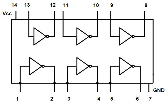
You see the Vcc and GND pins for the whole package, which powers all six inverters.

These power pins are often omitted in the body of a schematic, since each of the gates can be placed in different areas of the circuit.  In a full schematic, they can appear off to one side in a little symbol which appears to be nowhere special and doing nothing at all.  The trick is to understand how things are labelled.

Let's say you had a 4007++ 4069 IC in a circuit and the chip was labelled IC3.  Each of the six triangular symbols are then placed on the schematic (and they could be all over the place) but they will be labelled IC3a, IC3b, IC3c, IC3d, IC3e and IC3f - showing they are all in the single package.  There will may** also be the abovementioned symbol off to one side labelled IC3 which will only have the Vcc and GND pins shown.

Once you get the hang of it, this convention makes reading schematics a whole lot easier.

** EDIT: Where a circuit is powered from a single supply that is compatible with the IC, this might not be included - but, even so, these pins will need to be connected to power and ground.

++ EDIT 2:  :palm:
« Last Edit: April 30, 2017, 02:05:55 am by Brumby »
 

Offline rdl

  • Super Contributor
  • ***
  • Posts: 3667
  • Country: us
Re: Understanding a diagram
« Reply #6 on: April 30, 2017, 01:00:27 am »
Quote
A 4007 IC has six of these in the one package - and looks like this:

Well, only if it's actually a 4069...
 

Offline Brumby

  • Supporter
  • ****
  • Posts: 12297
  • Country: au
Re: Understanding a diagram
« Reply #7 on: April 30, 2017, 02:01:41 am »
 :palm:

It was a long night.  I need more caffeine.....
 

Online Zero999

  • Super Contributor
  • ***
  • Posts: 19492
  • Country: gb
  • 0999
Re: Understanding a diagram
« Reply #8 on: April 30, 2017, 09:02:55 am »
Note that the circuit is supposed to be made with a CMOS gate, not TTL. The old 7404 or 74LS04 are TTL and are unsuitable for this circuit. Go for the 74HC04, preferably the 74HCU04, which is unbuffered, therefore has less gain and is more likely to be stable.

It is possible to build a crystal oscillator with TTL but it's slightly different.

You can buy an IC dedicated to this task: the 74LVC1GX04. The only downside for a beginner is the small package.
http://assets.nexperia.com/documents/data-sheet/74LVC1GX04.pdf
« Last Edit: April 30, 2017, 09:09:48 am by Hero999 »
 

Offline Brumby

  • Supporter
  • ****
  • Posts: 12297
  • Country: au
Re: Understanding a diagram
« Reply #9 on: April 30, 2017, 02:25:31 pm »
I wasn't suggesting a 7400 series TTL chip would be suitable for the oscillator circuit.

The question was understanding the diagram.
 

Online Zero999

  • Super Contributor
  • ***
  • Posts: 19492
  • Country: gb
  • 0999
Re: Understanding a diagram
« Reply #10 on: April 30, 2017, 04:05:50 pm »
I wasn't suggesting a 7400 series TTL chip would be suitable for the oscillator circuit.

The question was understanding the diagram.
Yea I know.

The trouble is, the different types of logic gates can be confusing for a beginner. You mention the 7404 and may be fully aware that it's unsuitable for this circuit but someone who doesn't know the doesn't know the difference between the 74LS04 and 74HC04 might be tempted to use it, only to wonder why it doesn't work.
 

Offline Brumby

  • Supporter
  • ****
  • Posts: 12297
  • Country: au
Re: Understanding a diagram
« Reply #11 on: May 01, 2017, 02:29:43 am »
Fair enough.
 

Online T3sl4co1l

  • Super Contributor
  • ***
  • Posts: 21658
  • Country: us
  • Expert, Analog Electronics, PCB Layout, EMC
    • Seven Transistor Labs
Re: Understanding a diagram
« Reply #12 on: May 01, 2017, 04:37:56 am »
Unbuffered (CD4069U, 74HCU04) logic are preferred, because they are stable with DC feedback (the resistor from output to input).

The circuits usually work with regular (74HC04 or 14, 4069BE, etc.) logic too, though it's not recommended.

And yeah, the power pins aren't shown; the inverter is assumed to have +V and GND connected appropriately.  2 to 5V would be typical for 74HC, 5 to 15V for 4000 series.

Tim
Seven Transistor Labs, LLC
Electronic design, from concept to prototype.
Bringing a project to life?  Send me a message!


Share me

Digg  Facebook  SlashDot  Delicious  Technorati  Twitter  Google  Yahoo
Smf