OK, so the previous two examples are fine for micro-controller projects but the OP was interested in CP/M. For that you need RAM at low addresses because the TPA (i.e where programs are loaded) starts at 0x0100. Also you really need 64k of RAM if at all possible.
This all provides a bit of a problem, how do we have ROM at address 0 for the initial cold reset and RAM at address 0 when running CP/M? I should point out BTW that for the moment I'm thinking of CP/M 2.2 and below - CP/M 3.0 supported bank switching but it wasn't around the last time I built a machine to run CP/M so I need to go and have a look at how it works.
We need to introduce some ability to switch one bank between ROM & RAM - the following (totally from memory so untested) circuit should do the trick
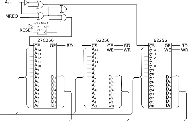
We now have two 32kx8 SRAM chips plus some additional gating with half a 74LS74 and a couple more OR gates. On reset the flip flop is cleared so the output will be low, this allows the chip select signal to pass to the EPROM. If a "1" is written to the flip-flop then the chip select will pass to the SRAM.
So, after a reset code in the ROM will run - as part of its initialisation it needs to copy some code up into addresses above 0x8000 and then jump to that code - the flip flop can then be switched to allow the whole 64k to be RAM.
I haven't shown how the clock input to the flip-flop is generated, so that can be considered an exercise for the reader  but it needs to be the result of combining a decoded I/O address and the processor WR signal. I'll try to find time for some posts covering I/O interfacing in the next day or two.
Hope these posts have been helpful.
Hi
Regarding the reset for the flip flop. Assuming that this is also connected to the processor reset pin, will the flip flop outputs always have settled before the processor is ready to read from memory for the first time ?
I guess the related question is can you also be sure that the flip flop will always have changed state fast enough for the first memory access after the bank switch request ?
I'm using a Z84C0010PEG clocked at 4MHz.
Thanks


