Author Topic: Z80 single board memory bank switching  (Read 44162 times)

0 Members and 1 Guest are viewing this topic.

Offline MrAureliusRTopic starter

  • Supporter
  • ****
  • Posts: 373
  • Country: ca
Z80 single board memory bank switching
« on: July 26, 2013, 06:18:38 pm »
Hi there.

So I've been fiddling with my Z80 for a while now, and I'm ready to kick things up a notch. My goal is to get the project to the point where I can 'talk' to my SBC over a serial terminal. In order to get there, I have to load the Z80 monitor into EEPROM (done) and then of course, hook up the SRAM, EEPROM, PIO/SIO/UART (depending on which I need), memory bank selector, and MAX232 (if needed, I can't remember if the UART/SIO/PIO puts out RS-232 voltages, I don't think they do).

My understanding of the theory is pretty good, it's just translating that into practical set-up that I'm finding difficult. There's a wealth of information on z80.info and I've been reading a LOT from that site, plus all the datasheets for the chips I'm using. And I've found a few great schematics for basic Z80 systems that are helping a lot.

However, I haven't been able to find much info on actually getting everything set up. My chips, of course, are not the exact same that are in the schematics. My INMOS 4K SRAM, for example, has only 4 I/O pins, and 12 address pins. This is completely different from most of the schematics, which typically show the 62256 for RAM and the 16C550 UARTs. Also, there's not a lot of info on implementing the PIO and SIO where needed.

I'm certainly not asking anyone to design this for me -- that would defeat the whole point. What I need help with is deciding which logic chips I need, and where. I'm trying to learn and build this on my own so I'm trying to take things in small bite sizes.

Attached is an annotated photo of what I have so far. Notice that nothing is hooked up yet, as I'm still researching how to do it. Currently all the Z80's data pins are going to ground, so it's just doing NOPs over and over, incrementing the address bus LEDs. This was set up just so I could make sure the Z80 I bought was in good working order. The reset circuit works, and I have a 555 creating a 12.5Hz clock signal currently. I also have a 20MHz oscillator for when things are working properly and I'm ready to push things to their speed limit. Of course the 555 is also adjustable which is great.

So, in order to hook up both the EEPROM and either the INMOS 4k or the Toshiba 64K SRAMs, should I simply connect the address lines to both chips and then have the 5th address line (in the case of the INMOS, which only has 4) going to the chip enable on the bigger chips? So that in theory, I can separate the SRAM and EEPROM into different memory space? This is the part where I get confused. Should I have A0-A3 going to the SRAM, then A4-A15 going to the EEPROM, with A4 also going to CE on the EEPROM? Or something like that? But then, how do I connected RD and MEMRQ? Do I use a logic gate so that when it goes above 4K on the address bus it switches to the SRAM?

Oh boy, I'm feeling a bit over my head, even though I know this should be really simple!

Any and all help is much appreciated! Even just a prod in the right direction ;)
--------------------------------------
Canadian hacker
 

Offline lapm

  • Frequent Contributor
  • **
  • Posts: 564
  • Country: fi
Re: Z80 single board memory bank switching
« Reply #1 on: July 26, 2013, 06:46:29 pm »
I think you have address line operation confused in your head. Z80 only has 64k Address space. What i would recommend, use two or three highest (A13, A14, A15) address line's to drive some sort of decoder to generate those chip select signals.

Not sure about other requirements Z80 might have since have newer used one on my own experiments.

Electronics, Linux, Programming, Science... im interested all of it...
 

Online PA0PBZ

  • Super Contributor
  • ***
  • Posts: 5127
  • Country: nl
Re: Z80 single board memory bank switching
« Reply #2 on: July 26, 2013, 06:49:41 pm »
(Trying not to give away the information, just pointing you in the right direction)
First you have to find out where the Z80 is going to read the first instruction after a reset, because that is where you want your program to start and I'm assuming where you want the EEPROM.
Secondly, all chips need their address lines to start with A0, otherwise your program will not run (if it is the EEPROM), or you will going to have a hard time to store/read the SRAM.
Not sure what you mean by only 4 I/O pins for the INMOS, but you will need 8 bits SRAM, so either use 2 chips or use the Toshiba.
A PIO is a Parallel Input/Output, so that's not going to do any RS232, and yes, you will need a MAX232.
You can do simple address 'decoding' by using the highest (A15) adddress line so you will split the addressable memory in 2 chunks of 32KB, one for the EEPROM and one for the SRAM.

Well, enough to look at and read for now I guess.
Keyboard error: Press F1 to continue.
 

Offline MrAureliusRTopic starter

  • Supporter
  • ****
  • Posts: 373
  • Country: ca
Re: Z80 single board memory bank switching
« Reply #3 on: July 26, 2013, 07:06:30 pm »
Okay, you're right, I had it a bit mixed up. I forgot that it's A15 you use for simple switching, you simply connect all the others on the bus and then switch A15 on or off to indicate which chip it's going to, basically.

Yeah, the INMOS has 12 address pins and 4 I/O pins. Attached is the datasheet. I think I will probably use the one of the Toshiba's, but either way they're both SRAM so they're good for low clock speed. Plus no refresh circuitry!

I think I'm starting to get it. The Toshiba's have an active low Output Enable pin, and then two Chip Enables, CE1 which is active low, and CE2 which is active high. I'm getting things a bit tangled up in my head again, though. There's also a R/W control pin. Would MREQ go to the low CE1, and then A15 to OE, and then tie CE2 high, attach both RD and WR to the R/W pin, but put the correct one (whichever one is asserted by active low) through an inverter? Is that making any sense?

[EDIT: OE is also active low, so I guess A15 would have to be inverted as well?]
--------------------------------------
Canadian hacker
 

Offline C

  • Super Contributor
  • ***
  • Posts: 1346
  • Country: us
Re: Z80 single board memory bank switching
« Reply #4 on: July 26, 2013, 08:05:01 pm »

This direct from Zilog could answer your questions

Z80 Family CPU User Manual - Zilog

the zilog manuals for the other Zilog chips are also good at explaining what is needed.

You do not have to start from scratch on software. You could copy the drivers for your SIO & PIO from a CPM-80 system that used these parts
CP/M Plus was fancier and was able to use more memory by bank switching

and there was turbo-dos that was a network of master & slave z80's
Using the ideas from turbo dos you could have your Z80 running CPM-80 programs while your SBC is acting like a terminal, disk dirve & printer.
For some of the turbo-dos slaves they were not much more then the Z80 & ram, the master did a big assist in the boot process. Your SBC might be able to do this also

C


Offline MrAureliusRTopic starter

  • Supporter
  • ****
  • Posts: 373
  • Country: ca
Re: Z80 single board memory bank switching
« Reply #5 on: July 26, 2013, 08:40:57 pm »

This direct from Zilog could answer your questions

Z80 Family CPU User Manual - Zilog

the zilog manuals for the other Zilog chips are also good at explaining what is needed.

You do not have to start from scratch on software. You could copy the drivers for your SIO & PIO from a CPM-80 system that used these parts
CP/M Plus was fancier and was able to use more memory by bank switching

and there was turbo-dos that was a network of master & slave z80's
Using the ideas from turbo dos you could have your Z80 running CPM-80 programs while your SBC is acting like a terminal, disk dirve & printer.
For some of the turbo-dos slaves they were not much more then the Z80 & ram, the master did a big assist in the boot process. Your SBC might be able to do this also

C

It's funny you should mention this -- my ultimate goal is to have CP/M 2 or 3 running. That's a bit of a ways away, I'd have to implement some sort of IDE interface. I know people have implemented IDE with a CompactFlash card slot, and that seems like a good idea. Even SD -- as I have a ton of SD cards lying around that'd be great.

I actually have a ROM of a Z80 monitor that this guy wrote for his single-board Z80 and he posted it online with a free license. So I compiled that and it compiled perfectly using the Z80 assembly compiler I have. Then I programmed that into the Atmel EEPROM I have on the board there. I've been trying to match his setup at least to some degree so I don't have to mess around with his code too much (as I don't know assembly well at all). I suppose I could if I had to... All his work can be found here.

In the beginning of his monitor code, he has a memory map to show how the memory space is divided between EEPROM and RAM. Does this look like a good starting point or should I maybe just jump to CP/M? I have the sources for CP/M, I just need to compile them, which shouldn't be too hard.

I suppose I need to figure out my physical setup first, before I get into software. Or is it the other way around?  :palm:
--------------------------------------
Canadian hacker
 

Offline grumpydoc

  • Super Contributor
  • ***
  • Posts: 2905
  • Country: gb
Re: Z80 single board memory bank switching
« Reply #6 on: July 26, 2013, 09:50:38 pm »
Not sure where to start. There are, however lots of schematics on the net for Z80 based systems. If you'll excuse the fact that I haven't played with one for 20 years (though there are increasing numbers accumulating in the parts bin so I really should put together a few simple systems sometime) here are some random thoughts.

CP/M is mildly tricky on a Z80 because it wants RAM at low addresses, unfortunately the Z80 pushes you towards ROM at low addresses because reset pushes 0000H into the program counter (actually that's pretty much all reset does) so you tend to want ROM there just after reset.

A minimal Z80 system can be built with a static RAM, a ROM and a few latches for a bit of memory mapped I/O. Depending on the RAM&ROM size you can construct a basic address decode with something like a 74LS138 (to decode 8 blocks of 8K) or half a 74LS156 (to decode 4 16K blocks). Using the former as an example you connect the top three address bits (A15, A14 and A13) to the A2, A1 and A0 inputs and MREQ to one of the active low enable inputs and that gives you 8 select signals which you can connect to the active low chip select lines on your EPROM and RAM. Obviously if you have one 8K EPROM and one 8K RAM you'll have six unused selects. These can be used for "memory mapped" I/O.

The INMOS RAM chip you mention is a 4kx4 so you need two of them one connected to D0 to D3 and one to D4 to D7 but really it's a lot simpler to find a 6264 somewhere.

True bank switching is very easy (but I'd get a system without going first) - I use two 74LS189 16x4 SRAMs to create a 16x8 RAM. The address inputs are connected to A12-15, the 8 data out lines become the expanded address bus lines A12-19. The 8 data in lines connect to the data bus. CS can be tied low and WE needs to be gated from IORQ, an I/O address of your choice and the CPU WR line.

The beauty is that (apart from the address decode) you basically just need the two RAM chips to expand the address bus to 20 bits - to program remember that "OUT (C), A" is really "OUT (BC), A" so you use the top 4 bits of the B register to select which RAM address to write to - no need for otherwise rather complex gating to select between address lines depending on whether you're programming or using the bank switch.

The snag is that it's static RAM so will   start up with random contents - thus you need to design you hardware such that following reset your ROM takes precedence until you flip a bit to enable the bank switching (after programming the mapping RAM, obviously).

Quote
have the sources for CP/M, I just need to compile them, which shouldn't be too hard

You need to write a BIOS to match your hardware (BT, DT)

Or build your hardware to match an available BIOS.

You pretty well need 64K of RAM for CP/M

Quote
Should I have A0-A3 going to the SRAM, then A4-A15 going to the EEPROM, with A4 also going to CE on the EEPROM? Or something like that?

Hmmm, definitely a bit of confusion here about how the address bus works.

Sticking with "memory" (ROM&RAM) the low order address lines go in parallel to all the devices (typically A0 to A11 or A12) the high order address lines are then used to derive select lines which pick just one of the devices for a given address. For ROM&RAM you also need to gate in the MREQ line to make sure that the (active low, usually) select line is only active when MREQ is active.

For I/O you use the same scheme except that oficially you use IORQ and A0 to A8 to select from 256 possible I/O devices - however there are really 64K I/O addresses because the OUT (C), reg instruction actually puts the contents of the B register on the top 8 adfdress lines.
 

Offline C

  • Super Contributor
  • ***
  • Posts: 1346
  • Country: us
Re: Z80 single board memory bank switching
« Reply #7 on: July 26, 2013, 11:09:50 pm »

The basic hardware like grumpydoc talks about is not bad cost wise. Where you start going down hill fast with rising costs is when you try to create something like the old CPM computer. The hardware & software to talk to a hard drive has got a lot more complicated.
The way around this is to not even try. Just talk fast to a PC and let it be all IO, the hard drives, printers and display. A turbo-dos slave which can run CPM programs can be very simple, a lot of ram & high speed interface. where turbo-dos can network between Z80's nothing stops you from using the same idea with CPM. The CPM hard drive is then just a file on the PC

c


Offline MrAureliusRTopic starter

  • Supporter
  • ****
  • Posts: 373
  • Country: ca
Re: Z80 single board memory bank switching
« Reply #8 on: July 27, 2013, 02:23:03 am »
I actually have a few 74LS138's sitting around. I've got a ton of logic chips actually, but that seems to be a popular one for this use. I do understand how that one works quite well so that's good. As I said I have two 64K Toshiba SRAMs, and a bunch of EEP and EPROMS. The EEPROM I have is 256K. I also have two TI EPROMs that are both blank (I don't have a UV box), I can't remember but I think they're both 256K as well.

So, to start, I should use one of the Toshiba 64K RAM, and the 256K EEPROM it sounds like. Unfortunately I'm literally JUST starting to scratch the surface of Z80 assembly, but I know I have to pick it up as I go or else I'll get nowhere for the most part. I'm trying to base my work off of existing free software to make it a bit easier.

Let me see if I'm getting this right. I take the top three address bits from the Z80, namely A13-15, and connect those to the A0,1,2 inputs on the 74LS138 (pins 1, 2 and 3). I then use MEMREQ on either \E1 or \E2 (pins 4 or 5) to tell it when to decode the given address (A13-15) into a single active high from the Y outputs. This output from Y0-7 then goes to the CE pins on the Toshiba and Atmel EEPROM? ie, let's say Y0 to the EEPROM and Y1 to the SRAM. Then, to select Y0 (which is active low), according to the table in the datasheet I'd pull E1 and E2 low (one of which is being pulled low by MEMRQ, the other is always tied low, and E3 is tied high), then A0, A1, and A2 would all be low, which makes Y0 low and Y1-7 high. To make Y1 low (which would deactivate the EEPROM and enable the SRAM) I'd then have A0 high, A1 and A2 low.

Is that all correct? Sorry for the ramble and the stupid questions, I just need to make sure I have the theory right in my head before I give it a try. I think I've got it now. My other question is, do I still have A0, 1 and 2 connected to both the EEPROM and SRAM? Won't the signal I'm sending to the LS138 get picked up on the address bus to the chips as well? Or do you just assume that and address things differently? That's what I'm still confused about. Wow, I just re-read that and now I feel really stupid, lol.

Here's the datasheet I'm looking at for the 74LS138. Page 4 has all the tables to select which output is high. I've also noticed that if you pull E1 or E2 high, or E3 low, all the Y0-Y7 go high as well. This makes sense as this would put ALL the chips in a standby state. So the second MEMRQ is no longer asserted, all the memory goes to 'sleep'. I now understand why it's called a 3-to-8 decoder as the A0, A1, and A2 outputs are basically the number for the Y output in binary. 000 is Y0, 001, is Y1, and so on. For some reason I didn't notice that before.

Anyway, I think I'm on the right track now. Thank you everyone for your wonderful help!! I can't wait to get this thing going and have my serial communication working. I have a whole pile of MAX232's, plus as I mentioned both a PIO and SIO. What chips do I need and in what configuration to get a serial console going with a monitor? As I also mentioned I have a basic Z80 monitor that someone wrote, just for basic I/O operations, and it can also do file open, and dumps, etc. If I remember correctly, it can also compile basic assembly programs, or something like that. I know it has an IDE interface support written in, as the guy who wrote it was using CompactFlash over an IDE interface to load everything.
« Last Edit: July 27, 2013, 02:43:52 am by MrAureliusR »
--------------------------------------
Canadian hacker
 

Online westfw

  • Super Contributor
  • ***
  • Posts: 4199
  • Country: us
Re: Z80 single board memory bank switching
« Reply #9 on: July 27, 2013, 05:29:35 am »
Grumpy's advice is spot on.

The first thing you need to do is decide what your "memory map" is going to look like, like "from address 0 to 0x7FFF I'm going to have 32k of RAM, and then from 0xE000 to 0xFFFF I'm going to have 8k of EEPROM."
CP/M will want mostly RAM, starting at 0.  (Did CP/M ever support a standard bank switching scheme?)  A more stand-alone "controller" like application will want more ROM and less RAM.

You definitely need to start with 64k or less of memory ("bank switching" in this area was a scheme to allow more than 64k of memory to be attached to processors that would only address 64k.  You can have multiple "banks" of RAM or ROM chips within 64k, but that's just "address decoding", and not "bank switching.")

Your memory chips are PROBABLY rated in number of BITS of storage; a 27256 EPROM is 256k bits of storage, organized as 32k bytes of 8 bits each.

You may be confused by the fact that memory chips are now "large" compared to the 64k address space you're trying to fill.  Most of the CP/M days had chips that were 8kbytes or less (2764 EPROM, 6116 RAM (2k*8!), so a lot of the designs you see will be about cascading those chips and decoding lots of upper address bits into "many" individual chip selects.  You may be looking at the opposite problem - taking a chip with MORE than 64kbytes of storage, and somehow munging the chipselects (and hardwiring address lines) to only use PART of the storage on the chip.  Wasting memory like that may sound depressing, but it IS the way to start out!
 

Offline C

  • Super Contributor
  • ***
  • Posts: 1346
  • Country: us
Re: Z80 single board memory bank switching
« Reply #10 on: July 27, 2013, 05:38:34 am »
You have right idea with 74LS138.
You just need to put it together with the Z80. The Z80 has 16 bit address, you are dividing that chunk up in to 8 equal size smaller chunks. For easy thinking, use the address ranges of the Z80 for the outputs of the 138.

one of the fanciest Z80 systems was a TRS model II and there are Schematics online. used a bunch of 138's

Any thing that acts like a rom will work for the Z80 to boot from. if your EEP are 8 bit data they will work.

Quote
What chips do I need and in what configuration to get a serial console going with a monitor? As I also mentioned I have a basic Z80 monitor that someone wrote, just for basic I/O operations, and it can also do file open, and dumps, etc. If I remember correctly, it can also compile basic assembly programs, or something like that. .
You would have to match the hardware to that software or change that software to match your hardware.

One SIO should let you use a terminal program on a pc to talk to the Z80 monitor. 

 
Quote
I know it has an IDE interface support written in, as the guy who wrote it was using CompactFlash over an IDE interface to load everything.

This can get expensive very fast. Would be easer, cheaper and better to have the Z80 just talk to a PC program that acts like the disk drives & printer. Do you do any programing on a PC?

C
 

Offline grumpydoc

  • Super Contributor
  • ***
  • Posts: 2905
  • Country: gb
Simple Z80 memory interfacing.
« Reply #11 on: July 27, 2013, 02:28:16 pm »
Still somewhat in the running from memory stakes and I know the OP said "don't design it for me" but I find it easier to understand if drawn out.

One of the nice things about building simple MPU circuits these days compared with the 1980's is that, as westfw says it's easy to get hold of "large" RAM and ROM chips easily - it's much easier to provide 64K as 2 32k x 8bit SRAM chips than it is to interface to DRAM when you're just starting out (that said I'd probably go with a couple of 1Mx4 DRAMS if I wanted "large" amounts of RAM on a Z80 based system).

For small microcontroller style systems the 64kbit (8k x 8-bit) EPROMS and SRAMS are a good starting point. As I said use a 74LS138 to create a set of 8 select signals. These will then correspond to addresses in the range 0x0000-0x1FFF, 0x2000-0x3FFF and so on.

Thus to build a system with ROM at 0x0000-0x1FFF and RAM at 0x2000-0x2FFF the circuit looks like this


When reset the Z80 starts fetching instructions from address 0 so you normally need ROM there, typically you put a jump at address 0x0000 to the real initialisation code because in practice you only have 8 bytes to play with because of the RST instruction vectors.

You can expand for more memory, either ROM or RAM as needed by using the unuse 74LS138 outputs. If 8k ROM and 8k RAM are sufficient you can keep the component count down by using memory-mapped I/O (though I'm not sure whether the standard Z80 peripheral chips support this, in fact I have a feeling that they don't).
« Last Edit: July 27, 2013, 05:16:36 pm by grumpydoc »
 
The following users thanked this post: TomS_

Offline grumpydoc

  • Super Contributor
  • ***
  • Posts: 2905
  • Country: gb
Simple Z80 memory interfacing pt 2
« Reply #12 on: July 27, 2013, 03:19:07 pm »
Carrying on from my last post if you want 32k ROM and 32k RAM it's almost easier - you can dispense with the 74LS138 and just use an inverter and a pair of OR gates to generate the chip select signals, like this


The ROM occupies the first 32k (0x0000-0x7FFF) and the ram the 2nd 32k (0x8000-0xFFFF)

You did mention that you had a 32k x 8-bit EPROM and 8k x 8-bit SRAM chips - in that case you could just use the circuit above but only connect A0 to A12 to the RAM chip. The result will be that the RAM contents repeat every 8k up the memory map from 0x8000 to 0xFFFF. It doesn't actually matter as long as you remember there's only really 8k of RAM and this "lazy" address decoding is very typical of embedded systems built around 8-bit microprocessors.

In fact if you wire a RAM socket up for a 62256 you can plug a 6264 into the socket and it will work. However note that because A13 will now be connected to CS2 the RAM will only appear at addresses where A13  is high - i.e 0xA000 to 0xBFFF and with a 2nd "mirror" at 0xE000 to 0xFFFF

If you wish to use the two 8k x 8 SRAMS then you can run A13 to CS2 on one and via an inverter to CS2 on the other. You will then have 16k of RAM addressed at 0x8000-0xBFFF with a mirror image from 0xC000-0xFFFF
« Last Edit: July 27, 2013, 08:56:38 pm by grumpydoc »
 
The following users thanked this post: TomS_

Offline grumpydoc

  • Super Contributor
  • ***
  • Posts: 2905
  • Country: gb
Simple Z80 memory interfacing pt 3
« Reply #13 on: July 27, 2013, 04:27:49 pm »
OK, so the previous two examples are fine for micro-controller projects but the OP was interested in CP/M. For that you need RAM at low addresses because the TPA (i.e where programs are loaded) starts at 0x0100. Also you really need 64k of RAM if at all possible.

This all provides a bit of a problem, how do we have ROM at address 0 for the initial cold reset and RAM at address 0 when running CP/M?  I should point out BTW that for the moment I'm thinking of CP/M 2.2 and below - CP/M 3.0 supported bank switching but it wasn't around the last time I built a machine to run CP/M so I need to go and have a look at how it works.

We need to introduce some ability to switch one bank between ROM & RAM - the following (totally from memory so untested) circuit should do the trick


We now have two 32kx8 SRAM chips plus some additional gating with half a 74LS74 and a couple more OR gates. On reset the flip flop is cleared so the output will be low, this allows the chip select signal to pass to the EPROM. If a "1" is written to the flip-flop then the chip select will pass to the SRAM.

So, after a reset code in the ROM will run - as part of its initialisation it needs to copy some code up into addresses above 0x8000 and then jump to that code - the flip flop can then be switched to allow the whole 64k to be RAM.

I haven't shown how the clock input to the flip-flop is generated, so that can be considered an exercise for the reader :) but it needs to be the result of combining a decoded I/O address and the processor WR signal. I'll try to find time for some posts covering I/O interfacing in the next day or two.

Hope these posts have been helpful.
« Last Edit: July 27, 2013, 04:31:09 pm by grumpydoc »
 
The following users thanked this post: TomS_

Offline MrAureliusRTopic starter

  • Supporter
  • ****
  • Posts: 373
  • Country: ca
Re: Z80 single board memory bank switching
« Reply #14 on: July 28, 2013, 01:26:49 am »
Oh man, this is great information!!

I'm going to print out the whole thread (or at least PDF it), it's so helpful to see examples with my size of chips in the images! Thank you a million times grumpydoc! (Or as we say in Norwegian, tusen takk -  a thousand thanks!)

I'm going to try and implement this right now. In the assembly notes for the Z80 monitor, this is how he has the memory mapped:

Code: [Select]
;  RST $00 will enter the monitor (do not care about the return address pushed
; onto the stack - the stack pointer will be reinitialized during cold as well
; as during warm starts.
;
;  Monitor routines will generally called by placing the necessary parameters
; into some processor registers and then issuing RST $08. More about this later.
;
;  Memory layout is as follows:
;
;  +-------+
;  ! $FFFF !    General purpose 512 byte buffer
;  !  ---  !
;  ! $FE00 !
;  +-------+
;  ! $DFFF !    FAT control block
;  !  ---  !
;  ! $FDDC !
;  +-------+
;  ! $FDDB !    File control block
;  !  ---  !
;  ! $FBBE !
;  +-------+
;  ! $FBBD !    81 byte string buffer
;  !  ---  !
;  ! $FB6D !
;  +-------+
;  ! $FB6C !    12 byte string buffer
;  !  ---  !
;  ! $FB61 !
;  +-------+
;  ! $FB60 !    Buffers for various routines
;  !  ---  !
;  ! $FB4D !
;  +-------+
;  ! $FB4C !    Cold/warm start control (1 byte)
;  +-------+
;  ! $FBBD !    Stack
;  !  ...  !
;  ! $8000 !    Begin of RAM
;  +-------+
;  ! $7FFF !    ROM area
;  !  ---  !    RST $08 calls a system routine
;  ! $0000 !    RST $00 restarts the monitor
;  +-------+

Now, I'm eventually going to need to change some of that around, as I noted he implemented IDE (hence the FAT control block, etc). I'm spending a lot of time reading and re-reading the assembly and it's actually quite simple. I like how everything is laid out in assembly, much simpler than even C++ (which is where my experience is). The good part is that his memory map is split up exactly as you have example #2 split up, 32k of RAM and 32k of ROM.

If you're at all interested, I'm attaching the z80mon.asm file to show what I'm working with. First, of course, I've got to get the hardware all set up. So it sounds like I should just use my SIO for communication. The videos on putting together a Z80 that I've seen used a UART and MAX232 -- I could do either as I have all the proper chips. As for your examples on memory mapping, I also have a bunch of 74LS74's so that won't be a problem at all. (Plus a bunch of plain logic gates -- 4011, 7400, 7402, 7404, 7408, etc etc. Plus a bunch of the more obscure ones as well... like a 74S412 which I haven't been able to find a use for yet.)

Anyway, this is all going to take a bit of brain processing time in order for me to get it all straight. I'll report back as  I progress!

EDIT: So I just spent the last hour completely removing all address and data lines and then setting up your example #2, with the single inverter and double OR gate. I've made sure all the lines are plugged in correctly, and everything seems to be working. (note: the Toshiba RAM chips only go up to A12, although I suppose this makes sense). However, until I can interface with my serial port on my computer, I can't know for sure. So I guess the next step is to get the SIO up and running. The datasheet on the SIO says that the Rx and Tx lines on the SIO output and receive at TTL voltage levels, so I do need to use a MAX232 with it.

I'm taking a break for a few minutes to let my mind wander in between bursts of working. Seems to be thankful for the rest ;)
« Last Edit: July 28, 2013, 02:58:09 am by MrAureliusR »
--------------------------------------
Canadian hacker
 

Offline amyk

  • Super Contributor
  • ***
  • Posts: 8275
Re: Z80 single board memory bank switching
« Reply #15 on: July 28, 2013, 10:23:28 am »
Another way you can get around the reset vector being at the bottom of memory and still have ROM at the top is to make the first 3 bytes read (from any address) be e.g. C3, F0, FF which will make it execute a JP FFF0 and then start executing there thereafter.

(The x86 series all start 16 bytes from the end of the address space, presumably due to this issue and a preference for ROM at the top of memory.)
 

Offline komet

  • Supporter
  • ****
  • Posts: 155
  • Country: ch
  • Shenzhen Retroencabulator Mfg. Co.
Re: Z80 single board memory bank switching
« Reply #16 on: July 28, 2013, 10:34:06 am »
Another way you can get around the reset vector being at the bottom of memory and still have ROM at the top is to make the first 3 bytes read (from any address) be e.g. C3, F0, FF which will make it execute a JP FFF0 and then start executing there thereafter.

(The x86 series all start 16 bytes from the end of the address space, presumably due to this issue and a preference for ROM at the top of memory.)

It's easier to inject C3, C3, C3 into the data readout and start the ROM program at C3C3.
 

Offline MasterOfNone

  • Regular Contributor
  • *
  • Posts: 123
Re: Z80 single board memory bank switching
« Reply #17 on: July 28, 2013, 10:42:58 am »
Sorry amyk and komet, I don’t understand, how can you easily fix the first three bytes read without a ROM at location 0x0000? Where are these values held?
 

Offline amyk

  • Super Contributor
  • ***
  • Posts: 8275
Re: Z80 single board memory bank switching
« Reply #18 on: July 28, 2013, 10:58:01 am »
You can use a few logic chips to switch the value onto the data bus for the first 3 fetch cycles.

It might suffice to just use pullup/pulldown resistors and tristate the databus buffer if you're going for C3 C3 C3...
 

Offline grumpydoc

  • Super Contributor
  • ***
  • Posts: 2905
  • Country: gb
Re: Z80 single board memory bank switching
« Reply #19 on: July 28, 2013, 10:58:50 am »
@MasterOfNone
Quote
Sorry amyk and komet, I don’t understand, how can you easily fix the first three bytes read without a ROM at location 0x0000? Where are these values held?

They're not - you fake it by stuffing the values onto the data bus. TBH it's much easier to overlay ROM and RAM at the same address as I described.

One of the interrupt modes (mode1, IIRC) allows you to place any single instruction on the bus in similar fashion - I;ve never done that either, too much like hard work!

@MrAureliusR
Quote
(note: the Toshiba RAM chips only go up to A12, although I suppose this makes sense).

Yes as they're 8k x8 8k = 8192 = 213 hence 13 address lines A0 to A12.

I had a 62256 in my 2nd diagram.
 

Offline MasterOfNone

  • Regular Contributor
  • *
  • Posts: 123
Re: Z80 single board memory bank switching
« Reply #20 on: July 28, 2013, 11:18:02 am »
You can use a few logic chips to switch the value onto the data bus for the first 3 fetch cycles.

It might suffice to just use pullup/pulldown resistors and tristate the databus buffer if you're going for C3 C3 C3...
@MasterOfNone
Quote
Sorry amyk and komet, I don’t understand, how can you easily fix the first three bytes read without a ROM at location 0x0000? Where are these values held?

They're not - you fake it by stuffing the values onto the data bus. TBH it's much easier to overlay ROM and RAM at the same address as I described.

One of the interrupt modes (mode1, IIRC) allows you to place any single instruction on the bus in similar fashion - I;ve never done that either, too much like hard work!

@MrAureliusR
Quote
(note: the Toshiba RAM chips only go up to A12, although I suppose this makes sense).

Yes as they're 8k x8 8k = 8192 = 213 hence 13 address lines A0 to A12.

I had a 62256 in my 2nd diagram.

Nope, sorry still don’t get it. I’m missing something here because I cant see how you wont have to fully decode the address so that the three bytes isn’t repeated in the ROM/RAM address space.
I don’t understand placing values on the bus, where is it latched? Do you mean writing to RAM?
 

Offline amyk

  • Super Contributor
  • ***
  • Posts: 8275
Re: Z80 single board memory bank switching
« Reply #21 on: July 28, 2013, 12:15:36 pm »
Ignore the address bus, it's irrelevant for this.

You can use a multiplexer or similar to switch between the system data bus and a hardwired value C3. Its select input goes to the output of 2 flip-flops connected serially and clocked by the falling edge of /M1 with a 1 input. Reset loads them with 0. The multiplexer will force C3 on the data bus inputs of the processor until the 2nd M cycle, where it switches to the regular data bus and then things continue normally.
 

Offline grumpydoc

  • Super Contributor
  • ***
  • Posts: 2905
  • Country: gb
Re: Z80 single board memory bank switching
« Reply #22 on: July 28, 2013, 12:29:45 pm »
Quote
Nope, sorry still don’t get it.
Did amyk's post help?

Quote
I’m missing something here because I cant see how you wont have to fully decode the address so that the three bytes isn’t repeated in the ROM/RAM address space.
I don’t understand placing values on the bus, where is it latched? Do you mean writing to RAM?

The suggestion is to override whatever data would be fetched from address 0x0000, 0x0001 and 0x0002 in the first three reads following a reset. One idea is that by arranging the correct pattern of pull-up (and pull down) resistors on the data bus it will read 0xC3 if nothing is driving the bus actively, however there are other ways such as amyk's suggestion of a multiplexor.

You then use a flip-flop to count "M1" cycles - following a reset, until the falling edge of the 2nd M1. Up to that point you disable ordinary memory access so the processor reads 0xC3, 0xC3, 0xC3. The first read will be interpreted as an opcode - 0xC3 is an unconditional jump. The 2nd two reads are the 16bit target address so the processor will execute a jump to address 0XC3C3. Assuming you have ROM at that address you can place your reset code there.

As it's always 0xC3 you don't need to bother decoding the address bus.
« Last Edit: July 28, 2013, 12:35:30 pm by grumpydoc »
 

Offline grumpydoc

  • Super Contributor
  • ***
  • Posts: 2905
  • Country: gb
Simple Z80 I/O interfacing pt 1
« Reply #23 on: July 28, 2013, 12:48:04 pm »
Following on from the "how to drive memory" posts a useful system needs some I/O. The hardware interface is similar to memory but officially only 8 bits of the address bus is used to give 256 I/O (or "port") addresses.

The simplest port just consists of a flip-flop (or latch) for output and a tri-state buffer (for input). It's worth adding at least one simple output port and connecting it to a LED (or several) for diagnostics. Although the Z80 has the dedicated PIO chip it needs to be correctly set up in software before it will do anything terribly useful.

Again we can use the 74LS138 as a decoder to produce 8 active low select lines. In the following circuit the first 64 port addresses are decoded in blocks of 8, so the first select is low for any access in the range 0x00 to 0x07, the second for accesses in the range 0x08 to 0x0F etc.


It would be possible to further sub-divide this down with another 74LS138 to give 8 signals corresponding to port 0x01, 0x02 etc but I haven't done this in the example - again this sort of incomplete decoding is very common in small embedded systems to reduce component count and costs.
« Last Edit: July 28, 2013, 01:16:16 pm by grumpydoc »
 

Offline MasterOfNone

  • Regular Contributor
  • *
  • Posts: 123
Re: Z80 single board memory bank switching
« Reply #24 on: July 28, 2013, 01:04:43 pm »
Ignore the address bus, it's irrelevant for this.

You can use a multiplexer or similar to switch between the system data bus and a hardwired value C3. Its select input goes to the output of 2 flip-flops connected serially and clocked by the falling edge of /M1 with a 1 input. Reset loads them with 0. The multiplexer will force C3 on the data bus inputs of the processor until the 2nd M cycle, where it switches to the regular data bus and then things continue normally.
Did amyk's post help?

Nice, I’ve never seen that technique used before but it looks good to me.
 

Offline grumpydoc

  • Super Contributor
  • ***
  • Posts: 2905
  • Country: gb
Re: Z80 single board memory bank switching
« Reply #25 on: July 28, 2013, 01:14:57 pm »
Quote
Nice, I’ve never seen that technique used before but it looks good to me.

It's a fairly well known trick, there are circumstances where it's required - eg 8080 interrupt handling but, TBH, it's not something I'd implement unless there were no choice.
 

Offline MasterOfNone

  • Regular Contributor
  • *
  • Posts: 123
Re: Z80 single board memory bank switching
« Reply #26 on: July 28, 2013, 01:37:18 pm »
Quote
Nice, I’ve never seen that technique used before but it looks good to me.

It's a fairly well known trick, there are circumstances where it's required - eg 8080 interrupt handling but, TBH, it's not something I'd implement unless there were no choice.
Apart from writing device drivers I never had much to do with the level workings of the Intel chips, I can’t remember seeing that technique used on the Z80 and I’ve certainly never seen it used on designs for things like Transputers, PowerPC, and SHARC DSPs. So I guess I just missed out on that one.
 

Offline grumpydoc

  • Super Contributor
  • ***
  • Posts: 2905
  • Country: gb
Re: Z80 single board memory bank switching
« Reply #27 on: July 28, 2013, 04:23:32 pm »
Quote
I can’t remember seeing that technique used on the Z80 and I’ve certainly never seen it used on designs for things like Transputers, PowerPC, and SHARC DSPs. So I guess I just missed out on that one.

The only CPU that I have actually used where the interrupting device places an instruction on the bus is the 8080, although I assumed the intel designers probably weren't the first to think of this but always felt it was a bit of a kludge. However it's pretty common for the interrupting device to have to place some data on the bus which is then used to calculate a service routine address by table look-up - Z80 mode 2 interrupts work this way as do 8086 interrupts as do some other processors (eg the NS32032).

I've no idea how the transputer, power PC or any DSPs do it.
 

Offline MasterOfNone

  • Regular Contributor
  • *
  • Posts: 123
Re: Z80 single board memory bank switching
« Reply #28 on: July 28, 2013, 07:23:15 pm »
Quote
I can’t remember seeing that technique used on the Z80 and I’ve certainly never seen it used on designs for things like Transputers, PowerPC, and SHARC DSPs. So I guess I just missed out on that one.

The only CPU that I have actually used where the interrupting device places an instruction on the bus is the 8080, although I assumed the intel designers probably weren't the first to think of this but always felt it was a bit of a kludge. However it's pretty common for the interrupting device to have to place some data on the bus which is then used to calculate a service routine address by table look-up - Z80 mode 2 interrupts work this way as do 8086 interrupts as do some other processors (eg the NS32032).

I've no idea how the transputer, power PC or any DSPs do it.

OK Hardware modified interrupt vectors (and lookups) were very common. When the CPU is fetching the interrupt vector you usually have a pin you can use to enable the circuit that places the vector (part of the vector, or lookup) on the bus. You may have to combine a couple of pins to get this output signal. Usually you can just use the signal to enable the output of a buffer and which places the correct pattern on the bus (I can't remember seeing a Mux used, but same principle).
What was confusing me is normally when accessing memory you have no output pin that could be used to enable a special pattern that will be placed on the bus. So I just couldn’t see how you could distinguish between the pattern and RAM without doing an address decode.
So amyk suggestion of generating the ‘special pattern enable’ signal by using M1 to clock the D-Types was something I’ve never seen before, not placing the Vectors on the bus. So when you said this technique is used on the 8080 for interrupts I was still thinking you meant the D-Types, not placing the vectors on the bus.
 

Offline grumpydoc

  • Super Contributor
  • ***
  • Posts: 2905
  • Country: gb
Simple Z80 I/O interfacing pt 2
« Reply #29 on: July 28, 2013, 07:30:35 pm »
The final "simple" circuit snippet shows how to interface to a couple of typical Z80 peripheral chips. Hardware-wise this is extremely simple - you just need some address decode which provides a chip select for some valid I/O port range - the example uses a 74LS138 as previously.


One thing not shown is the IEI/IEO daisy chain - you need to connect these lines together if you wish to use the mode 2 interrupt support so that the peripheral chips know what priority they are in for generating interrupts.

Each chip occupies 4 I/O ports so the port address decode is still incomplete since each device can be accessed at it's base address and at base_address+4
 

Online westfw

  • Super Contributor
  • ***
  • Posts: 4199
  • Country: us
Re: Z80 single board memory bank switching
« Reply #30 on: July 28, 2013, 09:37:07 pm »
Quote
make the first 3 bytes read be [a jump to ROM addresses]
Or you can make your first three (or N) accesses decode to your ROM space (put a counter in your address decode), and actually put the jump instruction (and however many more you need) there.

A reason people don't remember the 8080's (or 8086) weird interrupt mechanism is that Intel did all the work for you inside the 8259 Interrupt controller.  An 8086 interrupt "controller" was part of my BSEE "senior project" (back when the 8086 was a new chip.)  It was pretty easy...
 

Offline grumpydoc

  • Super Contributor
  • ***
  • Posts: 2905
  • Country: gb
Advanced Z80 memory interfacing pt 1
« Reply #31 on: July 28, 2013, 09:53:56 pm »
Something a little more fun - how to build a system with more than 64k of RAM1.

I built a couple of systems like this when I was younger - mid 80's I think. Partly to see if I could and partly with the intent to develop a multi-tasking OS. That bit never happened :) but the hardware worked.

I've lost the original circuit diagrams and haven't got either of the boards to hand so I'm not sure this is quite how I did it - in fact I know it isn't because the originals used DRAM but these days you can get 128k x 8 static rams which would make it easier to build. Of course the down side is that 74F189's are not that easy to come by any more. There are still a few listed on ebay so it wouldn't be totally impossible to construct.

You can get fast static RAM which you could use to do the mapping although everything I can find is total overkill - about the smallest 10ns SRAM I can see is 256kbit. Also the separate data in and data out of the 74F189 make the circuit a lot simpler to implement. A 74F89 can be substituted with output pull-up resistors. 74LS parts can probably be used for a 4MHz Z80 but the access time of the RAM eats into the address set-up time so for a Z80B you really need 74F series. A Z80H probably won't run like this unless you delay MREQ to allow some address set-up time and avoid glitches on the chip select outputs.

The circuit as it stands is a little incomplete - you need to provide an I/O address range selector to the active high enable of the first 74LS138.


The Z80 memory map is divided into 16 4k byte pages - each of these pages can be mapped onto one of 256 4k pages in a total memory space of 1M byte. This is done by using a small fast scratch pad RAM consisting of two 74F189 16x4bit RAM to make a 16x8 bit RAM.

The outputs of the RAM form an extended 20-bit address bus. The top three bits drive a 74LS138 which is used to produce chip selects for up to eight CY62128 8x 128kbyte SRAM chips. The bottom 5 bits of the 74F189 outputs are then combined with the first 12 address bits from the Z80 to form the 17 address lines needed to drive the CY62128's

The bottom 32k of the Z80 address space is switchable between ROM and RAM. Following reset the D-type flip flop is cleared which allows A15 low to select the 27C256 when MREQ is also active. At the same time the complementary output from the flip flop is high this is ANDed with the complement of A15 and the result used to drive one of the active low enables on the address decode 74LS138. Thus for addresses where A15 is low that 74LS138 is disabled and no SRAM chip will be selected. When A15 is high (addresses from 0x8000 to 0xFFFF) the 74LS138 enable pin will be driven low.

Once a "1" is written to the flip flop the high signal will block the 27C256 from being selected and the 74LS138 enable line will be low regardless of A15's state.

With the ROM switched in all 1M byte of the expanded address range can still be accessed but only if mapped into the top half of the Z80 address space.

To set up a mapping we make use of the fact that the "OUT (C), A" instruction is really "OUT (BC), A" so the top four bits of B should be the page in the Z80 address space we wish to map and the accumulator should be the complement of the expanded address range page we want (the complement because the 74F189 outputs are inverted).

Edit: Oh, yes, while I think of it - as far as I can see this scheme would work just fine for bank switched CP/M 3 with suitable BIOS code to achieve the bank switching as it's a much more flexible scheme than CP/M needs.

[1] Yes, I know, build a system which uses a processor that has a bigger address bus. At the time I wanted to build a 68000 based system but didn't have any form of OS to run on one and didn't fancy writing one. Also 68000's were a bit expensive.
« Last Edit: July 28, 2013, 10:12:00 pm by grumpydoc »
 
The following users thanked this post: TomS_

Offline MasterOfNone

  • Regular Contributor
  • *
  • Posts: 123
Re: Z80 single board memory bank switching
« Reply #32 on: July 28, 2013, 10:21:48 pm »
Quote
make the first 3 bytes read be [a jump to ROM addresses]
Or you can make your first three (or N) accesses decode to your ROM space (put a counter in your address decode), and actually put the jump instruction (and however many more you need) there.
Sorry but I’m not sure how that was different to what was suggested on the previous page?

Also one last point on the multiplexer idea, i'm pretty sure it wasn’t common/popular because you would need something that is bidirectional, or you would have to use two (one for read the other for write), rather than just enabling the output of a buffer.
 

Offline MrAureliusRTopic starter

  • Supporter
  • ****
  • Posts: 373
  • Country: ca
Re: Z80 single board memory bank switching
« Reply #33 on: July 28, 2013, 10:23:01 pm »
Holy smokes, I go to bed and come back and ... information overload! I've got to slowly go over all the info in this thread.

grumpydoc -- thank you so much for your help -- it's invaluable. Especially the part hooking up the PIO and SIO. I'm not sure I understand it fully yet but I'm going to spend the next hour or so looking at the schematics and trying to extrapolate what's going on. I tend to think of things in a frame-by-frame mentality (much like a logic analyzer) so I like to see what everything is doing at any given moment. That makes it a lot easier for me to understand. Like, I can read the schematic just fine but it doesn't mean anything until I know the timings between everything. I know that people who have been working with Z80's for a long time just know that sort of thing innately but this is my first crack at it and it's definitely not easy!

By the way, I'm using one of the newer Z80's -- the Z84C0020PEC, which can run up to 20MHz. I've got it clocked at about 12Hz for testing, is there a problem with that speed? I know since there's no DRAM and all the internal registers are also static it shouldn't matter, I just wanted to make sure I don't have something simple wrong that will throw a wrench into everything down the line.

So, the next big step is hooking up the SIO. I want to have I/O of course so I can see if this monitor is even being loaded properly. Of course, as you mentioned, this opens up a whole new can of worms. But I need to wrap my head around all of this if I hope to get anywhere. grumpydoc -- did you happen to look at the z80mon.asm file? Does it look like it's fairly well-written? To me, at least, it looks incomplete, but what is there is very well-implemented.

Anyway, if I run into any problems I'll ask here for help. Thanks guys!!
--------------------------------------
Canadian hacker
 

Online westfw

  • Super Contributor
  • ***
  • Posts: 4199
  • Country: us
Re: Z80 single board memory bank switching
« Reply #34 on: July 28, 2013, 10:42:52 pm »
Grumpy's memory mapper is pretty similar to the scheme used on the SUN-1 68000 cpu card, except that it had two levels of page-mapping memory, and managed to reduce performance impact by overlapping the percolation of the upper address bits with the the DRAM RAS/CAS sequencing.  (Although on the SUN, it wasn't for memory expansion, it was JUST for multitasking support.)  You can find papers describing the SUN-1 online.

Quote
I’m not sure how that was different to what was suggested on the previous page?
I'm not sure which previous page, but I think the primary difference is that the "reset handler" hardware no longer has to tie into the databus, only into the address decoding.  For the 32k/32k division, you'd have:
ROMSELECT = (A15 | RESETSEQ) & MREQ   ; select ROM for high addresses, or for reset
RAMSELECT = (!A15 & !RESETSEQ) & MREQ ; select RAM for low addresses, unless resetting.
 

Offline MasterOfNone

  • Regular Contributor
  • *
  • Posts: 123
Re: Z80 single board memory bank switching
« Reply #35 on: July 28, 2013, 11:18:32 pm »
Quote
I’m not sure how that was different to what was suggested on the previous page?
I'm not sure which previous page, but I think the primary difference is that the "reset handler" hardware no longer has to tie into the databus, only into the address decoding.  For the 32k/32k division, you'd have:
ROMSELECT = (A15 | RESETSEQ) & MREQ   ; select ROM for high addresses, or for reset
RAMSELECT = (!A15 & !RESETSEQ) & MREQ ; select RAM for low addresses, unless resetting.


Ok got it. After the reset the ROM is at 0x0000 but only for one instruction plus data (I.e. RESETSEQ), the first instructions jumps to another location in ROM using the high memory address. 


Online westfw

  • Super Contributor
  • ***
  • Posts: 4199
  • Country: us
Re: Z80 single board memory bank switching
« Reply #36 on: July 28, 2013, 11:26:40 pm »
yes; exactly.
 

Offline ignator

  • Regular Contributor
  • *
  • Posts: 206
  • Country: us
Z80 developement board clock speed
« Reply #37 on: July 29, 2013, 12:24:20 am »
By the way, I'm using one of the newer Z80's -- the Z84C0020PEC, which can run up to 20MHz.
20MHz may be difficult with your breadboard.  What will get you is fast edges, and long connection wires. They are very inductive, the V=L*di/dt, can make large lenz's law induced voltages. What might save you is very little mutual capacitance (if the wires are far apart and away from a power plane), may be small, which may reduce the di current pulse. The result is the control, address, and data lines will have lots of overshoot and undershoot.  The undershoot causes current to be sucked out of the connected parts, and may cause upsets.  From memory the 74LS138 has 7-8nano second fall time.  But that's a max, and from experience current production may be sub-nanosecond.  This dt is problematic in the real world. You can call them reflections if you want, but intuitively that's a misnomer to me.
My experience was a 1991 PWB design that was marginal (very poor signal integrity) then, in 2004 new production parts, resulted in field failures. It was a data switch product with serial UARTs, every time the processor polled the status register to see if there was data in the data buffer, it just happens the 74138 control line went 5 volts negative (pulling current from a chip select input), the UART set the parity bad register, and it slew (threw away) the current shifting input data. So it dropped data.  This was avionics, which have a 20-30 year product cycle life. And there was no specification change as it (fall time) exceeded the spec.
You may have zero problems, but if you get bus cycles that cause the processor to get lost, you want to suspect timing signal integrity as possible cause.
« Last Edit: July 29, 2013, 02:54:40 am by ignator »
 

Online westfw

  • Super Contributor
  • ***
  • Posts: 4199
  • Country: us
Re: Z80 single board memory bank switching
« Reply #38 on: July 29, 2013, 02:32:56 am »
Also, you'd need to watch your memory access times.  IIRC, a 4MHz z80 required 250ns memory chips (which used to be "fast".)  Your EPROM is probably not any faster than 100ns, which means you'd almost certainly have to generate some "wait states" to run much faster than 8MHz.

(obviously, none of this is a problem when running as 12Hz!)
 

Offline grumpydoc

  • Super Contributor
  • ***
  • Posts: 2905
  • Country: gb
Re: Z80 single board memory bank switching
« Reply #39 on: July 29, 2013, 06:04:11 am »
Quote
Also, you'd need to watch your memory access times.  IIRC, a 4MHz z80 required 250ns memory chips (which used to be "fast".)  Your EPROM is probably not any faster than 100ns, which means you'd almost certainly have to generate some "wait states" to run much faster than 8MHz.

The tightest timing is the M1 cycle which notionally takes 1.5 clocks for the read - however when you look at the timings you get about 260ns for your read cycle on a 4MHz part. For an 8MHz part not all of the timings scale with clock speed so you actually get 97.5ns for the cycle rather then the "expected" 125ns. This is without counting  any extra delays for generating the chip selects (8ns per gate for LS-TTL) so a 100ns ROM will definitely need wait states.

I haven't looked at the timings for the 20MHz part but it's probably down at 30ns or tighter for the M1 cycle. Fortunately it's easy to find fairly fast RAM chips - the CY62128 is available as 70ns and 50ns parts (so probably good enough for a Z80H) and you can get 1mbit 10ns SRAMS (though not in DIP) which should mean it's possible to build a wait state free system even at 20MHz, though I don't fancy trying that on a breadboard.

12Hz is 1-3 instructions per second. It would be neat to connect LEDs to the control signals and watch it run.


Online westfw

  • Super Contributor
  • ***
  • Posts: 4199
  • Country: us
Re: Z80 single board memory bank switching
« Reply #40 on: July 29, 2013, 06:29:20 am »
Quote
12Hz is 1-3 instructions per second. It would be neat to connect LEDs to the control signals and watch it run.
I agree completely, BTW.  Running at human-visible speeds is an excellent way to see what is going on.  Just remember that at some point when you turn up the clock speed, you WILL run into limitations!
 

Offline grumpydoc

  • Super Contributor
  • ***
  • Posts: 2905
  • Country: gb
Re: Z80 single board memory bank switching
« Reply #41 on: July 29, 2013, 06:45:50 am »
Quote
Grumpy's memory mapper is pretty similar to the scheme used on the SUN-1 68000 cpu card, except that it had two levels of page-mapping memory, and managed to reduce performance impact by overlapping the percolation of the upper address bits with the the DRAM RAS/CAS sequencing.  (Although on the SUN, it wasn't for memory expansion, it was JUST for multitasking support.)  You can find papers describing the SUN-1 online.

Ah, interesting - I didn't know that. Burying the propagation delays in the RAS/CAS strobe is a neat idea, not sure whether I'd have thought of that.

I didn't especially need to though - address-valid to MREQ is 65ns on a 4MHz Z80 which is what I was using - loosing 20ns in the page RAM is no big deal. Even on a Z80B (6MHz) it's 35ns so probably wouldn't have to do much hard thinking. A Z80H, however only provides 20ns of set-up time so you would need to think a bit about signal delays for it all to work without glitching. Again, no idea about 20MHz timing - anyone know of a suitable sub-5ns RAM that is currently available?
« Last Edit: July 29, 2013, 07:02:06 am by grumpydoc »
 

Offline grumpydoc

  • Super Contributor
  • ***
  • Posts: 2905
  • Country: gb
Re: Z80 single board memory bank switching
« Reply #42 on: July 29, 2013, 07:03:47 am »
Quote
However, I would have thought wait states would be needed for the Z80 to handle slower memory devices. ie the Z80 inserts wait states until the device responds with valid data.


Yes, that's exactly what happens.

Edit: Actually I can see where some confusion might come in. If the data isn't ready the Z80 will delay in 1 clock cycle increments (the "wait state") until it becomes ready - but it needs to be told to do this via the WAIT input.
« Last Edit: July 29, 2013, 08:02:14 am by grumpydoc »
 

Offline MasterOfNone

  • Regular Contributor
  • *
  • Posts: 123
Re: Z80 single board memory bank switching
« Reply #43 on: July 29, 2013, 07:45:08 am »
I've been following this thread with interest too. I find the discussion of wait states so far a bit counter intuitive. It reads to me as if wait states are needed for faster memories. However, I would have thought wait states would be needed for the Z80 to handle slower memory devices. ie the Z80 inserts wait states until the device responds with valid data.

I've been thinking of a project similar to the OP's

Sorry but to me that reads like the Z80 will know when valid data isn't available, and will automatically wait for the data to become valid (I.e. handshaking or pre-programmed delay). Whilst you actually need to add external hardware to generate wait states long enough for the data to become valid. 
« Last Edit: July 29, 2013, 07:51:07 am by MasterOfNone »
 

Offline MrAureliusRTopic starter

  • Supporter
  • ****
  • Posts: 373
  • Country: ca
Re: Z80 single board memory bank switching
« Reply #44 on: July 29, 2013, 12:11:37 pm »
12Hz is 1-3 instructions per second. It would be neat to connect LEDs to the control signals and watch it run.

That's what I was doing in the beginning, just fed the Z80 NOP's and watched the address bus increment to make sure it was a good chip. Since then I throw in LEDs but I've been finding that depending on the LED sometimes it seems to draw so much that it interferes with the signals. I certainly wasn't expecting that to happen but for example when I put an LED on the /CE on the RAM, all of a sudden it was asserted even though the other end of the wire (coming from the OR gate) was high, or not asserted. I suppose it depends on the choice of LED, if I used my smalled 1.8V ones maybe...

Anyway, I haven't made a lot of progress yet, I will hopefully have some sort of logic analyzer in the near future which will really help me out, as I explained I like to see things in a state-by-state way, so I will hand-step the Z80 while watching the analyzer (or maybe run it at 2-4 Hz), in order to better understand everything. There's nothing like watching it do it's thing to learn about it! Reading the datasheet helps a bit but I find it hard to keep track of everything in my head.

I was actually thinking of building a debug board (like the ALICE II project), with LEDs for every address and data line, plus control lines, just so I can always see what's going on. Again, the trick is building that without interfering with the lines. I guess I could use latches or something?
--------------------------------------
Canadian hacker
 

Offline amyk

  • Super Contributor
  • ***
  • Posts: 8275
Re: Z80 single board memory bank switching
« Reply #45 on: July 29, 2013, 12:31:03 pm »
LEDs will draw way too much current; the CMOS Z80 can only source 1.6mA and sink 2mA on each pin for the output voltage to be within spec (NMOS version is even less, 250uA source). You need to buffer the buses.
 

Offline SeanB

  • Super Contributor
  • ***
  • Posts: 16284
  • Country: za
Re: Z80 single board memory bank switching
« Reply #46 on: July 29, 2013, 07:27:36 pm »
If you are wanting to drive LED's use a bus buffer to drive them. Any octal bus buffer will do, unidirectional or bidirectional, inverting or non inverting. Better though to use an inverting buffer, and sink the LED current into the bus buffer, as they have a better defined current sink voltage of under 0.8V while high will just be over 2V4. Comes from only using NPN transistors internally.
 

Offline grumpydoc

  • Super Contributor
  • ***
  • Posts: 2905
  • Country: gb
Advanced Z80 memory interfacing pt 2
« Reply #47 on: July 31, 2013, 10:33:35 pm »
I thought I'd finish my trip down memory lane with a look at interfacing dynamic RAM.

The systems that I built with large (i.e. > 64k) RAM had a DRAM interface for 2 banks of 256k x 1-bit DRAMs for up to 512k bytes of memory though I ended up with two systems which had 256k as I could only afford 16 DRAMs.

I confess here that this is not my original circuit - it's a fresh design based on a couple of things that I remember about the original - mostly that I only used a couple of flip-flops and I'm sure that I implemented CAS before RAS refresh to get around the fact that the Z80 only has a 7 bit refresh counter. It "feels about right" though :)

This does mean I can't guarantee that it would work if implemented. I don't view that as too much of a big deal though since I don't think I'd bother these days. At the time 8k x 8 was a huge SRAM so to get 512k would have taken 64 chips - just not practical and much more price-wise than 16 DRAMs. Since you can now get much larger SRAMs I don't think I would bother with the complexity for a small Z80 SBC

That said it's not all that complicated, what complexity there is comes from the fact that DRAMs have a multiplexed address bus and need to be periodically refreshed, fortunately the Z80 does some of the work for us by providing a refresh signal and a row counter for refresh addresses. Unfortunately anything bigger than a 16k DRAM tends to have more row address bits than the Z80 provides.

There is an excellent document produced by Mostek regarding dynamic memory which you can read here

Pretty much all the designs I've come across are based on the 74LS157 quad 2-input multiplexor.

The first thing to look at is the timing diagram - the Z80 has two memory read patterns and one memory write. Of these the opcode fetch or M1 cycle has the tightest timing so most people design to that and the longer memory read/write cycles should then take care of themselves.

Here's the timing (mostly without taking gate delays into account).


One thing to notice is that RAS is just a copy of MREQ (that's handy!). Using RAS before CAS means that the multiplexing signal which drives the 74LS157 just needs to be copy of MREQ which is not active during a refresh cycle - easy to drive with a couple of gates (the slight delay this produces helps to ensure that the row address hold times should be easily met).

That just leaves CAS - this was generated in two halves. The first is a copy of MREQ which is delayed until the start of T2 (CASm on the diagrams). For a 4MHz Z80 MREQ is guaranteed to be not more than 85ns after the falling clock in T1 so that gives us about 40ns of RAS to CAS delay which should be OK.

The second part of the CAS signal is active during refresh - this is generated as a shortened version of the RFSH signal. In this case we start CAS with the falling edge of RFSH but deactivate it with the next rising clock edge. This is CASr on the diagrams.

The two signals are then combined with an AND gate,

Finally RAS is not quite an unmodified MREQ - we will probably want to supply an enable signal from the address decode logic, however we do not want this to interfere with RAS during the refresh cycle so we gate it with a select plus RFSH to generate the actual RAS circuit.

The circuit ends up looking like this.


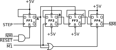
EDIT: Looking at something else I chanced upon the fact that the above circuit is nothing to do with the memory interface - it is the Nascom 2 single step circuit. I obviously overwrote the old image my error. I'll try to restore the correct diagram.

I think it should work with most 64k x 4 DRAM chips. Clock to CAS should be about 40ns with LSTTL, for a 4MHz Z80 there's a 35ns data-in set-up time so the RAM needs a CAS access time of 250-(40+35) or 175ns, give-or-take. As even the venerable 4116-25 had a TCAC of 165ns I don't foresee any problems with anything faster. For a 6Mhz system the figure will be about 100ns which shoulkd be do-able with a "150ns" DRAM.

The only thing I can see that might be iffy is whether there's enough CAS precharge time for the refresh cycle. One problem is that there is no specification for the interval between MREQ going inactive and RFSH going active - however it's probably 40 or 50ns on a 4MHz part which should be enough, 6 or 8MHz parts might become marginal here. Wiser heads might spot other mistakes I made.

If anyone does implement it, let me know if it works :)

Edit: Re-reaading the Mostek document I was reminded of one small tip which had elluded my memory - it's wise to latch any address bits which are used to generate chip select signals with the falling edge of MREQ. The Z80 doesn't guarentee that the address bus will be valid for the whole of the time that MREQ is low. Thus it is possible to get short glitches on chip select signals which can cause problems - especially when used to generate RAS signals for DRAM.
« Last Edit: August 06, 2017, 11:16:10 am by grumpydoc »
 

Offline C

  • Super Contributor
  • ***
  • Posts: 1346
  • Country: us
Re: Z80 single board memory bank switching
« Reply #48 on: August 03, 2013, 11:15:54 am »
MrAureliusR

Before you get too far you might want to take a quick look at the TurboDos Z80 Implementors Guide
As I said TurboDos lets you run CPM-80 programs while also letting Z80 machines network. TurboDos can be a standalone system like CPM-80 or be a network of Z80's.
 You should be able to find all the needed files for TurboDos online. You will just need to add the bios part which they give examples of..
The neat part is that the Z80 Implementors Guide makes this software part of bios easy to understand and create | modify. And there is enough information there that you could have a file on a pc act like a disk drive to a z80 turbodos system with a small program running on a PC.
One connection to a PC would allow console, printer & drives to be via the PC. Worth a quick look to save you time and hardware needed on the Z80 to function as a computer system.

If you would like to see the schematic of a system that pushed the limits back then, you may want to look at the Tandy Radio Shack TRS model II or TRS model 12 these are online with a description of how it works.
While not stated in the description of this system, this system has bank switched memory hardware and DMA connected IO chips. The TRS model II was also the foundation to the model 16 which is really just a add on slave card with a 68000 processor on the slave card. When running a 68K operating system on a model 16 the Z80 was the smart IO processor to the 68K leaving the 68K with more time to work on user tasks.

C


Offline netdudeuk

  • Frequent Contributor
  • **
  • Posts: 447
  • Country: gb
Re: Z80 single board memory bank switching
« Reply #49 on: November 23, 2013, 11:23:14 pm »
I've been working on a new Z80 system and I am planning on using a 74LS138 as per post #11.

I have two 8K EEPROMs which will fit nicely off the first two outputs.  I also have a 32K RAM chip which needs to sit in the top 32K of address space.  I'm thinking about using a 74LS21 (dual four input AND gate) across the 138's O4-O7 pins with the output going to the active low chip enable on the RAM chip.  The theory is that if none of the upper four 8K blocks are accessed, the output from the gate will be high, disabling the RAM chip.  The RAM chip should be enabled if any of the inputs to the LS21 goes low.

My only concern is what happens with the LS21 if the MREQ on the LS138 is high.  If the outputs from it go high impedance, could the LS21 end up in an unpredictable state ?  Would it be better to have pull-ups on the LS138/LS21 connections ?

Thanks
 

Offline grumpydoc

  • Super Contributor
  • ***
  • Posts: 2905
  • Country: gb
Re: Z80 single board memory bank switching
« Reply #50 on: November 24, 2013, 09:07:27 am »
The 74LS138 does not have tri-state outputs, inactive outputs are just at logic 1 so you don't need to worry about pull-up resistors.


Offline netdudeuk

  • Frequent Contributor
  • **
  • Posts: 447
  • Country: gb
Re: Z80 single board memory bank switching
« Reply #51 on: November 24, 2013, 09:49:51 am »
Great thanks.

« Last Edit: November 24, 2013, 09:58:36 am by netdudeuk »
 

Offline netdudeuk

  • Frequent Contributor
  • **
  • Posts: 447
  • Country: gb
Re: Simple Z80 memory interfacing pt 3
« Reply #52 on: July 09, 2017, 10:57:36 am »
OK, so the previous two examples are fine for micro-controller projects but the OP was interested in CP/M. For that you need RAM at low addresses because the TPA (i.e where programs are loaded) starts at 0x0100. Also you really need 64k of RAM if at all possible.

This all provides a bit of a problem, how do we have ROM at address 0 for the initial cold reset and RAM at address 0 when running CP/M?  I should point out BTW that for the moment I'm thinking of CP/M 2.2 and below - CP/M 3.0 supported bank switching but it wasn't around the last time I built a machine to run CP/M so I need to go and have a look at how it works.

We need to introduce some ability to switch one bank between ROM & RAM - the following (totally from memory so untested) circuit should do the trick


We now have two 32kx8 SRAM chips plus some additional gating with half a 74LS74 and a couple more OR gates. On reset the flip flop is cleared so the output will be low, this allows the chip select signal to pass to the EPROM. If a "1" is written to the flip-flop then the chip select will pass to the SRAM.

So, after a reset code in the ROM will run - as part of its initialisation it needs to copy some code up into addresses above 0x8000 and then jump to that code - the flip flop can then be switched to allow the whole 64k to be RAM.

I haven't shown how the clock input to the flip-flop is generated, so that can be considered an exercise for the reader :) but it needs to be the result of combining a decoded I/O address and the processor WR signal. I'll try to find time for some posts covering I/O interfacing in the next day or two.

Hope these posts have been helpful.

Hi

Regarding the reset for the flip flop.  Assuming that this is also connected to the processor reset pin, will the flip flop outputs always have settled before the processor is ready to read from memory for the first time ?

I guess the related question is can you also be sure that the flip flop will always have changed state fast enough for the first memory access after the bank switch request ?

I'm using a Z84C0010PEG clocked at 4MHz.

Thanks


Offline grumpydoc

  • Super Contributor
  • ***
  • Posts: 2905
  • Country: gb
Re: Simple Z80 memory interfacing pt 3
« Reply #53 on: July 11, 2017, 09:44:45 pm »
Hi

Regarding the reset for the flip flop.  Assuming that this is also connected to the processor reset pin, will the flip flop outputs always have settled before the processor is ready to read from memory for the first time ?

I guess the related question is can you also be sure that the flip flop will always have changed state fast enough for the first memory access after the bank switch request ?

I'm using a Z84C0010PEG clocked at 4MHz.

Thanks
There is plenty of time because reset going low will drive Q high (and \$ \overline{Q}\$ low). For a "normal" reset one holds \$ \overline{RESET}\$ low for at least 3 t-states which, at 750ns with a 4MHZ clock is rather longer than the propagation delay in a 74LS74. Even if one uses the "warm" reset feature (holding \$ \overline{RESET}\$ low just at the rising edge of T1 in an M1 cycle there are three clock cycles before the next read.
 

Offline netdudeuk

  • Frequent Contributor
  • **
  • Posts: 447
  • Country: gb
Re: Z80 single board memory bank switching
« Reply #54 on: July 12, 2017, 06:22:43 am »
Thanks


Share me

Digg  Facebook  SlashDot  Delicious  Technorati  Twitter  Google  Yahoo
Smf