Author Topic: EEVblog #661 - Mailbag  (Read 31326 times)

0 Members and 1 Guest are viewing this topic.

Online EEVblogTopic starter

  • Administrator
  • *****
  • Posts: 37736
  • Country: au
    • EEVblog
EEVblog #661 - Mailbag
« on: September 07, 2014, 11:50:38 pm »
Mailbag Monday
Negative Feedback T-Shirts:
NOTE: Black shirt coming shortly, bug in Teespring site...
http://teespring.com/negativefeedbackAsh
555 Timer: http://teespring.com/555timer-grey3
Warranty VOID: http://teespring.com/warrantyvoid2


Spoliers & Links:
Programmable Constant Current Dummy Load: http://www.instructables.com/id/Arduino-Programmable-Constant-Current-Power-Resist/
Conrad Retro Radio Kits:
http://www.conrad.com/ce/en/overview/2420100/Retro-Kits
Evoke Flow WIFi Radio OLED Display Repair
MiniDSO Pocket Oscilloscope (a.k.a Seed Studio DSO Quad)
http://minidso.com
Pi Power Raspberry Pit power adapter: https://www.tindie.com/products/nsayer/pi-power/
L293D H-Bridge Motor driver chip: http://www.ti.com/lit/ds/symlink/l293d.pdf
MOSFET: http://www.aosmd.com/pdfs/datasheet/ao3400.pdf
MCP1804 LDO: http://www.microchip.com/wwwproducts/Devices.aspx?product=MCP1804
Silicate rock used in solar cell manufacture
« Last Edit: September 08, 2014, 10:53:25 pm by EEVblog »
 

Offline coppice

  • Super Contributor
  • ***
  • Posts: 8642
  • Country: gb
Re: EEVblog #661 - Mailbag
« Reply #1 on: September 08, 2014, 01:20:32 am »
While the dummy load PCB is really excellent for someone's first attempt, you really couldn't see issues? The ground flood is very poor. With the shifting of just a few tracks the ground plane would have flowed between groups of traces, and the ground plane would have been much quieter. In particular, the traces under the big chip have ruined its ground plane.

Don't get me wrong. Hardly anyone does a job as good as this on their first try, but I wouldn't expect good results in EMI/ESD tests without ground plane improvements.
 

Online EEVblogTopic starter

  • Administrator
  • *****
  • Posts: 37736
  • Country: au
    • EEVblog
Re: EEVblog #661 - Mailbag
« Reply #2 on: September 08, 2014, 01:53:15 am »
While the dummy load PCB is really excellent for someone's first attempt, you really couldn't see issues? The ground flood is very poor.

Unless you flooded the top as well and then via stitched, there isn't a huge amount of improvement to be had there.
Yes, I should have mentioned that.
But it's more than good enough for a dummy load.
 

Offline Dave

  • Super Contributor
  • ***
  • Posts: 1352
  • Country: si
  • I like to measure things.
Re: EEVblog #661 - Mailbag
« Reply #3 on: September 08, 2014, 02:02:15 am »
That PiPower board could use some thicker traces. It's not like there were space limitations there. :-//
<fellbuendel> it's arduino, you're not supposed to know anything about what you're doing
<fellbuendel> if you knew, you wouldn't be using it
 

Offline coppice

  • Super Contributor
  • ***
  • Posts: 8642
  • Country: gb
Re: EEVblog #661 - Mailbag
« Reply #4 on: September 08, 2014, 02:56:03 am »
While the dummy load PCB is really excellent for someone's first attempt, you really couldn't see issues? The ground flood is very poor.

Unless you flooded the top as well and then via stitched, there isn't a huge amount of improvement to be had there.
Yes, I should have mentioned that.
But it's more than good enough for a dummy load.
My guess is the developer is a pretty smart person who has yet to realise the full benefit of continuity in the ground plane. Its easy to see how a few tracks could be moved, which would allow some of those isolated ground areas to join up. Improving the area under the MCU would take more effort. Via stitching is really a last resort you have to use when you can't achieve continuity in a single plane. It takes a lot of vias to stitch the plane together as well as a pretty narrow in-plane trace would.
 

Offline calexanian

  • Super Contributor
  • ***
  • Posts: 1881
  • Country: us
    • Alex-Tronix
Re: EEVblog #661 - Mailbag
« Reply #5 on: September 08, 2014, 04:00:30 am »
I would do a forum give away with the extra DSO, or.... Start collecting an entire set!

Charles Alexanian
Alex-Tronix Control Systems
 

Online EEVblogTopic starter

  • Administrator
  • *****
  • Posts: 37736
  • Country: au
    • EEVblog
Re: EEVblog #661 - Mailbag
« Reply #6 on: September 08, 2014, 04:01:25 am »
My guess is the developer is a pretty smart person who has yet to realise the full benefit of continuity in the ground plane. Its easy to see how a few tracks could be moved, which would allow some of those isolated ground areas to join up.

Sure, but it's still a double sided board, so you will never get a good continuous ground plane.
You can fuss around moving traces to get some extra flow and shorten power loop area, but like I said there isn't really a huge amount of improvement to be had here.
Although I haven't looked over every detail of the layout, the only thing that stands out at first glance in that area is one spot under the micro.
 

Online EEVblogTopic starter

  • Administrator
  • *****
  • Posts: 37736
  • Country: au
    • EEVblog
Re: EEVblog #661 - Mailbag
« Reply #7 on: September 08, 2014, 04:01:59 am »
I would do a forum give away with the extra DSO

Yep, should do!
 

Offline chickenHeadKnob

  • Super Contributor
  • ***
  • Posts: 1055
  • Country: ca
Re: EEVblog #661 - Mailbag
« Reply #8 on: September 08, 2014, 04:19:56 am »
 A minor nag on the power load PCB. When you have a parallel ganged  array of resisters you should input and output at diagonally opposite corners to equalize resistance/path length. like so:

        high side >---------------------------------------------------------
     res.->               I     I     I     I      ......              I     I     I     I
                             ---------------------------------------------------------->   low side

 The connector was routed to the middle of the array on one side. Those resistors will get hotter.


Online EEVblogTopic starter

  • Administrator
  • *****
  • Posts: 37736
  • Country: au
    • EEVblog
Re: EEVblog #661 - Mailbag
« Reply #9 on: September 08, 2014, 04:21:41 am »
The connector was routed to the middle of the array on one side. Those resistors will get hotter.

I haven't done the calcs, but at 1ohm a pop, I doubt it matters.


Offline Rasz

  • Super Contributor
  • ***
  • Posts: 2616
  • Country: 00
    • My random blog.
Re: EEVblog #661 - Mailbag
« Reply #11 on: September 08, 2014, 06:54:04 am »
I would do a forum give away with the extra DSO

good idea, its a shitty scope for someone with a 100MHz box on the bench, but great tool for a beginner.

edit: unless it was send because it is broken :)

edit2: DSO nano/203 could really use an addon with a panel of physical knobs and buttons. This would elevate it from shitty toy for a beginner to useful status immediately. Or an app displaying virtual buttons/knobs on a 7/10' android tablet.
« Last Edit: September 08, 2014, 06:59:42 am by Rasz »
Who logs in to gdm? Not I, said the duck.
My fireplace is on fire, but in all the wrong places.
 

Offline vk3yedotcom

  • Frequent Contributor
  • **
  • Posts: 612
  • Country: au
    • vk3ye dot com (radio articles and projects)
Re: EEVblog #661 - Mailbag
« Reply #12 on: September 08, 2014, 10:05:06 am »
A bit more about the Franzis radio kit is at

It seems to drive a speaker with a 1.5v battery - but at low volume.

Wouldn't be surprised if it's based on the MK484 or similar 1 chip TRF receiver, with a transistor or two for audio amplification.

If the above is correct Jaycar sell those chips and they make a fun project. 

If Sagan does build it I can guarantee, that unlike that digital radio, it will switch on instantly!
« Last Edit: September 08, 2014, 10:54:36 am by vk3yedotcom »
NEW! Ham Radio Get Started: Your success in amateur radio. One of 8 ebooks available on amateur radio topics. Details at  https://books.vk3ye.com
 

Offline rs20

  • Super Contributor
  • ***
  • Posts: 2318
  • Country: au
Re: EEVblog #661 - Mailbag
« Reply #13 on: September 08, 2014, 10:37:54 am »
Dave, I'm fairly sure you got sent on a tangent by a spelling mistake in the Norway letter -- what you have there is most likely a lump of refined silicon -- pure, solid silica (silicon dioxide) is transparent, also known as fused quartz, and is what the windows of the space shuttles are made of. When mixed with other things to bring the melting point down to a easily manageable level, you have standard window glass. Pure silica is definitely not shiny and metallic.

No, I think what you have there is silicon that's gone through the zone refining process. I'm jealous! All you have to do is sputter on some boron and phosphorus and demonstrate making your own transistor -- Fundamentals Friday demonstration?  :P :P

PS/ Let's not forget people who (inconsequentially, to be fair) confuse silicon with silicone...
« Last Edit: September 08, 2014, 01:45:17 pm by rs20 »
 

Offline dean1066

  • Newbie
  • Posts: 2
Re: EEVblog #661 - Mailbag
« Reply #14 on: September 08, 2014, 12:22:54 pm »
Hello,

RTFM indeed!.  The product user guide for the Evoke Flow can be downloaded from here..

http://support.pure.com/au/files.php?s=96235459dedc6db91f07f2815c3e65b7&id=4

You will be able to listen to the Amp-Hour podcast, it is listed in the Pure Connect database.

Cheers
 

Offline GreyWoolfe

  • Supporter
  • ****
  • Posts: 3651
  • Country: us
  • NW0LF
Re: EEVblog #661 - Mailbag
« Reply #15 on: September 08, 2014, 12:45:31 pm »
Dave, thanks for the extended version of the mailbag.  Fifty minutes of package opening (with the Sicilian toothpick) and discovery goodness.  Beauty! :-+ :-+
"Heaven has been described as the place that once you get there all the dogs you ever loved run up to greet you."
 

Offline rob77

  • Super Contributor
  • ***
  • Posts: 2085
  • Country: sk
Re: EEVblog #661 - Mailbag
« Reply #16 on: September 08, 2014, 01:42:45 pm »
Dave, I'm fairly sure you got sent on a tangent by a spelling mistake in the Norway letter -- what you have there is most likely a lump of refined silicon -- pure, solid silica (silicon dioxide) is transparent, also known as fused quartz, and is what the windows of the space shuttles are made of. When mixed with other things to bring the melting point down to a easily manageable level, you have standard window glass. Pure silica is definitely not shiny and metallic.

No, I think what you have there is silicon that's gone through the zone refining process. I'm jealous! All you have to do is sputter on some boron and phosphorus and demonstrate making your own transistor -- Fundamentals Friday demonstration?  :P :P

+1

definitely a pure metallic silicon ;) most probably not refined to eleven nines for growing wafer grade mono-crystal , but it's definitely metallic silicon.
 

Offline tecman

  • Frequent Contributor
  • **
  • Posts: 444
  • Country: us
Re: EEVblog #661 - Mailbag
« Reply #17 on: September 08, 2014, 01:45:20 pm »
The piece of silicon you have looks like a sawed then broken piece of a crystal used for wafers, not a mineral rock.  The surfaces are sawed (by appearance).  A standard wafer would be sawed much thinner.  The shiny appearance of the sides are the look of single crystal silicon.

paul
 

Offline Kjetil

  • Regular Contributor
  • *
  • Posts: 64
  • Country: no
Re: EEVblog #661 - Mailbag
« Reply #18 on: September 08, 2014, 02:35:48 pm »
what you have there is most likely a lump of refined silicon
Yeah, just my bad for not checking the English name for it properly, here we use Silisium for the stuff, while we use silikon for breast implants etc.. hence the confusion on my end.

I'm jealous! All you have to do is sputter on some boron and phosphorus and demonstrate making your own transistor -- Fundamentals Friday demonstration?
I got more of the stuff  ;) But I was hoping that Dave would do something like that.


The piece of silicon you have looks like a sawed then broken piece of a crystal used for wafers, not a mineral rock.  The surfaces are sawed (by appearance).  A standard wafer would be sawed much thinner.  The shiny appearance of the sides are the look of single crystal silicon.

The piece was from a large slab of silicon that measured approx 10x10x30cm (or thereabouts), and got cut by a diamond saw into very thin wafers, which was then sent somewhere in Asia for further processing. These then ended up as the cells you see in your regular solar panels. This part is the bottom, hence the "rough" surface on one side, and also has the worst quality in the batch. If I remember right the top side was >99.9% Si and the bottom was >98% Si, so you would get varying grades of wafers throughout the slab.


The letter was meant for next weeks mailbag (episode 666), forgot to write that on the front  :(
« Last Edit: September 08, 2014, 02:38:39 pm by Kjetil »
Scout leader and HAM radio operator
 

Offline G7PSK

  • Super Contributor
  • ***
  • Posts: 3861
  • Country: gb
  • It is hot until proved not.
Re: EEVblog #661 - Mailbag
« Reply #19 on: September 08, 2014, 03:53:45 pm »
Norway is or used to be one of the major producers of metallic silicon, (plenty of hydro electric) its made by reducing sand or other silicon oxides using the carbothermic  process using carbon electrodes to heat the sand to 1800 deg C or above the carbon electrodes are consumed to produce CO2 and silicon. So your silicon chips have quite a carbon footprint before they are even made.
 

Offline selkathguy

  • Supporter
  • ****
  • Posts: 88
  • Country: us
Re: EEVblog #661 - Mailbag
« Reply #20 on: September 08, 2014, 04:04:49 pm »
I'll throw in my two cents that I prefer the close-up format with you behind the camera, at least for the smaller items.  You seem to be changing around the camera to get the close-ups anyway.   I can see using the able for larger items like quadcopter kits or whathaveyou.
 
Not complaining, I'll watch either way just throwing in my vote.
 

Offline SeanB

  • Super Contributor
  • ***
  • Posts: 16281
  • Country: za
Re: EEVblog #661 - Mailbag
« Reply #21 on: September 08, 2014, 04:32:18 pm »
I had some metallurgical grade silicon from Iscor, used in steel making to improve the final material properties, and it is very different, having lots of blow holes and porosity in it. Electronics grade can be zone refined from that, and that wafer could probably be used as a transistor directly just by using a pair of needles to make point contacts on the surface and use the substrate as base.

The photoamplifier looks like it has a jfet input and a 2 transistor amplifier amplifier as well inside the can. I do have a few old data books with the actual drawings of a lot of transistor dies on it.
« Last Edit: September 08, 2014, 04:34:22 pm by SeanB »
 

Offline PSR B1257

  • Frequent Contributor
  • **
  • Posts: 330
  • Country: de
Re: EEVblog #661 - Mailbag
« Reply #22 on: September 08, 2014, 05:30:05 pm »
Hy Dave,
you missed the second line of the note of the radio-kit. It says (translatet 1:1) "For children under 14 years NOT suited".
I'm afraid Sagan has to wait a little while for this kit (it's accualy a multi-band radio, as it says on the maual) to assemble  8)

In theory, there is no difference between theory and practice. But, in practice, there is.
 

Offline wilhe_jo

  • Regular Contributor
  • *
  • Posts: 175
  • Country: at
Re: EEVblog #661 - Mailbag
« Reply #23 on: September 08, 2014, 05:48:52 pm »
Little issue with that little DC-Load.... please DO NOT USE IT WHILE YOUR PC IS CONNECTED!

If there are optos or something like this - my fault, but there isn't isolation between your load and the uC it may (so thanks to murphy it will) kill your PC-Mainboard (potential risk of a ground loop!)...

73
 

Offline vindoline

  • Supporter
  • ****
  • Posts: 324
  • Country: us
Re: EEVblog #661 - Mailbag
« Reply #24 on: September 08, 2014, 06:03:01 pm »
Rs20 is absolutely right. That is a piece of pure elemental silicon (Si). It does not occur like this in nature. It has been refined (most likely from quartz or "sand" as you call it). As it came from a photovoltaic plant, it is obviously photovoltaic "grade."  Very cool.

Dave, I'm fairly sure you got sent on a tangent by a spelling mistake in the Norway letter -- what you have there is most likely a lump of refined silicon -- pure, solid silica (silicon dioxide) is transparent, also known as fused quartz, and is what the windows of the space shuttles are made of. When mixed with other things to bring the melting point down to a easily manageable level, you have standard window glass. Pure silica is definitely not shiny and metallic.

No, I think what you have there is silicon that's gone through the zone refining process. I'm jealous! All you have to do is sputter on some boron and phosphorus and demonstrate making your own transistor -- Fundamentals Friday demonstration?  :P :P

PS/ Let's not forget people who (inconsequentially, to be fair) confuse silicon with silicone...
 

Offline T3sl4co1l

  • Super Contributor
  • ***
  • Posts: 21674
  • Country: us
  • Expert, Analog Electronics, PCB Layout, EMC
    • Seven Transistor Labs
Re: EEVblog #661 - Mailbag
« Reply #25 on: September 08, 2014, 07:18:35 pm »
Some more comments on that opto device, it could be a TIA with a simple circuit, for example I built this once upon a time:


So, a 4N35 with excellent linearity and much improved speed (~1us t_r).  This uses four additional transistors, and takes advantage of the photodiode actually being in a phototransistor, so it's kind of cheating.  But the same general idea could be used with only three transistors, for somewhat poorer performance, which might be balanced against the size of the photodiode, or other requirements for that particular device.

In short, after a little more study, I wouldn't be afraid to put voltage on that sensor and see what it does.  Got any high speed light sources to test step response? ;)

Tim
Seven Transistor Labs, LLC
Electronic design, from concept to prototype.
Bringing a project to life?  Send me a message!
 

Offline eV1Te

  • Regular Contributor
  • *
  • Posts: 186
  • Country: se
  • Your trusted friend in science!
    • richardandersson.net
Re: EEVblog #661 - Mailbag
« Reply #26 on: September 08, 2014, 09:11:40 pm »
I was laughing so hard when Dave was talking about rocks and minerals while holding silicon in his hand  :) Dave gets most things right but those few times when he goes on and on with something completely wrong is just pure humor.

By the way, why do people call it metallic silicon? It is a semiconductor and is not metallic unless doped very heavily (hence not pure silicon any more), but maybe the terminology is different in different countries?


« Last Edit: September 08, 2014, 09:42:48 pm by eV1Te »
 

Offline T3sl4co1l

  • Super Contributor
  • ***
  • Posts: 21674
  • Country: us
  • Expert, Analog Electronics, PCB Layout, EMC
    • Seven Transistor Labs
Re: EEVblog #661 - Mailbag
« Reply #27 on: September 08, 2014, 09:51:08 pm »
It's shiny, and easier to say than "semimetallic" or whatever. :P

It's still true, if referring to the luster.  Galena for example is described as having a metallic or submetallic luster.

Tim
Seven Transistor Labs, LLC
Electronic design, from concept to prototype.
Bringing a project to life?  Send me a message!
 

Offline rob77

  • Super Contributor
  • ***
  • Posts: 2085
  • Country: sk
Re: EEVblog #661 - Mailbag
« Reply #28 on: September 08, 2014, 10:03:13 pm »
I was laughing so hard when Dave was talking about rocks and minerals while holding silicon in his hand  :) Dave gets most things right but those few times when he goes on and on with something completely wrong is just pure humor.

By the way, why do people call it metallic silicon? It is a semiconductor and is not metallic unless doped very heavily (hence not pure silicon any more), but maybe the terminology is different in different countries?

i was not laughing - i rather rushed to the forum to tell him it's silicon and not the ore ;) i never laugh at someone who is wrong - it can (and actually does) happen to all of us ;)
and actually Dave knows very well how a silicon wafer looks like - he made a very nice video showing a lot of silicon IC manufacturing stuff.  and let's be realistic - the highly polished wafers with the epitaxial layer of silicon are looking way different (color, surface) than the roughly cut silicon - so no wonder if someone makes a wrong assumption (supported by incorrect wording in a letter).

and why metallic ? probably because it looks like metal and most probably because silicon is a metalloid by definition ;)
 

Offline eV1Te

  • Regular Contributor
  • *
  • Posts: 186
  • Country: se
  • Your trusted friend in science!
    • richardandersson.net
Re: EEVblog #661 - Mailbag
« Reply #29 on: September 08, 2014, 10:34:02 pm »
i was not laughing - i rather rushed to the forum to tell him it's silicon and not the ore ;) i never laugh at someone who is wrong - it can (and actually does) happen to all of us ;)
and actually Dave knows very well how a silicon wafer looks like - he made a very nice video showing a lot of silicon IC manufacturing stuff.  and let's be realistic - the highly polished wafers with the epitaxial layer of silicon are looking way different (color, surface) than the roughly cut silicon - so no wonder if someone makes a wrong assumption (supported by incorrect wording in a letter).

and why metallic ? probably because it looks like metal and most probably because silicon is a metalloid by definition ;)

I agree that it is bad to laugh at someones mistakes, but it I was not laughing to the fact that he was wrong, but to the suspense when he continued, and took the time to look up how silica was made into silicon, how it would be different from sand and if silica was mined in Norway.  :) Dave is great, I do not blame him, he should be honored that even his mistakes are amusing and attracts viewers!
 
I work as a researcher within material science and just because of my personal interest in the subject, I had to look up the properties of silicon. Interestingly it does not have a metallic luster/reflections, it behaves as a dielectric material with very high absorption.

For example metals does not polarize light when reflected of its surface, but glass/plastic and silicon does. Light can not penetrate metals, it is reflected if its top surface, but in silicon it can penetrate into the material (used in solar panels) and if thin enough it can go through, similarly to that of a highly colored glass object.

Wikipedia:
There is no standard definition of a metalloid, nor is there complete agreement as to which elements are appropriately classified as such.

« Last Edit: September 08, 2014, 10:36:41 pm by eV1Te »
 

Offline wigman27

  • Regular Contributor
  • *
  • Posts: 143
  • Country: au
    • Wiggins Wonderful Websites
Re: EEVblog #661 - Mailbag
« Reply #30 on: September 08, 2014, 10:41:25 pm »
Hi all!

A big thanks to Dave for putting my PCB on the mailbag! I'm really happy you like it!

Thanks very much for the feedback from everyone here and a big thanks again to everyone who has helped me!

This certainly is my second ever PCB and I had made a few improvements from rev A and everything works quite well! One thing I would improve in the next one is the opamp, not too happy with the offset of the LM324 but apart from that I'm pretty happy!

Thanks for the comments on my ground plane, I can certainly see what you're talking about and will definatley try and improve that in my future designs!

I think Dave must of accidentally forgot to include the links in the description of the video so here they are

http://www.instructables.com/id/Arduino-Programmable-Constant-Current-Power-Resist

www.youtube.com/playlist?list=PLzlqY1PgCfF6wMwhryeSO72kd-sh6Fgyo

https://github.com/wigman27/Arduino-Programmable-Constant-Current-Power-Resistance-Load

https://www.eevblog.com/forum/oshw/arduino-programmable-constant-current-power-resistance-load/

I'm nearly out of spare boards but if there is enough interest I will re-run it. The gerbers are also on my GitHub.

Thanks again Dave! Love the blog as always!

« Last Edit: September 09, 2014, 12:25:13 am by wigman27 »
Need a website designed? Check out my Australian based web development business www.wigweb.com.au for affordable fixed price packages
 

Offline nsayer

  • Regular Contributor
  • *
  • Posts: 133
  • Country: us
    • Geppetto Elecronics
Re: EEVblog #661 - Mailbag
« Reply #31 on: September 08, 2014, 10:53:25 pm »
That PiPower board could use some thicker traces. It's not like there were space limitations there. :-//

I could be wrong, but I thought 25 mil for the main current path was sufficient. The traces are fairly short. I wanted to insure good coverage of the groundplane as well. I even put a couple extra vias to make the ground path closer (since the groundplane on the bottom is much less interrupted) for the diode anode, input and output filter cap junctions.
Buy my stuff!! It's not at all terrible!! http://tindie.geppettoelectronics.com/
 

Offline miguelvp

  • Super Contributor
  • ***
  • Posts: 5550
  • Country: us
Re: EEVblog #661 - Mailbag
« Reply #32 on: September 08, 2014, 11:32:30 pm »
The raw pure silicon that the Avogadro project uses cost 1 million Euros, after making the perfect sphere for the new reference kilogram, it probably cost around 3 million dollars according to popular science.
 

Offline Dave

  • Super Contributor
  • ***
  • Posts: 1352
  • Country: si
  • I like to measure things.
Re: EEVblog #661 - Mailbag
« Reply #33 on: September 09, 2014, 12:02:24 am »
I could be wrong, but I thought 25 mil for the main current path was sufficient. The traces are fairly short. I wanted to insure good coverage of the groundplane as well. I even put a couple extra vias to make the ground path closer (since the groundplane on the bottom is much less interrupted) for the diode anode, input and output filter cap junctions.
AFAIK you normally give it as much copper as you can. Check out your chip's datasheet and look at the example PCB layout (page 16). There are huge copper polygons there.
<fellbuendel> it's arduino, you're not supposed to know anything about what you're doing
<fellbuendel> if you knew, you wouldn't be using it
 

Offline FrankBuss

  • Supporter
  • ****
  • Posts: 2365
  • Country: de
    • Frank Buss
Re: EEVblog #661 - Mailbag
« Reply #34 on: September 09, 2014, 01:05:16 am »
I would do a forum give away with the extra DSO

good idea, its a shitty scope for someone with a 100MHz box on the bench, but great tool for a beginner.
Is it this scope?

http://www.seeedstudio.com/depot/DSO-Nano-v3-p-1358.html?cPath=63_65

200 kHz analog bandwidth and 1 Msps is really just a toy for beginners. If you have a PC and don't need a display, this looks very good:

http://parts.arrow.com/item/detail/arrow-development-tools/bescopebundle

50 MHz analog bandwidth, 250 Msps and (kind of) a FPGA development kit integrated, for $50. Even with $38 shipping cost to Germany it is a great deal.
So Long, and Thanks for All the Fish
Electronics, hiking, retro-computing, electronic music etc.: https://www.youtube.com/c/FrankBussProgrammer
 

Offline miguelvp

  • Super Contributor
  • ***
  • Posts: 5550
  • Country: us
Re: EEVblog #661 - Mailbag
« Reply #35 on: September 09, 2014, 01:30:36 am »
Damn, I already have a BeMicro CV but I guess I have to get this as well, curse you!!!!
The BeMicro CV by itself cost me $50 a back in May.
 

Offline nsayer

  • Regular Contributor
  • *
  • Posts: 133
  • Country: us
    • Geppetto Elecronics
Re: EEVblog #661 - Mailbag
« Reply #36 on: September 09, 2014, 01:32:04 am »
I could be wrong, but I thought 25 mil for the main current path was sufficient. The traces are fairly short. I wanted to insure good coverage of the groundplane as well. I even put a couple extra vias to make the ground path closer (since the groundplane on the bottom is much less interrupted) for the diode anode, input and output filter cap junctions.
AFAIK you normally give it as much copper as you can. Check out your chip's datasheet and look at the example PCB layout (page 16). There are huge copper polygons there.

Well, Si non confectus, non reficiat.
Buy my stuff!! It's not at all terrible!! http://tindie.geppettoelectronics.com/
 

Offline miguelvp

  • Super Contributor
  • ***
  • Posts: 5550
  • Country: us
Re: EEVblog #661 - Mailbag
« Reply #37 on: September 09, 2014, 01:48:38 am »
Damn, I already have a BeMicro CV but I guess I have to get this as well, curse you!!!!
The BeMicro CV by itself cost me $50 a back in May.

For what is worth, shipping and taxes where $12.25 to the states, so $38 doesn't sound like much.
And of course Thank You instead of cursing you ;)

Other things to know about the BeMicro CV FPGA dev kit is that if you can find it (actually I did) you can get the BeUSB 3.0 evaluation board with the EZ-USB FX3 superspeed 3.0 device controller for $99 that attaches to to the custom connector of the BeMicro CV or the original BeMicro.
https://parts.arrow.com/item/detail/arrow-development-tools/beusb3.0

A bit pricey for me since I'm not doing anything with USB 3.0 anyways.

Also you can buy the InterPoser (adapter that allows you to connect Analog Devices dev boards to the BeMicro) for $50 more.

http://components.arrow.com/part/detail/NEG50150698S8959040N1911

More details here
http://www.arrownac.com/solutions/adi_interposer/

Edit: click on ADI Evaluation Boards to see what boards are available (all kinds of DAC, ADC, DDS, PLL, Wave Generators, etc.. goodness), also you'll find reference designs and the links to purchase it all of course

http://wiki.analog.com/resources/alliances/altera
« Last Edit: September 09, 2014, 02:37:17 am by miguelvp »
 

Offline FrankBuss

  • Supporter
  • ****
  • Posts: 2365
  • Country: de
    • Frank Buss
Re: EEVblog #661 - Mailbag
« Reply #38 on: September 09, 2014, 01:57:08 am »
Yeah, sometimes marketing creates interesting prices :) I found it because I got an ad eMail, promoting this: http://parts.arrow.com/item/detail/arrow-development-tools/bescope First I thought $45 is a nice price for such a scope, but then I read in the fine prints of the datasheet, that you need the BeMicro CV, too. And no link from this page to the bundle page of course. Luckily I found it with some Google searching. Looks like the usual in big companies, the right hand doesn't know what the left hand is doing.
So Long, and Thanks for All the Fish
Electronics, hiking, retro-computing, electronic music etc.: https://www.youtube.com/c/FrankBussProgrammer
 

Offline miguelvp

  • Super Contributor
  • ***
  • Posts: 5550
  • Country: us
Re: EEVblog #661 - Mailbag
« Reply #39 on: September 09, 2014, 02:10:53 am »
That interposer connector is really expensive for being just a connector, but  boy does it open a lot of analog devices possibilities!

Not sure about the 6GHz and around that frequency boards I would think the FPGA couldn't cope with that but maybe.
 

Offline hikariuk

  • Supporter
  • ****
  • Posts: 206
  • Country: gb
Re: EEVblog #661 - Mailbag
« Reply #40 on: September 09, 2014, 03:35:09 am »
The thingamabob is a Sith insignia.
I write software.  I'd far rather be doing something else.
 

Offline RupertGo

  • Regular Contributor
  • *
  • Posts: 77
Re: EEVblog #661 - Mailbag
« Reply #41 on: September 09, 2014, 06:40:12 am »
I have to rant about that Pure Evoke Flow wireless... I mean, by all that is unholy and misbegotten, look at that bloody interface! Scroll bars! Incomprehensible menu items! Lag and asynchronous messages and god knows what else hidden away in there!

And did I mention the SCROLL BARS! This is 2014! I'd be ashamed to have produced something that crapulous in 1984.

There is zero or less excuse for this sort of thing these days. Look at the sort of standard one-man-and-his-dachshund outfits are producing for free smartphone apps, while Pure are shoving this sort of manure out. No wonder DAB is dying the death of a dingo in a liquidiser with this sort of teenage Science Fair bollockry being flogged to the confused masses.

RTFM? I have hundreds of apps on my mobile, which is itself a brain-blowingly complex and capable info-tool, and I haven't had to RTFM (even if there was an FM) for any of this. And you sbould have to for a bloody radio? As that little analogue kit shows - you turn one knob to get the noise, and another to choose which noise you want. Posh version - add a band switch.  Not this crackling heap of robo-vom.

Jeez.


Offline Rasz

  • Super Contributor
  • ***
  • Posts: 2616
  • Country: 00
    • My random blog.
Re: EEVblog #661 - Mailbag
« Reply #42 on: September 09, 2014, 06:44:02 am »
good idea, its a shitty scope for someone with a 100MHz box on the bench, but great tool for a beginner.
Is it this scope?

http://www.seeedstudio.com/depot/DSO-Nano-v3-p-1358.html?cPath=63_65

200 kHz analog bandwidth and 1 Msps is really just a toy for beginners.

no, its 203/dso quad
50MHz or something analog bw
Who logs in to gdm? Not I, said the duck.
My fireplace is on fire, but in all the wrong places.
 

Offline rs20

  • Super Contributor
  • ***
  • Posts: 2318
  • Country: au
Re: EEVblog #661 - Mailbag
« Reply #43 on: September 09, 2014, 06:45:54 am »
I have to rant about that Pure Evoke Flow wireless... I mean, by all that is unholy and misbegotten, look at that bloody interface! Scroll bars! Incomprehensible menu items! Lag and asynchronous messages and god knows what else hidden away in there!

And did I mention the SCROLL BARS! This is 2014! I'd be ashamed to have produced something that crapulous in 1984.

There is zero or less excuse for this sort of thing these days. Look at the sort of standard one-man-and-his-dachshund outfits are producing for free smartphone apps, while Pure are shoving this sort of manure out. No wonder DAB is dying the death of a dingo in a liquidiser with this sort of teenage Science Fair bollockry being flogged to the confused masses.

RTFM? I have hundreds of apps on my mobile, which is itself a brain-blowingly complex and capable info-tool, and I haven't had to RTFM (even if there was an FM) for any of this. And you sbould have to for a bloody radio? As that little analogue kit shows - you turn one knob to get the noise, and another to choose which noise you want. Posh version - add a band switch.  Not this crackling heap of robo-vom.

Jeez.

Except your phone has a powerful CPU and GPU that makes even face-palmingly poorly written routines run seemingly instantaneously, multiple cores, millions of colour pixels, a OS and software development kit with all the GUI and threading groundwork done for you, and a touch screen. I agree that the interface was on the radio was poor, but saying that the average person who can make a useable app could do a better job here is just completely ridiculous.
 

Offline Rasz

  • Super Contributor
  • ***
  • Posts: 2616
  • Country: 00
    • My random blog.
Re: EEVblog #661 - Mailbag
« Reply #44 on: September 09, 2014, 06:54:45 am »
I have to rant about that Pure Evoke Flow wireless... I mean, by all that is unholy and misbegotten, look at that bloody interface! Scroll bars! Incomprehensible menu items! Lag and asynchronous messages and god knows what else hidden away in there!

And did I mention the SCROLL BARS! This is 2014! I'd be ashamed to have produced something that crapulous in 1984.

There is zero or less excuse for this sort of thing these days. Look at the sort of standard one-man-and-his-dachshund outfits are producing for free smartphone apps, while Pure are shoving this sort of manure out. No wonder DAB is dying the death of a dingo in a liquidiser with this sort of teenage Science Fair bollockry being flogged to the confused masses.

RTFM? I have hundreds of apps on my mobile, which is itself a brain-blowingly complex and capable info-tool, and I haven't had to RTFM (even if there was an FM) for any of this. And you sbould have to for a bloody radio? As that little analogue kit shows - you turn one knob to get the noise, and another to choose which noise you want. Posh version - add a band switch.  Not this crackling heap of robo-vom.

Jeez.

Except your phone has a powerful CPU and GPU that makes even face-palmingly poorly written routines run seemingly instantaneously, multiple cores, millions of colour pixels, a OS and software development kit with all the GUI and threading groundwork done for you, and a touch screen.

all than and phone is still CHEAPER
if you really want networked radio get cheap chinese tablet, or second hand android phone, not this piece of crap evoke whatever
Who logs in to gdm? Not I, said the duck.
My fireplace is on fire, but in all the wrong places.
 

Offline Paul Moir

  • Frequent Contributor
  • **
  • Posts: 926
  • Country: ca
Re: EEVblog #661 - Mailbag
« Reply #45 on: September 09, 2014, 07:17:00 am »


no, its 203/dso quad
50MHz or something analog bw

Unfortunately not even close to this.  They botched the analog frontend leading to a huge dip between about 1MHz and something like 7.  Some hacked it to get a pretty good rolloff -3db@10MHz.  But still it's fundamentally flawed in a few ways.

Really it was a huge disappointment.  One wonders what could have happened if they had involved the community at the design stage.

Gory details:
http://www.seeedstudio.com/forum/viewtopic.php?f=26&t=1944
 

Offline RupertGo

  • Regular Contributor
  • *
  • Posts: 77
Re: EEVblog #661 - Mailbag
« Reply #46 on: September 09, 2014, 07:18:45 am »
Who says you have to use a slow CPU and a dumb display? These are being presented and sold, often, as premium products: I know there's not the same economy of scale as with smartphones, but the disparity is far too wide to make any sense.

If there's no economic way to make a digital radio with a decent interface, then there's no economic way to make a digital radio.
 

Offline rs20

  • Super Contributor
  • ***
  • Posts: 2318
  • Country: au
Re: EEVblog #661 - Mailbag
« Reply #47 on: September 09, 2014, 07:49:40 am »
Who says you have to use a slow CPU and a dumb display? These are being presented and sold, often, as premium products: I know there's not the same economy of scale as with smartphones, but the disparity is far too wide to make any sense.

If there's no economic way to make a digital radio with a decent interface, then there's no economic way to make a digital radio.

I'm not necessarily defending the quality of the Evoke, I'm just saying that a comparison to single-man phone apps is the height of irrelevance. I'd hazard to guess that whatever hardware is in there is capable of operating in a snappy and intuitive way; it's just the software that sucks. Just like it would if a single-man app writer tried to write it.

all than and phone is still CHEAPER

Yes, economies of scale are amazing.

if you really want networked radio get cheap chinese tablet, or second hand android phone, not this piece of crap evoke whatever

Great, no AM, no FM, crap speakers, looks weird on the table-top. I agree with you, I don't want one of these either, but I can't help but feel that you're missing the point of this thing. Something to do with style or fashion or something weird like that.
 

Offline Rasz

  • Super Contributor
  • ***
  • Posts: 2616
  • Country: 00
    • My random blog.
Re: EEVblog #661 - Mailbag
« Reply #48 on: September 09, 2014, 09:51:33 am »


no, its 203/dso quad
50MHz or something analog bw

Unfortunately not even close to this.  They botched the analog frontend leading to a huge dip between about 1MHz and something like 7.  Some hacked it to get a pretty good rolloff -3db@10MHz.  But still it's fundamentally flawed in a few ways.

Really it was a huge disappointment.  One wonders what could have happened if they had involved the community at the design stage.

Gory details:
http://www.seeedstudio.com/forum/viewtopic.php?f=26&t=1944

doh, never mind then :)

another alternative might be labtool based on LPC4370 (ARM M4 with 80MHz 12bit ADC buildin)
http://www.lpcware.com/content/project/Mixed-Signal-Logic-Analyzer-Oscilloscope-Lab-Tool-Solution
http://www.embeddedartists.com/products/app/labtool.php

~$150
software is pure shit tho, as always :)

how is the software for BESCOPE?

btw Chris was looking for cheap scope for his course, BESCOPE might be it (fpga as added bonus).
« Last Edit: September 09, 2014, 09:57:20 am by Rasz »
Who logs in to gdm? Not I, said the duck.
My fireplace is on fire, but in all the wrong places.
 

Offline FrankBuss

  • Supporter
  • ****
  • Posts: 2365
  • Country: de
    • Frank Buss
Re: EEVblog #661 - Mailbag
« Reply #49 on: September 09, 2014, 10:56:38 am »
how is the software for BESCOPE?
It looks very basic, like something someone hacked with LabVIEW in some hours, see page 16 of the datasheet, but should be sufficient as a basic scope. There is a link in the datasheet where you can download the software, with the note "TBD" and of course the page doesn't exists and I can't find a download link on the shop page either. I hope when I get it that it comes with a CD with the software, but all this doesn't inspiring confidence. Well, I guess you get what you pay for. Someone should hack the PicoScope software to use it with the BeScope :)
So Long, and Thanks for All the Fish
Electronics, hiking, retro-computing, electronic music etc.: https://www.youtube.com/c/FrankBussProgrammer
 

Offline Rasz

  • Super Contributor
  • ***
  • Posts: 2616
  • Country: 00
    • My random blog.
Re: EEVblog #661 - Mailbag
« Reply #50 on: September 09, 2014, 12:50:39 pm »
JAVA backend!! this is pretty retarded
"capative tuner" in pdf doesnt look promising either
yeeep, whole fpga firmware was drag&dropped in some Altera wizard :(
software has ac/dc coupling switch, diagram shows hardwired DC coupling
whole thing was designed by nck research (two ethernet guys - thats what they say about themselves)
its rev 1
at least python UI comes with source code

AD logo on PCB at least suggests a possibility AnalogDevices had some decency and made one of their grey beards look at the design and maybe even tune the front end so its not pure shit, but im probably dreaming :) screenshot shows 2.5MHz square wave and it looks passable


found software link
http://www.arrownac.com/solutions/bescope/downloads/BeScope_Installation_package_8-7-14.zip

$50 made me want to buy it, but shipping is pretty lol, I refuse to pay $40 for shipping, F that


aaand good read here:
http://forums.parallax.com/showthread.php/157115-BeScopeBundle-System-Files

broken software, shipped not programmed, idiots responding to support mails. Sounds just as good as any chinese USB scope :D
Who logs in to gdm? Not I, said the duck.
My fireplace is on fire, but in all the wrong places.
 

Offline FrankBuss

  • Supporter
  • ****
  • Posts: 2365
  • Country: de
    • Frank Buss
Re: EEVblog #661 - Mailbag
« Reply #51 on: September 09, 2014, 02:22:44 pm »
aaand good read here:
http://forums.parallax.com/showthread.php/157115-BeScopeBundle-System-Files

broken software, shipped not programmed, idiots responding to support mails. Sounds just as good as any chinese USB scope :D
YYMD. He is probably right how the software was developed. A FTDI chip, which sends samples in ASCII to a TCL script, which sends it to a Python script, which provides a TCP/IP interface and then a Java program which displays it!? |O
So Long, and Thanks for All the Fish
Electronics, hiking, retro-computing, electronic music etc.: https://www.youtube.com/c/FrankBussProgrammer
 

Offline miguelvp

  • Super Contributor
  • ***
  • Posts: 5550
  • Country: us
Re: EEVblog #661 - Mailbag
« Reply #52 on: September 09, 2014, 02:36:11 pm »
I did order one anyways.

I guess what I'm getting from that thread is to only use the code as a reference guide and roll my own. What I'm I getting into?  :scared:
 

Offline miguelvp

  • Super Contributor
  • ***
  • Posts: 5550
  • Country: us
Re: EEVblog #661 - Mailbag
« Reply #53 on: September 10, 2014, 12:30:27 am »
By looking at what comes with the kit I noticed this,

Kit Includes for $50 the following:

BeMicro CV Eval Kit $49
SDP Interposer $50
mini USB cable $whocares
oscilloscope probe $10 (cheap 150MHz probe at best)
BeScope Daughter Card $45

Just the InterPoser goes for $50 and opens me up for the first part of these (the SDP connector ones):
http://wiki.analog.com/resources/alliances/altera

Also looking at the docs, the ADC can be configured to a single channel 500MSPS instead of the dual channel 250MSPS each.

The code is a mess but at least they do seem to have a full QSys system without NIOS, not confirmed but I will look at it later.
Also there are some free lvds (at least 4 pair channels) left and one I2C (2 pins) also not connected. The InterPoser offers extra pins not used by the other headers, for what I read in the forum is 60 more available via the InterPoser SDP connector.


Offline Rasz

  • Super Contributor
  • ***
  • Posts: 2616
  • Country: 00
    • My random blog.
Re: EEVblog #661 - Mailbag
« Reply #54 on: September 10, 2014, 06:10:04 am »
Also there are some free lvds (at least 4 pair channels) left and one I2C (2 pins) also not connected. The InterPoser offers extra pins not used by the other headers, for what I read in the forum is 60 more available via the InterPoser SDP connector.

I think someone on parallax forum said bescope pcb has all unused IO grounded
Who logs in to gdm? Not I, said the duck.
My fireplace is on fire, but in all the wrong places.
 

Offline miguelvp

  • Super Contributor
  • ***
  • Posts: 5550
  • Country: us
Re: EEVblog #661 - Mailbag
« Reply #55 on: September 10, 2014, 06:29:13 am »
The doc shows them as N/C so I hope they are not connected at all, if they are (connected to ground), well there are an extra 60 pin on the edge connector, will have to look into the FPGAs datasheet to see if they can do LVDS (the BeMicro docs don't show much detail on those other than 2.5V and 3.3V capable), otherwise I have a video 3 channel dac that I could use to drive an SVGA signal.

Edit: but since the edge connector interfaces with other analog devices dev boards they must have some lvds signals lying around.
« Last Edit: September 10, 2014, 06:43:23 am by miguelvp »
 

Offline miguelvp

  • Super Contributor
  • ***
  • Posts: 5550
  • Country: us
Re: EEVblog #661 - Mailbag
« Reply #56 on: September 15, 2014, 11:05:09 pm »
The BeScope showed up today and it's almost time to leave work and go play with it :)

Thanks to the work of the user thoth at the parallax propeller forum I should be able to get it running in no time.
Ill see how well it does with a composite signal if I'm successful at getting it running.

Then I'll see how much an ADI module from Analog devices are to make an ARB or DDS since now I have the SDP Interposer and an spare BeMicro CV.

Oh, and BeMicro is coming with a CV-A9 version with a beefier Cyclone V if it doesn't get cancelled.


Offline miguelvp

  • Super Contributor
  • ***
  • Posts: 5550
  • Country: us
Re: EEVblog #661 - Mailbag
« Reply #57 on: September 16, 2014, 03:51:51 am »
So I got it all setup and no errors anywhere but I get no test signal (measured with my rigol to make sure) and it doesn't display a thing. I did use my existing board and made sure the VCCIO jumper is set to 3.3V, so I guess the next thing is to supply the extra 5V with the microUSB connector on the ADC board.

Or maybe I'll use the supplied board but it looks like it's the same thing.

BTW I did test all the N/C pins and they are not grounded nor connected to anything. Not even the Device and Pin Options has them set as grounded, the project has the unused pins set to as input tri-stated.

The probe it came with it is a 100MHz probe, they look like the UNI-T probes I got from mortoncontrols but 100MHz instead of 300MHz.
https://www.mortoncontrols.com/index.php/clearance/utp06.html

It does feel cheaper material wise but not terrible, but they go on ebay for under $10 (model P6100)

« Last Edit: September 16, 2014, 04:53:54 am by miguelvp »
 

Offline miguelvp

  • Super Contributor
  • ***
  • Posts: 5550
  • Country: us
Re: EEVblog #661 - Mailbag
« Reply #58 on: September 16, 2014, 04:36:45 am »
What do you know, it only needed the 5V supply to the ADC board. Edit: seems like the half amp my PC can supply is not enough to power both the BeMicro and the BeScope, probably with a powered hub it might work without powering both boards.

Not much I can do with it yet because the software is very limited to adjust to longer time periods but it's a pretty good base to start with.

By the way, it gets pretty warm!

Pictures of the device generating 2.5MHz and 5.0MHz ringing square waves as well what the DS2202 sees.

2.5MHz:


5.0MHz:


Rigol:


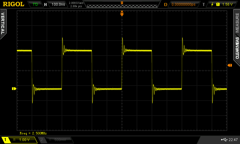
The last two attachments are the full res captures, the ones in here where resized to be 800 pixels wide instead of 1324 pixels wide.

Edit: Not bad at all for just $50, the thing I'm more exited about is the SDP Interposer so I can connect to other Analog Devices boards.

http://wiki.analog.com/resources/alliances/altera

Also the connector Analog Devices uses is a Hirose FX8-120S-SV that mates with the FX8-120P-SV in the Interposer, they are fairly cheap.

Edit: BTW the reference clock comes from an SIT8033AC-31-25A-5.00000 2-Frequency Select Oscillator in this case it's a 5MHz divisible by two with by driving the FS pin. Looks very precise (the clock not the BeScope).
http://www.sitime.com/products/datasheets/sit8033/SiT8033-datasheet.pdf

I can't find any in stock but I've seen other frequencies/dividers available.

I wonder if the output can be cleaned up, the output clock is pulled down by a 1K 1/8W 1% resistor.

« Last Edit: September 16, 2014, 08:26:13 am by miguelvp »
 

Offline tjringsmose

  • Newbie
  • Posts: 3
Re: EEVblog #661 - Mailbag
« Reply #59 on: September 16, 2014, 12:24:18 pm »
About that SMD dev board.
I know that the pin pitch array is a common technique, but I can't shake the feeling that a chip with a ground pad, is wound to short some pins, especially on the larger packages. Do you scrape off the solder pads or is it a non-issue?
 

Offline rs20

  • Super Contributor
  • ***
  • Posts: 2318
  • Country: au
Re: EEVblog #661 - Mailbag
« Reply #60 on: September 16, 2014, 01:06:52 pm »
About that SMD dev board.
I know that the pin pitch array is a common technique, but I can't shake the feeling that a chip with a ground pad, is wound to short some pins, especially on the larger packages. Do you scrape off the solder pads or is it a non-issue?

Most such packages don't have a ground pad. I think if they do have a ground pad, you want a specific adapter board, rather than a one-size-fits-all -- if only because the thermal dissipation just isn't there.
 

Offline simingx

  • Contributor
  • Posts: 41
  • Country: sg
Re: EEVblog #661 - Mailbag
« Reply #61 on: October 08, 2014, 09:02:32 am »
Oh hey, I see my package there (large Singapore Post box) :D
Nice to know it showed up after 1 month in transit (I think Dave will like it, it's a piece of retro HP gear :)

Can't wait for the unboxing/teardown/educational video  O0


Share me

Digg  Facebook  SlashDot  Delicious  Technorati  Twitter  Google  Yahoo
Smf