Solder wetting does not look very well on the other inductor, either.
Reflow temperature may be too low, or components solder contacts have quality issue.
The non broken side of the inductor also came off too easily, so bad solder wetting is very probable.
To me the wetting looks fine because the so called solder meniscus looks exactly like it should be. Here's an example of how the solder meniscus should look, and the one in the Brymen meter looks fine too for Pb-free solder. (attachment, upper joint, lower joint may have been contaminated).
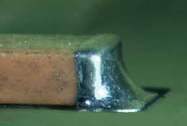
Bad solder wetting looks like this:

The case seems to be molded, so correct dry pack handling would be necessary.
If the package was left open too long, the component may have sucked in water, which cracks the case during reflow process.
In either way, high probability of two kinfd of series problem.
If that were the case, then the whole series of multimeters that was produced from the same lot of inductors would have shown problems. Assuming this happened, then this might be the first and more will follow eventually. But I doubt it and agree with Dave's asessment that this might be a one off bad inductor.
I have come across SMD components that were knocked off by carelessness. Sometimes the end caps remain in the solder, but often, and despite correct wetting, you're left with just solder. Especially SMD aluminium caps are prone to that. There's a thin intermetallic layer between the solder and the pads and the solder and the component leads. It is this layer that may be responsible for the tearing of an otherwise correct solder joint.
In this particular case, I' assuming that vibrations from transport may have broken the already weak inductor and then shaken loose the other pin as well on this intermetallic layer. Judging by the attachment, the goo from the inductor may have contaminated the solder without affecting wetting.
To me it looks to be a molding error. The goo under the inductor is probably not flux residue from the solder process. I think it's reasonable to assume that the inductor is molded from two part stuff (epoxy?) and that on this one the mixing didn't happen correctly.
Edit: looking at the attachment again, I can't help but think that the left inductor is too small to fit correctly on the pads. The end caps barely meet the pads! I think that according to the IPC610 standards, that's a no no.
Exactly, the solder meniscus SHOULD look like in your GOOD example, but to me, it does not look like that at all, actually.

The video is not so good, so I tried an enlarged view with contrast improvement, and all the right sides of the components, where the light's shining on, all look really crappy and irregular.
Especially, the right side of the other inductor looks like your BAD case photo.
Maybe, a better photo with good illumination may show different, but here, the solder did not build a meniscus at all.
You cannot ignore, how easily Dave could bend away the inductor on the left side, and if you look closely, you still can see the rectangular imprint of the component inside the solder blob.. so it really hasn't been wetted correctly.. that's the only possible explanation.

And yes indeed, that can really be a series problem @Brymen, with their reflow soldering and maybe with dry pack handling (probably not a component problem)
1/1000 is 1000ppm already, that's much too much, as undetected soldering errors (especially when using AOI) must be in the sub ppm range, nowadays.. believe me, I got a lot of experience from automotive mass production.
Frank
PS: your own photo, showing both inductors side-by-side shows even much better, how bad both are soldered, you can clearly see the lack of the meniscus, and the black spots indicate bad solder junction.. should shine completely.
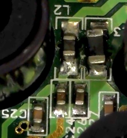
Here's a more contrasty version.. all junctions look crappy.
Maybe, that area of the PCB was in a thermal shadow, i.e. had seen lower temperatures than other parts.


