Author Topic: Use of long pads on prototyping PCBs  (Read 1257 times)

0 Members and 1 Guest are viewing this topic.

Offline petertTopic starter

  • Regular Contributor
  • *
  • Posts: 178
  • Country: de
Use of long pads on prototyping PCBs
« on: September 14, 2018, 06:01:57 pm »
Hi,

I have seen long pads at the borders of cheap PCBs you can get from amazon or ebay, but don't quite get what they are used for.

See here for example:


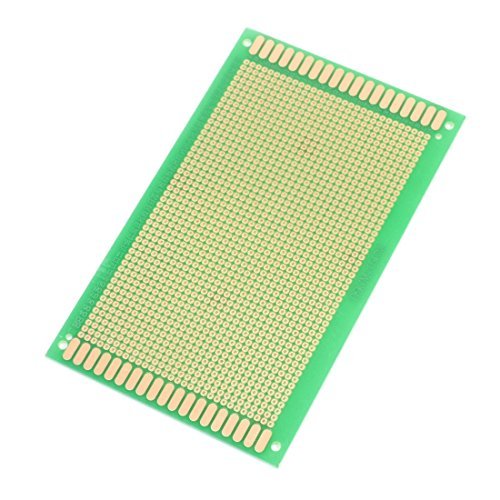
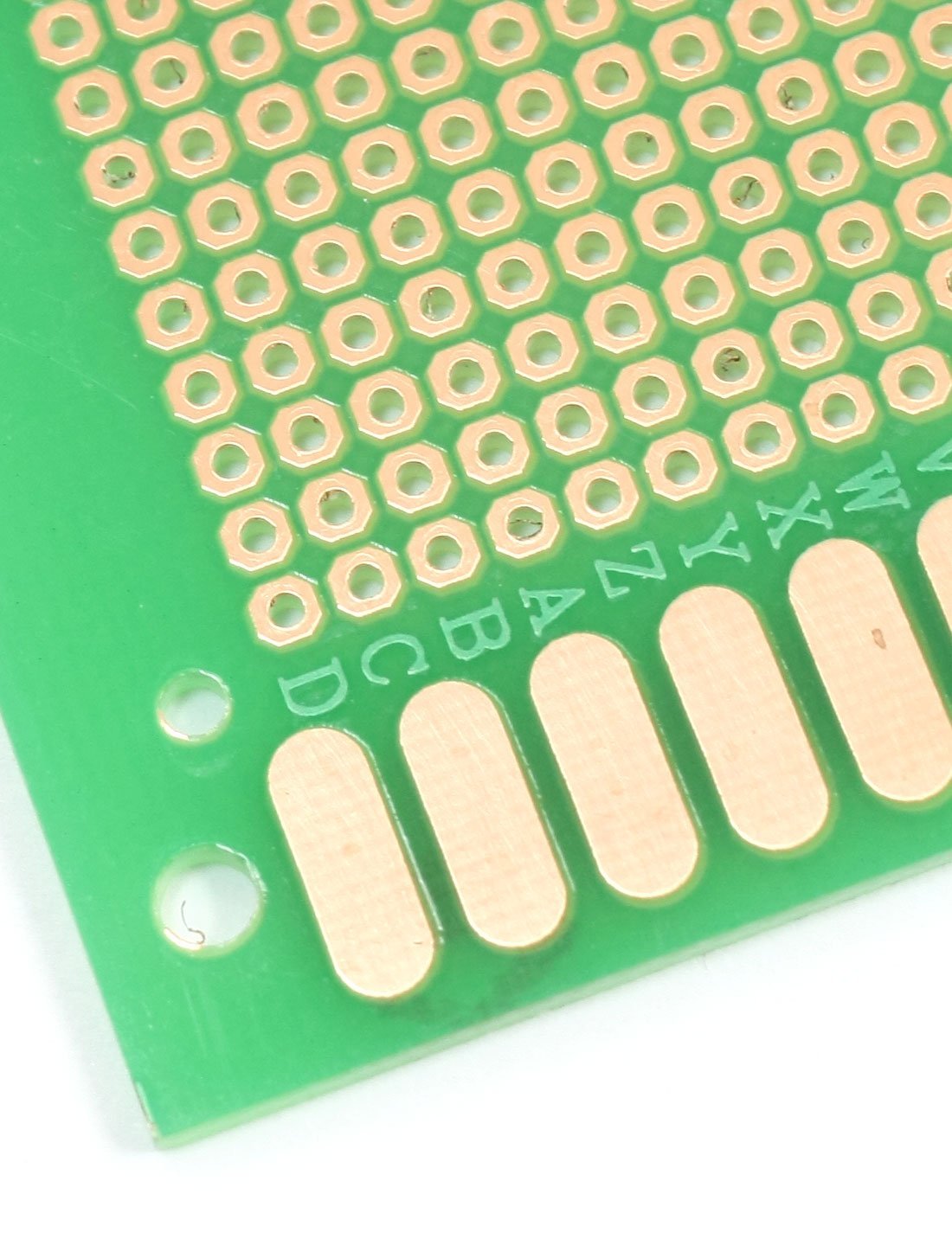
I would think they could be plugged into some kind of socket, like PCI/ISA/etc. cards, but I never found a matching socket/receptable, and they are rounded, unlike usual pads for such sockets.

What would be a "standard" use for them? And what are typical receptors/connectors for them?
« Last Edit: September 14, 2018, 06:04:39 pm by petert »
 

Offline rx8pilot

  • Super Contributor
  • ***
  • Posts: 3634
  • Country: us
  • If you want more money, be more valuable.
Re: Use of long pads on prototyping PCBs
« Reply #1 on: September 14, 2018, 06:08:24 pm »
I think they are used for wires or headers. Not sure there is a specific purpose other than providing some alternate way of soldering something to it.
Factory400 - the worlds smallest factory. https://www.youtube.com/c/Factory400
 
The following users thanked this post: petert

Offline dferyance

  • Regular Contributor
  • *
  • Posts: 181
Re: Use of long pads on prototyping PCBs
« Reply #2 on: September 14, 2018, 06:40:24 pm »
I've used them to solder flat male headers to them. You can get angled headers through-hole but then the board can be in the way.
 
The following users thanked this post: petert


Share me

Digg  Facebook  SlashDot  Delicious  Technorati  Twitter  Google  Yahoo
Smf