I'm working on a temperature control/power PCB for a TEC based water chiller. This will be used in a high end PC for CPU cooling.
The cooling system looks like this:
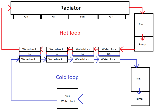
The requirements are:
1. The power input used for the TECs is 12V from a PC power supply (using PCI-E 8-pin connectors)
2. The board must be able to output 12V to the TECs at full power.
3. No electromechanical relays.
4. TEC cooling power controlled based on coolant temp, and current dew point of the ambient air.
5. Software monitoring and control of the system.
I had 3 basic options for the temperature control:
1. Thermostat-like on/off
2. PWM
3. Voltage-based
#1 is the simplest to implement, but it will cause increased thermal cycling of the TECs.
#2 is straightforward, but I'm worried about what PWM switching of a large load will do to a PC power supply.
#3 is the most complex, and I don't see a good way to get a voltage regulator with maximum voltage equal to the input voltage.
I decided to go with the PWM based design. The circuit I'm using looks like this:
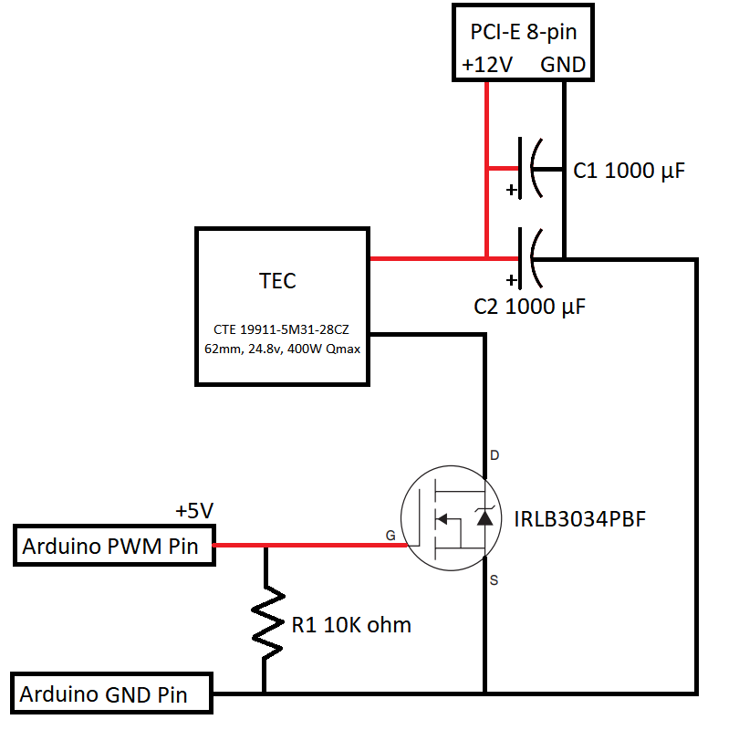
Relevant datasheets:
https://www.infineon.com/dgdl/irlb3034pbf.pdf?fileId=5546d462533600a40153566027b22585https://customthermoelectric.com/media/wysiwyg/TEC_spec_sheets/19911-5P31-28CZ_spec_sht.pdfThe 10K resistor is to pull down the MOSFET gate if the Arduino-based control device is not powered. The 2 capacitors are for decoupling. The TEC will pull roughly 12.5A when operating at 12V, or 150W. I have built a prototype of this circuit and it does appear to work correctly. The power consumption scales ~linearly with the PWM duty cycle, and the MOSFET doesn't seem to heat up much.
Circuit questions:
1. Is my choice of decoupling capacitor size sufficient? If not, how would I calculate the correct size?
2. Is there a certain PWM frequency that would be better? It must be at least 1KHz per the TEC manufacturer, but outside of that I don't know what would be best.
If there are no major flaws in the basic circuit, the next part is getting it onto a PCB. I'm new to PCB design, but I was able to create this:
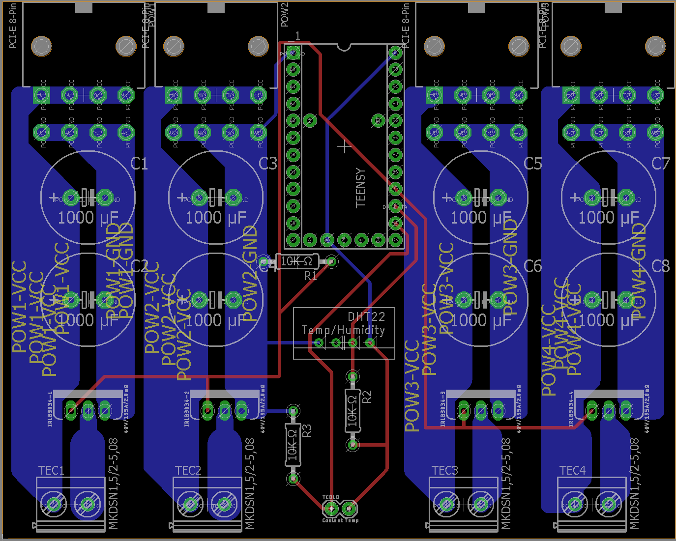
It's a 2-layer design. I'm going to use a Teensy 2.0 to control everything:
https://www.pjrc.com/store/teensy_pins.htmlThat version has header pins, which I plan to through-hole solder onto the larger power PCB. This simplifies the board because I will be able to solder all the components myself.
My main concern is the trace width for the high current nets. I used the calculator here:
http://www.4pcb.com/trace-width-calculator.htmlAccording to that, I need 96.3 mil trace width for 12.5A @ 10C rise using 4oz copper. I used 100 mil minimum trace width for them in the design above, but attempted to make them much wider where possible.
PCB questions:
1. Am I handling the high current traces correctly? If not, what do I need to change?
2. Is there anything else that appears to be wrong? This is my first PCB so I may have missed something.
Thanks for looking.


