Author Topic: Need advice for ADC Buffer  (Read 23223 times)

0 Members and 1 Guest are viewing this topic.

Offline CrossphasedTopic starter

  • Regular Contributor
  • *
  • Posts: 127
  • Country: us
Need advice for ADC Buffer
« on: December 28, 2017, 08:55:32 pm »
I'm putting together a precision voltmeter w/ a 24 bit ADC, and I'm struggling to get the buffer to the ADC  correct. The ADC used is the LTC2440, with a 5V LTC6655 reference. The assembly has been completed, but I need to re-work the ADC input buffer section. Here's a few pictures:
The ADC and the LTC6655 are covered by the gold shields


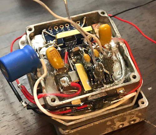
The analog and digital grounds are seperate, and the shield seperates the analog from the digital side


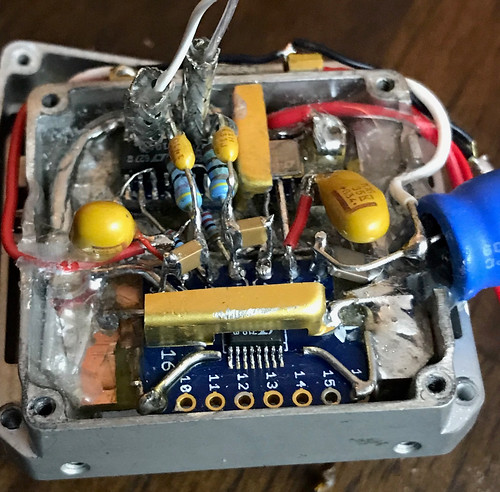
The 5V supply to the ADC is from an LT1461, and the (+) power supply to the buffers is from an LT3080. I'd like to use a single supply to the buffer amps if possible. Everything is powered from a 9V battery. The voltmeter is only used to measure positive DC voltages.

I'm having trouble with the input buffer to the ADC, specifically how to reference the differential inputs to the ground of the buffers. I'm somewhat new to op-amps. What I'm looking for is unity gain, and can handle a common mode voltage of +10-30 V. The desired output of the buffer is 0 -5 V. A little above 0 and a little less than 5 is ok and can be removed with calibration. On my first attempt I made the mistake picking opamps without taking into account how far they were able to swing compared to their power supply. So this is my second attempt. I went back to the datasheet for the 2440, and examined their buffer circuit using chopper amps:

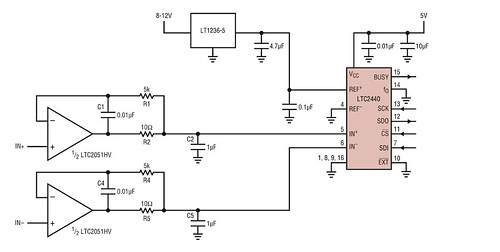
My plan is to use this circuit for the buffer, and I've got the LTC2051 here ready to use. To validate before installing, I made a test circuit using this schematic with LTC1050's, and found the output to bounce around wildly if the inputs didn't have a DC path to ground. A single supply of +6V was used for the 1050's, and a single AA battery of ~1.58 was applied to the inputs. I tried some other configurations as well, here's my results so far:

1)  Referenced both inputs to ground using 10K resistors


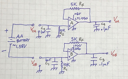
I measured the input voltages Via and Vib with reference to ground. Vib turned out to be negative and I quickly realized I had made a voltage divider with the center grounded:

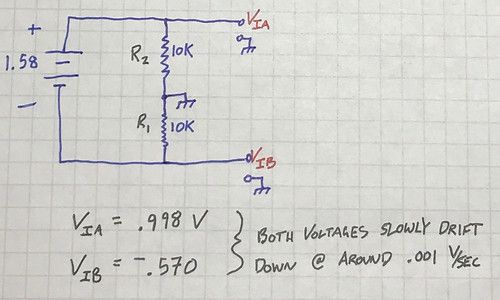
There isn't a negative supply so the output Vob was ~16 mV above ground, and Voa was ~1 V. No good.  I was somewhat surprised to see the voltage wasn't split evenly.  Maybe apply +2.5 V to the middle of R1 and R2 to correct the offset?

2)  Removed the ground connection between R1 and R2
I've read the buffers always need a DC return for the inputs, so R1 and R2 were connected to each other, essentially floating relative to the buffer grounds:

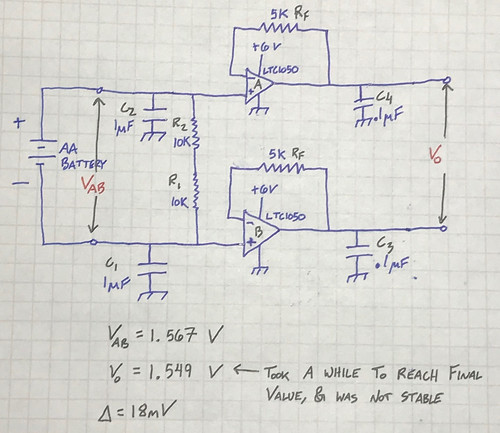
This produced better results, but it was clear the output was not very stable. It took quite some time to reach the final value, slowly rising to it. Blowing on the circuit would cause the output to jump 10-20 mV. Also, the offset of 18 mV,  is that normal?

3)  Grounded the battery to the buffer ground. This produced the best results

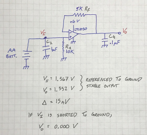
I see an offset of 15 mV again, is that a normal condition? The datasheet of the 1050 states an offset voltage of around 5 microvolts. If I'm doing something wrong here please let me know! Also if any of the passive component values are incorrect please advise. Circuit #3 produced the best results but ideally I'd like to avoid tying the V- input to ground. There is a high common mode voltage in the application, anywhere from 10-30VDC.

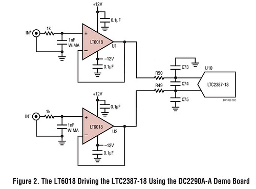
I've read through various datasheets looking for ideas, but I'm hoping someone more experienced than I can steer me in the right direction. Here's a few different buffer circuits I've found:


Looks like they get away with floating the inputs here?


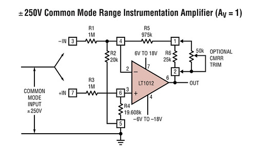
Interesting unity gain with CMRR trim


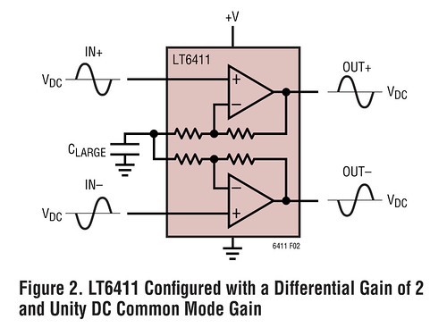
This circuit doesnt look all that different from my circuit #2, but with an added cap to ground


Any expertise you can offer would be very much appreciated! Thanks!


Offline fcb

  • Super Contributor
  • ***
  • Posts: 2117
  • Country: gb
  • Test instrument designer/G1YWC
    • Electron Plus
Re: Need advice for ADC Buffer
« Reply #1 on: December 28, 2017, 09:11:35 pm »
If you need a high-common mode voltage either:

1. Float your whole ADC block - this will give you the maximum accuracy, at the expense of complexity.
2. Use some potential dividers and measure each side of the battery, you'll through away some resolution and you'll have to watch the TC matching of the potential dividers.
3. Build a high-voltage diff amp to bring your difference down to a more ADC friendly level.

Choose your poison.
https://electron.plus Power Analysers, VI Signature Testers, Voltage References, Picoammeters, Curve Tracers.
 

Offline CrossphasedTopic starter

  • Regular Contributor
  • *
  • Posts: 127
  • Country: us
Re: Need advice for ADC Buffer
« Reply #2 on: December 28, 2017, 10:17:54 pm »
If you need a high-common mode voltage either:

1. Float your whole ADC block - this will give you the maximum accuracy, at the expense of complexity.
2. Use some potential dividers and measure each side of the battery, you'll through away some resolution and you'll have to watch the TC matching of the potential dividers.
3. Build a high-voltage diff amp to bring your difference down to a more ADC friendly level.

Choose your poison.

Thank you fcb,
How would I go about option number 1? That's the root of my question in this thread. What topology would you use to accomplish floating the ADC block?
 

Offline fcb

  • Super Contributor
  • ***
  • Posts: 2117
  • Country: gb
  • Test instrument designer/G1YWC
    • Electron Plus
Re: Need advice for ADC Buffer
« Reply #3 on: December 28, 2017, 11:30:18 pm »
You have two problems with #1.

a. isolate the digital signals between the microcontroller and your ADC - easily solved with a digital isolator, something like the Si8661/2, ISO7240 or similar. I've been quite impressed by the low-jitter of the MAX1443x range recently.

b. isolate the power to the ADC - less easily solved, solutions range from one of those $4 SIP 1W isolators (pretty noisy), building your own DC/DC with off-the-shelf magnetics through to low capacitance, high voltage isolation using my own wound transformers on coated ferrite cores.
https://electron.plus Power Analysers, VI Signature Testers, Voltage References, Picoammeters, Curve Tracers.
 

Offline danadak

  • Super Contributor
  • ***
  • Posts: 1875
  • Country: us
  • Reactor Operator SSN-583, Retired EE
Re: Need advice for ADC Buffer
« Reply #4 on: December 28, 2017, 11:40:22 pm »
Some questions -

First your LSB = 300 nV

1) What is your design goal for accuracy ? Is it absolute accuracy or relative.
2) What is the T range the accuracy spec has to operate over ?

You have to perform an end to end error analysis to see if your goals can be met.
@24 bits you will quickly find your accuracy degrades, over T, to << 16 bits, w/o
extraordinary measures. PSRR, Linearity, Offsets V and I, thermoelectric effects,
electro-chemical effects......


Here are some ap notes covering basics for many of these error topics -


https://www.dropbox.com/s/plck7e95v7pw33c/CMR%20Analysis%20IA.pdf?dl=0


https://www.dropbox.com/s/aq8pyz7d9oc8r5t/analog_digital_conversion.zip?dl=0


Regards, Dana.


Love Cypress PSOC, ATTiny, Bit Slice, OpAmps, Oscilloscopes, and Analog Gurus like Pease, Miller, Widlar, Dobkin, obsessed with being an engineer
 
The following users thanked this post: Vgkid

Offline CrossphasedTopic starter

  • Regular Contributor
  • *
  • Posts: 127
  • Country: us
Re: Need advice for ADC Buffer
« Reply #5 on: December 29, 2017, 08:10:21 am »
Some questions -

First your LSB = 300 nV

1) What is your design goal for accuracy ? Is it absolute accuracy or relative.
2) What is the T range the accuracy spec has to operate over ?

You have to perform an end to end error analysis to see if your goals can be met.
@24 bits you will quickly find your accuracy degrades, over T, to << 16 bits, w/o
extraordinary measures. PSRR, Linearity, Offsets V and I, thermoelectric effects,
electro-chemical effects......


Here are some ap notes covering basics for many of these error topics -


https://www.dropbox.com/s/plck7e95v7pw33c/CMR%20Analysis%20IA.pdf?dl=0


https://www.dropbox.com/s/aq8pyz7d9oc8r5t/analog_digital_conversion.zip?dl=0


Regards, Dana.

Thank you Dana,
The references are much appreciated! Ive read and enjoyed the Linear app note AN86 before so I'm sure I'll enjoy these.
Regarding your questions,
    1. Striving for relative accuracy, not absolute. I'd like to get 18 bits of usable resolution if possible. My intention is to use the 2440 in its 7 Hz high resolution mode, then    apply some averaging techniques.
    2. The environment will be indoors, at room temperature. I'd limit max temperature swing in a data capture session to 10 C.

My intent is to calibrate out any offsets, then see what kind of results I get. I purchased some LTC6655's at a couple other different voltages, so the idea is to calibrate the 24 bit ADC to a 6.5 digit bench multimeter.  The LT1461 was chosen to provide a stable supply to the 2440, and the housing has a metal cover that goes over it to seal any air flow. If the measurements seem acceptable, I have considered temperature stabilizing the metal housing with a Peltier element. We'll see. Any other suggestions are welcome! Thank you for your time
 

Offline CrossphasedTopic starter

  • Regular Contributor
  • *
  • Posts: 127
  • Country: us
Re: Need advice for ADC Buffer
« Reply #6 on: December 29, 2017, 08:18:29 am »
You have two problems with #1.

a. isolate the digital signals between the microcontroller and your ADC - easily solved with a digital isolator, something like the Si8661/2, ISO7240 or similar. I've been quite impressed by the low-jitter of the MAX1443x range recently.

b. isolate the power to the ADC - less easily solved, solutions range from one of those $4 SIP 1W isolators (pretty noisy), building your own DC/DC with off-the-shelf magnetics through to low capacitance, high voltage isolation using my own wound transformers on coated ferrite cores.

fcb,
I'll check out that MAX1443 part, thank you for the tip! To isolate the ADC I currently power all the components from a 9V battery. For a more long term solution I've considered two options:
1. A mains stepdown/isolation transformer. I made a note of your comment to insulate the both the core, and the windings from each other.
2. One of those cell phone USB battery packs. I've read those things have boost converters in them so I'm not sure how difficult it would be to filter that noise out.

Thanks for your helpful comments, they are much appreciated!
 

Offline danadak

  • Super Contributor
  • ***
  • Posts: 1875
  • Country: us
  • Reactor Operator SSN-583, Retired EE
Re: Need advice for ADC Buffer
« Reply #7 on: December 29, 2017, 12:09:17 pm »
Just a thought but a PSOC 5LP has an onboard 20 bit DelSig ADC
with a differential input. In fact it also has a buffer that can G up
to x 8. Plus a digital filter to filter the output stream and DMA to
handle that all in HW to free up processor  for other tasks. And an
onboard +/- .1% reference for the ADC. Plus tons of other stuff.

Low cost board as well -


http://www.cypress.com/documentation/development-kitsboards/cy8ckit-059-psoc-5lp-prototyping-kit-onboard-programmer-and


Regards, Dana.

« Last Edit: December 29, 2017, 12:14:12 pm by danadak »
Love Cypress PSOC, ATTiny, Bit Slice, OpAmps, Oscilloscopes, and Analog Gurus like Pease, Miller, Widlar, Dobkin, obsessed with being an engineer
 

Offline David Hess

  • Super Contributor
  • ***
  • Posts: 16611
  • Country: us
  • DavidH
Re: Need advice for ADC Buffer
« Reply #8 on: December 29, 2017, 02:40:57 pm »
Multimeters use the configuration shown in your example 3 with common shared between the input signal and the analog circuits.  That you had 15 millivolts of offset shows that there was a major problem in your implementation.  The LTC1050 is unlikely to be stable with all capacitive loads so maybe it is oscillating.  Try adding a 47 ohm resistor in series with 0.1uF C4 or replacing C4 with a 10uF solid tantalum or aluminum electrolytic.  If it is oscillating, an oscilloscope should reveal it.

The input to the LTC1050 would normally include a parrallel RC network in series with the non-inverting input to protect against damaging overload.  500k and 1000pF would be typical however the input bias current of the chopper stabilized LTC1050 is higher than a simpler FET input amplifier so a lower resistance and higher capacitance might be necessary.  The input shunt resistance comes before this so it contributes no error except for loading the source.

Despite having a rail-to-rail output voltage range, the LTC1050 is not going to work correctly at low output voltages close to the negative supply.  An asymmetric input range could be accommodated by using a different termination voltage.  For instance if the negative differential input of the ADC was held at about 1 Vbe above the negative supply and this point was used for the external common, then the LTC1050 could operate all the way through 0 volts accurately.  I have seen some multimeter designs which operate this way.

If a balanced input using two LTC1050 buffers is desired, then common mode restrictions are going to require the input shunt resistors to be connected to a voltage midway between the common mode input limits of 0 and +2.7 volts when operating on a +5 volt supply or about +1.35 volts.
 
The following users thanked this post: Inverted18650

Offline CrossphasedTopic starter

  • Regular Contributor
  • *
  • Posts: 127
  • Country: us
Re: Need advice for ADC Buffer
« Reply #9 on: December 30, 2017, 07:02:32 am »
Multimeters use the configuration shown in your example 3 with common shared between the input signal and the analog circuits.  That you had 15 millivolts of offset shows that there was a major problem in your implementation.  The LTC1050 is unlikely to be stable with all capacitive loads so maybe it is oscillating.  Try adding a 47 ohm resistor in series with 0.1uF C4 or replacing C4 with a 10uF solid tantalum or aluminum electrolytic.  If it is oscillating, an oscilloscope should reveal it.

The input to the LTC1050 would normally include a parrallel RC network in series with the non-inverting input to protect against damaging overload.  500k and 1000pF would be typical however the input bias current of the chopper stabilized LTC1050 is higher than a simpler FET input amplifier so a lower resistance and higher capacitance might be necessary.  The input shunt resistance comes before this so it contributes no error except for loading the source.

Despite having a rail-to-rail output voltage range, the LTC1050 is not going to work correctly at low output voltages close to the negative supply.  An asymmetric input range could be accommodated by using a different termination voltage.  For instance if the negative differential input of the ADC was held at about 1 Vbe above the negative supply and this point was used for the external common, then the LTC1050 could operate all the way through 0 volts accurately.  I have seen some multimeter designs which operate this way.

If a balanced input using two LTC1050 buffers is desired, then common mode restrictions are going to require the input shunt resistors to be connected to a voltage midway between the common mode input limits of 0 and +2.7 volts when operating on a +5 volt supply or about +1.35 volts.

Wow David,
Thanks for all the info! Very kind of you to help me out! What I understand you saying, is the ADC/buffer ground reference should be tied to the input common reference for the single ended circuit, and in the balanced circuit, an offset voltage should be connected in between the 10K resistors. I'm curious how you came up with the values for the common mode voltage of 1.35 V though. For a 0-5V input, the common mode range in between the two 10K resistors would be 2.5V right? So if the midpoint was instead tied to ground, and 5V applied across the inputs, there should be +2.5V on the top buffer and -2.5V on the bottom buffer, relative to the ADC ground. I'm missing something so I'm wondering what that is.

For a DC/low frequency application, do you see any benefit to the balanced setup? I'm using the LTC2051, which has two opamps on the part, so I have the extra buffer there if it is advantageous to use the balanced setup. Which circuit would you recommend?

After reading your reply, I made some changes to reflect what you advised. Is this what you had in mind?
Balanced


Single Ended


I considered an asymmetric PS for the buffers - I was wondering about that. My plan was to calibrate in software whatever offset was present for 0 V input, but are you saying the LTC2051 will not perform well when the input is close to 0? It wouldn't be too much trouble to add say a -1 V supply, but you are suggesting putting a diode or bjt in between the opamps and ground reference. Is one better than the other?

Thanks for your help, I very much appreciate it!
 

Offline David Hess

  • Super Contributor
  • ***
  • Posts: 16611
  • Country: us
  • DavidH
Re: Need advice for ADC Buffer
« Reply #10 on: December 30, 2017, 03:02:45 pm »
I'm curious how you came up with the values for the common mode voltage of 1.35 V though. For a 0-5V input, the common mode range in between the two 10K resistors would be 2.5V right? So if the midpoint was instead tied to ground, and 5V applied across the inputs, there should be +2.5V on the top buffer and -2.5V on the bottom buffer, relative to the ADC ground. I'm missing something so I'm wondering what that is.

The common mode input range of the LTC1050 is from 0 to 2.7 volts when operating on 5 volts.  Half of 2.7 volts is 1.35 volts.

Quote
For a DC/low frequency application, do you see any benefit to the balanced setup? I'm using the LTC2051, which has two opamps on the part, so I have the extra buffer there if it is advantageous to use the balanced setup. Which circuit would you recommend?

The balanced setup has:

1. A high and equal input impedance on both inputs which may improve common mode rejection.
2. Twice as much noise from the input circuits.
3. Twice the input voltage range which includes negative voltages.

Balanced inputs are usually only found on precision voltmeters when the source has a balanced output like with certain sensors.  Most digital voltmeters have an unbalanced input but the common is floating with respect to ground.

Quote
After reading your reply, I made some changes to reflect what you advised. Is this what you had in mind?

They look fine but those series RC snubbers are not required if you are using the 100 ohm resistors and capacitive feedback to drive the 1uF capacitors.

Quote
I considered an asymmetric PS for the buffers - I was wondering about that. My plan was to calibrate in software whatever offset was present for 0 V input, but are you saying the LTC2051 will not perform well when the input is close to 0? It wouldn't be too much trouble to add say a -1 V supply, but you are suggesting putting a diode or bjt in between the opamps and ground reference. Is one better than the other?

The problem is that while the input common mode range extends below the negative supply, the output voltage range does not so at low voltages, the output from the operational amplifier saturates.  If you are never measuring near zero then this is irrelevant.

Since the ADC had a differential input, the simple solution is to tie the ADC's negative input to a voltage slightly higher than the negative supply voltage and then use that point for the common input.  Now the operational amplifier can pull the ADC's positive input below the "fake" ground point and a zero input voltage is not a problem at all.  The accuracy of this fake common voltage is not important so a diode might be used to generate it.
 

Offline fcb

  • Super Contributor
  • ***
  • Posts: 2117
  • Country: gb
  • Test instrument designer/G1YWC
    • Electron Plus
Re: Need advice for ADC Buffer
« Reply #11 on: December 30, 2017, 03:22:06 pm »
If you are measuring the output of a cell, this is likely to be very low impedance.

Why bother with the buffer at all?  Perhaps just have a 100R/1uF low-pass on the front straight into your ADC.
https://electron.plus Power Analysers, VI Signature Testers, Voltage References, Picoammeters, Curve Tracers.
 

Offline Marco

  • Super Contributor
  • ***
  • Posts: 6720
  • Country: nl
Re: Need advice for ADC Buffer
« Reply #12 on: December 30, 2017, 04:47:09 pm »
A single ended input gives you the highest input impedance.

The resistor divider you use in the balanced case will have a far lower impedance than a cmos/jfet input.

PS. for DC, input impedance for a floating meter with a single ended input is obviously still balanced, only a single path for current to take.
« Last Edit: December 30, 2017, 05:00:04 pm by Marco »
 

Offline CrossphasedTopic starter

  • Regular Contributor
  • *
  • Posts: 127
  • Country: us
Re: Need advice for ADC Buffer
« Reply #13 on: December 30, 2017, 08:48:25 pm »
The common mode input range of the LTC1050 is from 0 to 2.7 volts when operating on 5 volts.  Half of 2.7 volts is 1.35 volts.
Ok I see what you're getting at now, thank you. Look up the 2051 datasheet, I see the common mode range is 0 to Vs -1.3V.  So for a 6V supply the range should be 0 to 4.7VCM. I think I'll increase the supply to 6.5V.
Looking in the datasheet for the bias currents for the 2051, it looks like they can be up to around 100 pA .  So does 100K seem ok on the input?

Regarding topology, I think I'm going to go the unbalanced route, it seems like the most straightforward. I had a thought- reading the datasheets for various chopper amps, it seems you can parallel them to reduce noise. Noise is reduced by sqrt of # of amps paralleled. On the 2051 I'll have an extra one sitting there, would it be wise to parallel in the unbalanced config? Or are there some unseen complications?

Quote
The problem is that while the input common mode range extends below the negative supply, the output voltage range does not so at low voltages, the output from the operational amplifier saturates.  If you are never measuring near zero then this is irrelevant.

Since the ADC had a differential input, the simple solution is to tie the ADC's negative input to a voltage slightly higher than the negative supply voltage and then use that point for the common input.  Now the operational amplifier can pull the ADC's positive input below the "fake" ground point and a zero input voltage is not a problem at all.  The accuracy of this fake common voltage is not important so a diode might be used to generate it.
Got it thank you. I want to make sure I understand you right- in this case the input common, and the ADC would sit above ground by 1 diode drop, while the opamp would connect directly to ground. Sound right?
 

Offline CrossphasedTopic starter

  • Regular Contributor
  • *
  • Posts: 127
  • Country: us
Re: Need advice for ADC Buffer
« Reply #14 on: December 30, 2017, 09:02:30 pm »
If you are measuring the output of a cell, this is likely to be very low impedance.

Why bother with the buffer at all?  Perhaps just have a 100R/1uF low-pass on the front straight into your ADC.

Hi fcb,

yes if I was just measuring a battery i wouldn't bother with a buffer. Unfortunately that is not the case. I was just using the battery as a stable voltage source to test the circuit. The inputs are taken off a voltage divider with a high source impedance, making the buffer necessary. I'm hoping using the buffer amp will afford a bit of protection to the adc as well. I'd much rather replace the op amps than the adc! It seems the 100K resistor on the input that David suggested will help as well. Is additional protection usually necessary? I've seen some people use diodes to either rail to clamp the inputs. I'm curious if the diode leakage has much of an effect on readings. What is generally done? I also remember reading using a diode connected jfet to clamp the inputs.
 

Offline David Hess

  • Super Contributor
  • ***
  • Posts: 16611
  • Country: us
  • DavidH
Re: Need advice for ADC Buffer
« Reply #15 on: December 30, 2017, 09:49:22 pm »
The common mode input range of the LTC1050 is from 0 to 2.7 volts when operating on 5 volts.  Half of 2.7 volts is 1.35 volts.

Ok I see what you're getting at now, thank you. Look up the 2051 datasheet, I see the common mode range is 0 to Vs -1.3V.  So for a 6V supply the range should be 0 to 4.7VCM. I think I'll increase the supply to 6.5V.

Your first schematic showed the LTC1050 so I went by that.

Quote
Looking in the datasheet for the bias currents for the 2051, it looks like they can be up to around 100 pA .  So does 100K seem ok on the input?

You mean for the series resistance?  100 picoamps through 100 kilohms is 10 microvolts which seems reasonable to me.  It depends on how much error you can accept.  Adding that series resistor will contribute a lot to preventing damage to the amplifier input.  Bypassing it with a capacitor keeps the noise low so there is no reason not to include it.

Quote
Regarding topology, I think I'm going to go the unbalanced route, it seems like the most straightforward. I had a thought- reading the datasheets for various chopper amps, it seems you can parallel them to reduce noise. Noise is reduced by sqrt of # of amps paralleled. On the 2051 I'll have an extra one sitting there, would it be wise to parallel in the unbalanced config? Or are there some unseen complications?

Chopper amplifiers are a special case do not always work well in parallel but the LTC2051 is an exception as shown in the datasheet.  Do not try that with chopper amplifiers in separate packages unless their clocks are synchronized.

Quote
Got it thank you. I want to make sure I understand you right- in this case the input common, and the ADC would sit above ground by 1 diode drop, while the opamp would connect directly to ground. Sound right?

The input common and ADC negative input sit 1 diode drop above ground so when the inputs are shorted together, the operational amplifier input, operational amplifier output, and ADC positive input are still one diode voltage drop above ground so there will be no problems with saturation when the input is zero volts or even a little bit negative.

This all assumes that the battery is isolated from the measurement circuit and that they do not share a common ground.  If they do share a common ground, then another method will have to be used like powering the operational amplifier and perhaps ADC with a small negative voltage or adding a current sink to the operational amplifier output which has negative compliance.
 
The following users thanked this post: Inverted18650

Offline Marco

  • Super Contributor
  • ***
  • Posts: 6720
  • Country: nl
Re: Need advice for ADC Buffer
« Reply #16 on: December 30, 2017, 09:58:13 pm »
You don't generally use choppers on volt meters, because you're not really worried about higher frequencies and Nyquist. Just put a mux before the buffer and ground it to find the offset in between every measurement. Also you want about 500k series resistance to make it mains proof and thus prefer very little bias current.
 

Offline David Hess

  • Super Contributor
  • ***
  • Posts: 16611
  • Country: us
  • DavidH
Re: Need advice for ADC Buffer
« Reply #17 on: December 31, 2017, 04:19:39 am »
You don't generally use choppers on volt meters, because you're not really worried about higher frequencies and Nyquist. Just put a mux before the buffer and ground it to find the offset in between every measurement. Also you want about 500k series resistance to make it mains proof and thus prefer very little bias current.

That is true but I figured Crossphased wants to keep it simple.

A chopper stabilized amplifier would still be used at the highest resolution to reduce 1/f noise which automatic zero has no effect on.  But it is amazing how well a low performance CMOS amplifier can perform while inside of an automatic zero loop.

One of my favorite multimeters uses a JFET input stage without automatic zero yet still achieves 100 microvolt resolution with good stability and accuracy; I like it because without automatic zero, it does not suffer from charge pumping.  A modern implementation could use an LT1012 for even better performance than most JFET designs.  The LT1012 is a bipolar input operational amplifier but since its input bias current is more stable than a JFET over temperature, it actually outperforms most of them in many respects.
 

Offline fcb

  • Super Contributor
  • ***
  • Posts: 2117
  • Country: gb
  • Test instrument designer/G1YWC
    • Electron Plus
Re: Need advice for ADC Buffer
« Reply #18 on: December 31, 2017, 12:01:23 pm »
If you are measuring the output of a cell, this is likely to be very low impedance.

Why bother with the buffer at all?  Perhaps just have a 100R/1uF low-pass on the front straight into your ADC.

Hi fcb,

yes if I was just measuring a battery i wouldn't bother with a buffer. Unfortunately that is not the case. I was just using the battery as a stable voltage source to test the circuit. The inputs are taken off a voltage divider with a high source impedance, making the buffer necessary. I'm hoping using the buffer amp will afford a bit of protection to the adc as well. I'd much rather replace the op amps than the adc! It seems the 100K resistor on the input that David suggested will help as well. Is additional protection usually necessary? I've seen some people use diodes to either rail to clamp the inputs. I'm curious if the diode leakage has much of an effect on readings. What is generally done? I also remember reading using a diode connected jfet to clamp the inputs.

Diode leakage on protection circuits is quite an interesting topic. I've used C-B's on 2N3904's before as clamps (robust and very low leakage), BAV199's in more generic roles (<5nA), even looked at BFT25's (pretty fragile but very low leakage).

https://electron.plus Power Analysers, VI Signature Testers, Voltage References, Picoammeters, Curve Tracers.
 

Offline David Hess

  • Super Contributor
  • ***
  • Posts: 16611
  • Country: us
  • DavidH
Re: Need advice for ADC Buffer
« Reply #19 on: December 31, 2017, 02:49:51 pm »
Diode leakage on protection circuits is quite an interesting topic. I've used C-B's on 2N3904's before as clamps (robust and very low leakage), BAV199's in more generic roles (<5nA), even looked at BFT25's (pretty fragile but very low leakage).

For better protection, external low leakage diodes could be used for clamps however most operational amplifiers including the LTC1050 and LTC2051 include internal clamp diodes which may be relied on for a moderate amount of protection.
 

Offline CrossphasedTopic starter

  • Regular Contributor
  • *
  • Posts: 127
  • Country: us
Re: Need advice for ADC Buffer
« Reply #20 on: December 31, 2017, 08:53:16 pm »
I want to say thank you to everyone has helped out so far. You guys are great!

Yesterday I put together a test circuit with the paralleled 2051's. Today I'l test it, and post here afterwards with the results. Here's the test circuit:


And here's the schematic of it:


As always, any constructive criticism is welcomed!
« Last Edit: December 31, 2017, 08:55:01 pm by Crossphased »
 

Offline David Hess

  • Super Contributor
  • ***
  • Posts: 16611
  • Country: us
  • DavidH
Re: Need advice for ADC Buffer
« Reply #21 on: December 31, 2017, 09:05:08 pm »
It would be better to connect each output to the 1uF capacitor through a separate 100 ohm resistor as shown in the datasheet application example.  If they are connected directly together, the operational amplifiers will fight and not share the load current.
 

Offline CrossphasedTopic starter

  • Regular Contributor
  • *
  • Posts: 127
  • Country: us
Re: Need advice for ADC Buffer
« Reply #22 on: December 31, 2017, 10:41:08 pm »
It would be better to connect each output to the 1uF capacitor through a separate 100 ohm resistor as shown in the datasheet application example.  If they are connected directly together, the operational amplifiers will fight and not share the load current.

Got it, thank you. Will do for the final implementation
 

Offline CrossphasedTopic starter

  • Regular Contributor
  • *
  • Posts: 127
  • Country: us
Results
« Reply #23 on: December 31, 2017, 11:01:56 pm »
Just had a chance to test... and it is working well. I used a AA battery to temporarily generate the negative PS for the op amps. Battery voltage ~ 1.6V

Here's what I observed.

Initially, I measured directly at the output of the opamps, no 100 Ohm resistor or 1uF cap:
Input left floating, output ~ 0.0008 V
Inputs shorted, output ~0.0002 V

Then added a 10 uF electrolytic across the output, as David previously suggested:
Input left floating, output = 0.000025 V
Input shorted, output = 0.000025 V

Then used a AA battery to provide an input voltage to the circuit.
 Input voltage: 1.60615 V
 Output of op amps: 1.60615 V

Success! After watching for a period of time, The output always tracks the input +-.00001 V. I'm quite pleased with that!  There is one thing that slightly puzzles me though, BOTH the input and output have been slowly drifting upward . Initial measurement was @ 1.60615 V, it drifted up to 1.60640 V @ a rate of .00001 V per second. Then drifted up to 1.600670 @ .00001 V per 2-3 seconds. Now it is at 1.60697 V and moves every 10 seconds or so. I've touched the circuit in various places and also blowed on it, and the output doesnt change at all. Just a slow drift. Any ideas on that?

Here's the circuit:


Offline David Hess

  • Super Contributor
  • ***
  • Posts: 16611
  • Country: us
  • DavidH
Re: Results
« Reply #24 on: January 01, 2018, 12:03:27 am »
Success! After watching for a period of time, The output always tracks the input +-.00001 V. I'm quite pleased with that!

Chopper stabilized amplifiers are almost magical.

Quote
There is one thing that slightly puzzles me though, BOTH the input and output have been slowly drifting upward . Initial measurement was @ 1.60615 V, it drifted up to 1.60640 V @ a rate of .00001 V per second. Then drifted up to 1.600670 @ .00001 V per 2-3 seconds. Now it is at 1.60697 V and moves every 10 seconds or so. I've touched the circuit in various places and also blowed on it, and the output doesnt change at all. Just a slow drift. Any ideas on that?

Thermocouple and leakage effects can cause odd long term drift problems.  The batteries might be recovering from a load or changing their output do to temperature or aging.
 

Offline BrianHG

  • Super Contributor
  • ***
  • Posts: 7732
  • Country: ca
Re: Need advice for ADC Buffer
« Reply #25 on: January 01, 2018, 12:27:30 am »
poorly taped battery contacts as well...
 

Offline bson

  • Supporter
  • ****
  • Posts: 2269
  • Country: us
Re: Need advice for ADC Buffer
« Reply #26 on: January 01, 2018, 12:33:37 am »
Even though the inputs are differential they need to be referenced to a common ground.  Consider if one is 1V and the other 0.5V, for a -0.5V differential voltage, how could you ever have a return current?  KCL will tell you if current goes in it needs to come out...  For SOME sources it will work to differentially terminate them, but that requires the drivers to be able to sink.  And even then you risk having them floating too close to the supplies (or outside).
« Last Edit: January 01, 2018, 12:37:21 am by bson »
 

Offline Inverted18650

  • Frequent Contributor
  • **
  • Posts: 875
  • Country: us
    • Test Gear Addicts
Re: Need advice for ADC Buffer
« Reply #27 on: January 01, 2018, 01:24:05 am »
I build this unit and have been pleased with its performance. Mr. Louis is quite thorough as well.


Offline David Hess

  • Super Contributor
  • ***
  • Posts: 16611
  • Country: us
  • DavidH
Re: Need advice for ADC Buffer
« Reply #28 on: January 01, 2018, 07:15:10 am »
Even though the inputs are differential they need to be referenced to a common ground.

Take a close look at the schematic.  The two operational amplifiers are used in parallel to reduce noise and not configured as a differential amplifier.  The measurement is singled ended to common so there is no need for an input bias current return although one is included anyway.
 

Offline Kleinstein

  • Super Contributor
  • ***
  • Posts: 14192
  • Country: de
Re: Need advice for ADC Buffer
« Reply #29 on: January 01, 2018, 03:41:43 pm »
Even with AZ OPs it does not work with direct parallel connection of the OPs outputs. Both OPs should have an individual 100 Ohms or similar resistor towards the ADC.

There quite a few AZ OPs to choose from, so paralleling them is a bit unusual, except for the very low noise end. Something like an AD8551 might about replace the 2 LTC2051 amps.
 

Offline CrossphasedTopic starter

  • Regular Contributor
  • *
  • Posts: 127
  • Country: us
Re: Need advice for ADC Buffer
« Reply #30 on: January 02, 2018, 02:55:42 am »
I build this unit and have been pleased with its performance. Mr. Louis is quite thorough as well.


Hi Inverted, thank you for the video! Going to check it out tonight.
 

Offline CrossphasedTopic starter

  • Regular Contributor
  • *
  • Posts: 127
  • Country: us
Re: Need advice for ADC Buffer
« Reply #31 on: January 02, 2018, 02:57:25 am »
Even with AZ OPs it does not work with direct parallel connection of the OPs outputs. Both OPs should have an individual 100 Ohms or similar resistor towards the ADC.

There quite a few AZ OPs to choose from, so paralleling them is a bit unusual, except for the very low noise end. Something like an AD8551 might about replace the 2 LTC2051 amps.

Thanks Kleinstein,
Yes David kindly pointed that out to me as well. definitely will do that in the final implementation
 

Offline CrossphasedTopic starter

  • Regular Contributor
  • *
  • Posts: 127
  • Country: us
Re: Need advice for ADC Buffer
« Reply #32 on: January 02, 2018, 03:12:56 am »
As a bit of an update,

there seems to be a little bit of non-linearity for the In vs. Out voltage to the paralleled op amps. For instance at an input voltage of less than 1 volt, there seems to be a larger discrepancy between the Input and Output voltage, and a smaller discrepancy when the input is above 4 volts. However the source of the input I used wasn't exactly a "stable" voltage.  The source was an old DC power supply: AC transformer to rectifier to filter caps. A good amount of ripple at 120 cycles. Would this quasi AC voltage have an effect on the accuracy?

For instance for input voltages < 1 V there was ~ .000016 V difference between In and Out of op amps
Input range of 1 -3 V there was around .000010 - .000015 V between In and Out
Input of 4-5 V produced a discrepancy of .000007 V between In and Out

I'm wondering if this is because of an error with my circuit, or is something that is expected. I just don't know so I'm asking you guys! I'm going to take more readings tonight with stable DC voltages and I'll come back with more refined data. Thanks as always
 

Offline CrossphasedTopic starter

  • Regular Contributor
  • *
  • Posts: 127
  • Country: us
Re: Need advice for ADC Buffer
« Reply #33 on: January 02, 2018, 03:17:09 am »
poorly taped battery contacts as well...

Hi Brian,

Is there a preferred method for battery contacts if you don't have a battery holder on hand? What I did was take some copper braid you use for de-soldering, soldered on leads, then put the copper braid across the battery terminals, and taped tightly. Is there an alternative method you like?
 

Offline CrossphasedTopic starter

  • Regular Contributor
  • *
  • Posts: 127
  • Country: us
Re: Need advice for ADC Buffer
« Reply #34 on: January 02, 2018, 06:52:04 am »
Even with AZ OPs it does not work with direct parallel connection of the OPs outputs. Both OPs should have an individual 100 Ohms or similar resistor towards the ADC.

There quite a few AZ OPs to choose from, so paralleling them is a bit unusual, except for the very low noise end. Something like an AD8551 might about replace the 2 LTC2051 amps.

I just looked at the specs for the 8551, Holy Cow! Much better than the 2051. I chose the 2051 because the example circuit in the 2440 used the 2051. I'm new to op amps, and am not aware of all the part offerings. Next time I'll definitely ask here first
 

Offline Kleinstein

  • Super Contributor
  • ***
  • Posts: 14192
  • Country: de
Re: Need advice for ADC Buffer
« Reply #35 on: January 02, 2018, 09:04:05 am »
The AD8551 is lower noise than the LTC2051, but it also has a little higher bias current. There is a kind of trade-off between these two the very low bias AZ OPs (e.g. LTC2050, max4238) have a higher noise and the low noise ones (e.g. ADA4522, LTC2057, MCP6V91, OPA180) have a higher bias current. There are also types in between.

It might be a good idea to have a kind of filtering at the input, to suppress the high frequency current spikes coming from the AZ OPs. The currently shown RC combination does not look good in the respect.
 
The following users thanked this post: Inverted18650

Offline CrossphasedTopic starter

  • Regular Contributor
  • *
  • Posts: 127
  • Country: us
Re: Need advice for ADC Buffer
« Reply #36 on: January 03, 2018, 06:30:59 am »
Hello Friends,

I return with more good news! I inserted the 100 Ohm resistors you recommended into the parallel outputs. This improved measurements considerably.

Here is the schematic:


The power supply voltages were set at +6.5V, and -1.55V

For these measurements the delta between input and output voltage was measured. In this round of data the output was always negative with respect to the input, it was slightly below the input. That is the convention for this data. The input was slowly varied using a 9V battery and a pot. A measurement was taken if the Vdiff changed.

Vin(Volts) Vdiff (uV)
0 .... 13
.22 .... 12
.28 .... 11
.50 .... 10
.60 .... 9
.88 .... 8
1.00 .... 7
1.13 .... 6
1.39 .... 5
1.62 .... 4
1.80 .... 3
2.61 .... 4
2.95 .... 4
3.27 .... 2
4.86 ... 3
5.04 .... 4
5.40 .... 5
5.70 .... 7
5.79 .... 12

 Looks much better! Max error of 12 uV. It seems like the best accuracy is around the middle of the power supply range. From your guys experience, is this typical? Or is the error typically uniform across the range? Is this the kind of real world numbers one would normally see?

What do you guys think the reason is for the 13 uV offset at 0? The datasheet lists a max of 5 uV offset.
 
The following users thanked this post: Inverted18650

Offline CrossphasedTopic starter

  • Regular Contributor
  • *
  • Posts: 127
  • Country: us
Re: Need advice for ADC Buffer
« Reply #37 on: January 03, 2018, 06:33:40 am »
The AD8551 is lower noise than the LTC2051, but it also has a little higher bias current. There is a kind of trade-off between these two the very low bias AZ OPs (e.g. LTC2050, max4238) have a higher noise and the low noise ones (e.g. ADA4522, LTC2057, MCP6V91, OPA180) have a higher bias current. There are also types in between.

It might be a good idea to have a kind of filtering at the input, to suppress the high frequency current spikes coming from the AZ OPs. The currently shown RC combination does not look good in the respect.

Hi Kleinstein, thanks for the info!
 What would you suggest on the input? RC filter? LC? what ballpark component values?

Also, you're saying op amps with a larger bias current have lower noise... are there any downsides to a larger bias current?
 

Offline Kleinstein

  • Super Contributor
  • ***
  • Posts: 14192
  • Country: de
Re: Need advice for ADC Buffer
« Reply #38 on: January 03, 2018, 01:19:09 pm »
Off cause there are downside of more current at the input. Together with resistance needed for protection or from the source this adds a small voltage. Usually more bias current also comes with more current noise, though the RMS value is still rather low for the AZ amps.

If externally accessible the input would need some resistance for protection. Something like the 100 K shown below could be about the right order of magnitude. The resistors should be made to also sustain a significant voltage (e.g. 300 or 500 V). So this could require 2 or 3 resistors in series. For the very high frequencies (e.g. cell phone) an extra inductance / ferrite bead is likely a good idea too. The capacitance to ground should not be so large, to allow a reasonable fast response and limit transient input currents. So something like 2 times 1 nF (at the OP's input and at the very input) might be a first start.

The series resistance already adds some noise (e.g. about 50 nV/SQRT(Hz) and thus about as much as the AD8551 has). So there is no need to go for a super low noise amplifier.

For additional protection is might be good do have clamping diodes - if very low bias in the pA range is aimed for, this would be something like a pair of back to back diodes (e.g. BAV199) towards 2 zeners with bootstrapping from the output. The Bootstrapping part could also be used in Filtering.
 

Offline David Hess

  • Super Contributor
  • ***
  • Posts: 16611
  • Country: us
  • DavidH
Re: Need advice for ADC Buffer
« Reply #39 on: January 03, 2018, 03:57:04 pm »
Looks much better! Max error of 12 uV. It seems like the best accuracy is around the middle of the power supply range. From your guys experience, is this typical? Or is the error typically uniform across the range? Is this the kind of real world numbers one would normally see?

What do you guys think the reason is for the 13 uV offset at 0? The datasheet lists a max of 5 uV offset.

The 120dB common mode rejection ratio could explain 1uV/V of offset change which is not enough.

The change in input bias current over common mode range according to the datasheet could amount to almost 100pA which would produce an input offset change of 10uV through the 100k resistor so that may cover it.  This could be tested by temporarily shorting the input resistors and running the test again.

Depending on how much input protection is required, the value of the input resistors could be lowered.  Then some of the input protection could be made up for by adding low leakage shunt diodes.  Another thing I might try is a pair of back to back depletion mode MOSFETs with a relatively low value resistor between them to replace the existing resistor.  (1) At low currents, the MOSFETs are fully on and the total resistance is low.  At high currents, the MOSFETs shut off limiting the current into the operational amplifier's inputs.  A more complex design might bootstrap the input amplifier to remove all common mode related errors but that is not going to work without a larger supply voltage.

High input impedance voltmeters do not commonly use chopper stabilized amplifiers by themselves for their input stage.  It would be interesting to see how a bipolar LT1012 or precision JFET part compares when its input offset is nulled.  There may be better chopper stabilized parts than the LTC2051.

(1) Figure 4 on PDF page 2 of Supertex/Microchip application note 66.
 

Offline Kleinstein

  • Super Contributor
  • ***
  • Posts: 14192
  • Country: de
Re: Need advice for ADC Buffer
« Reply #40 on: January 03, 2018, 04:42:12 pm »
There are some  DMMs that use chopper-stabilzed OPs at the input. E.g. the Keiththly 2000 maybe K2002 and many the Prema DMMs. The Datron 1281/1271 also use a copper amplifier, though made with discrete JFETs.

There are also old designs with JFET OPs or low bias BJT based amps at the input, without extra automatic zero circuitry (e.g. fluke 8050). But these are usually older designs before auto zero became a quasi standard.
 

Offline CrossphasedTopic starter

  • Regular Contributor
  • *
  • Posts: 127
  • Country: us
Re: Need advice for ADC Buffer
« Reply #41 on: January 08, 2018, 06:13:45 am »
Hi guys,

I spent most of the weekend writing code to interface with the 2440 over SPI. Things are starting to come together.

I've taken to heart your recommendations for an alternative amplifier than the LTC2051. I read the datasheet for the AD8551. It looks like an excellent part. One thing that concerned me is p19 in the datasheet, Capacitive Load Drive. It stated the 8551 is only capable of driving up to 10 nF. I'm not sure what all the constraints are surrounding this figure, but I'm wondering if this would be a problem with my 1 uF caps on the output?

I also looked at the part AD8628. What is your opinion of that amp in this application? I'm basically looking for your guys' best recommendation.

Another question I have is concerning the choice of passive components. So far I have been using components with leads on them. Do larger, leaded components tend to have more or less noise than their smd counterparts? I can imagine the larger components may have less of a temperature associated noise, but may also capture more parasitic noise. Or maybe the difference in magnitudes between smd and leaded is hardly noticeable. Im curious what your experience has been.

Also one last question regarding input protection-
In the 2440 datasheet it suggests max over and under voltages of .3 V.  I looked at the BAV199 and it has a forward drop of 1V. How do does the diode protect the ADC at that point? Do you connect it to a rail lower than Vcc? Or do the protection diodes on the ADC take up that .7 V?

As always, thank you all for your help!
 

Offline CrossphasedTopic starter

  • Regular Contributor
  • *
  • Posts: 127
  • Country: us
Re: Need advice for ADC Buffer
« Reply #42 on: January 08, 2018, 06:18:47 am »
High input impedance voltmeters do not commonly use chopper stabilized amplifiers by themselves for their input stage.  It would be interesting to see how a bipolar LT1012 or precision JFET part compares when its input offset is nulled.  There may be better chopper stabilized parts than the LTC2051.

Hi David,
Thanks for the advice. Would you recommend moving forward with a bipolar amp, or a chopper amp to null offset of a bipolar amp? Or just stick with what I've got? I'm open to whatever you guys would consider best practice for a low noise application. In part, I'm building a functional device, but I always like learning best practices in the process.
 

Offline BrianHG

  • Super Contributor
  • ***
  • Posts: 7732
  • Country: ca
Re: Need advice for ADC Buffer
« Reply #43 on: January 08, 2018, 07:08:12 am »
poorly taped battery contacts as well...

Hi Brian,

Is there a preferred method for battery contacts if you don't have a battery holder on hand? What I did was take some copper braid you use for de-soldering, soldered on leads, then put the copper braid across the battery terminals, and taped tightly. Is there an alternative method you like?

This is tough, on more than 1 front.  Even with a real battery holder, rotating the batteries withing one can lead to voltage differentiation at the 5 digit DVM grade measurements like what you are doing.  Even temperature of the batteries will shift at 5 digits while with a 7.5 or 8.5 digit DVM, you can just hook up a battery and watch the voltage drop every few minutes without any load other than the DVM.

Soldering to the batteries will just cause heat damage on each side of the battery accelerating the voltage drop.  If you do it super quick, just getting the solder to properly flux and bind to the battery contact before the heat makes it too far into the batteries case is trick, but you can try.  If it was me and I had absolutely no other choice, and I didn't care about some slight battery damage, I would solder a bit on a curved edge of the batteries contact, minimal, then after cooling, again use the spot to solder a thin wire.  Then, give the battery a few hours to re-acclimate before measuring with above 5 digit precision.

I know D-cells are over kill, but, the size of them, while soldering such a tiny point on the edge of the contact means less internal heat damage than a size AA battery.

« Last Edit: January 08, 2018, 07:10:05 am by BrianHG »
 

Offline Kleinstein

  • Super Contributor
  • ***
  • Posts: 14192
  • Country: de
Re: Need advice for ADC Buffer
« Reply #44 on: January 08, 2018, 05:27:36 pm »
The capacitive drive capability are for having the capacitor directly at the output of the OP.  Even with an OP that is specified for unlimited capacitive drive capability this only means the OP won't oscillate if everything else is good, performance with a lot of capacitance directly at the output would still be poor only one the side of just not oscillating.  To really drive the ADC with it's filtering cap (e.g. 1 µF range) one needs the extra resistors between the OP and the cap.

If one goes for an AZ OP or a low bias conventional precision OP (e.g. LT1012 o a precision JFET type) depends on what type of noise you care more about. The AZ OP will be better with drift and very low frequency (e.g. < 0.1 to 5 Hz), the JFET part can be lower bias. The AZ type OPs tend to have extra higher frequency noise. Most of the AZ OPs are for 5 V supply only - for higher voltages a more normal OP might be easier.

The form factor (e.g. SMD to leaded) can make a difference with resistor excess noise. However in this circuit the resistors do not see a significant voltage / current under normal operation and this would no produce excess noise, but just the normal Johnson noise, that does not depend on the type of resistor but just the resistance. For the protection resistors at the input the larger form might be needed, so they could withstand a high voltage, e.g. from ESD. For this reason it might need a few resistors in series.

The protection diodes would be before the OP, not so much before the ADC.  It depends on the circuit how much voltage actually reaches the OP. It might be needed to have an additional resistance from the point where the diodes clamp the voltage to the OPs input. This way it would be something like half a volt too much, but with something like an additional 10 K in series to limit the current through OP internal diodes to a safe level.  In some cases clamping is also towards a lower voltage - it depends on the type of circuit and the supply range.
 

Offline Marco

  • Super Contributor
  • ***
  • Posts: 6720
  • Country: nl
Re: Need advice for ADC Buffer
« Reply #45 on: January 08, 2018, 06:43:35 pm »
For an autoranging meter, protection needs to be at the multiplexer.
 

Offline David Hess

  • Super Contributor
  • ***
  • Posts: 16611
  • Country: us
  • DavidH
Re: Need advice for ADC Buffer
« Reply #46 on: January 08, 2018, 07:29:55 pm »
I've taken to heart your recommendations for an alternative amplifier than the LTC2051. I read the datasheet for the AD8551. It looks like an excellent part. One thing that concerned me is p19 in the datasheet, Capacitive Load Drive. It stated the 8551 is only capable of driving up to 10 nF. I'm not sure what all the constraints are surrounding this figure, but I'm wondering if this would be a problem with my 1uF caps on the output?

In this case, they want the output capacitance to ground to lower the high frequency impedance that the ADC sees which could otherwise perturb the amplifier.  Your circuit isolates the output capacitance from the operational amplifier with a resistor and feedback so there is no problem.

Quote
Another question I have is concerning the choice of passive components. So far I have been using components with leads on them. Do larger, leaded components tend to have more or less noise than their smd counterparts? I can imagine the larger components may have less of a temperature associated noise, but may also capture more parasitic noise. Or maybe the difference in magnitudes between smd and leaded is hardly noticeable. Im curious what your experience has been.

Leaded components might pick up more noise but the leads provide strain relief.  These issues can be handled in other ways like shielding and cutouts in the printed circuit board for strain isolation.

Quote
In the 2440 datasheet it suggests max over and under voltages of .3 V.  I looked at the BAV199 and it has a forward drop of 1V. How do does the diode protect the ADC at that point? Do you connect it to a rail lower than Vcc? Or do the protection diodes on the ADC take up that .7 V?

There are two ways and I might use both.  The diodes can be used in pairs, or more likely a diode paired with a bipolar transistor, so that the clamp voltage is actually one Vbe within the power supply voltages.  A lower value series resistor can be placed between the diode and input so the integrated input protection diodes only see the difference in voltage which will be 10s of millivolts.
 
High input impedance voltmeters do not commonly use chopper stabilized amplifiers by themselves for their input stage.  It would be interesting to see how a bipolar LT1012 or precision JFET part compares when its input offset is nulled.  There may be better chopper stabilized parts than the LTC2051.

Thanks for the advice. Would you recommend moving forward with a bipolar amp, or a chopper amp to null offset of a bipolar amp? Or just stick with what I've got? I'm open to whatever you guys would consider best practice for a low noise application. In part, I'm building a functional device, but I always like learning best practices in the process.

I would socket the operational amplifiers if you can and use what you have now.  You can substitute other parts later for comparison.  If you are using longer integration times, then broadband noise from the operational amplifier is less important and low 1/f noise is more important.

I have used a chopper stabilized amplifier to offset null low noise bipolar parts like the LT1028 and low noise JFET parts which have a relatively high input capacitance and leakage but not a part like the LT1012 so I am not sure how much benefit there would be for it.  It certainly works for JFET parts that have a similar input bias current to the LT1012.

Knowing what I know now, in a low noise high impedance DC application I would cascode the input amplifier to further remove bias current related errors before using a chopper stabilized amplifier to offset null another amplifier.

Soldering to the batteries will just cause heat damage on each side of the battery accelerating the voltage drop.  If you do it super quick, just getting the solder to properly flux and bind to the battery contact before the heat makes it too far into the batteries case is trick, but you can try.  If it was me and I had absolutely no other choice, and I didn't care about some slight battery damage, I would solder a bit on a curved edge of the batteries contact, minimal, then after cooling, again use the spot to solder a thin wire.

Grinding the surface to be soldered down with an emery wheel and using a bit of HCl or acid flux makes the soldering go very quickly to minimize heat damage.  Better is to use a spot welder like they use to attach battery tabs.
 

Offline CrossphasedTopic starter

  • Regular Contributor
  • *
  • Posts: 127
  • Country: us
Re: Need advice for ADC Buffer
« Reply #47 on: January 14, 2018, 12:41:43 am »
Hi,

Thank you very much for the very helpful information you have provide me! I appreciate it, it is very kind of you all!

As an update, I've placed an order with digikey for the 8551 operational amplifiers. When they arrive I'm going to build a test circuit like I did with the 2051's and compare performance before doing a final installation. I

In the mean time, I have been working on taking readings from the 2440 over SPI. The 2440 has 5V logic levels, and the MCU I'm using is an arduino due, which has 3.3 logic levels. To perform the level shift and isolation I'm using Si8663. Its like an optocoupler but uses RF instead of light. I had one on hand so I used it. I've been getting some very odd readings out of the ADC, and I'm not sure if its from an error reading the SPI bus, or an error in my circuit.  Right now there are no op amps in front of the ADC, I'm interfacing directly to the ADC inputs.

Below is some readings I have been getting.from the ADC: (Vref = 5.0 V, +In is connected to -In through 10K resistor)
With inputs shorted: ADC reads 2.49997 V
with input connected to VREF: ADC reads 1.250000 V
The readings are all very repeatable, and stable, which is a good thing. I'm trying to figure out what I have overlooked. Have any ideas? I figure the 2.5V reading is somewhat reasonable with the input grounded, as that is halfway in the voltage range, and the ADC may scale so ground is at Vref/2. What is baffling to me is why a larger voltage reads less?? Does this sound like anything you guys have experienced in the past?

As always, thank you all for your kind assistance!

I'm trying to wrap my head around what I'm seeing. Do you guys have any ideas?
 

Offline David Hess

  • Super Contributor
  • ***
  • Posts: 16611
  • Country: us
  • DavidH
Re: Need advice for ADC Buffer
« Reply #48 on: January 14, 2018, 01:19:23 am »
Below is some readings I have been getting.from the ADC: (Vref = 5.0 V, +In is connected to -In through 10K resistor)
With inputs shorted: ADC reads 2.49997 V
with input connected to VREF: ADC reads 1.250000 V
The readings are all very repeatable, and stable, which is a good thing. I'm trying to figure out what I have overlooked. Have any ideas? I figure the 2.5V reading is somewhat reasonable with the input grounded, as that is halfway in the voltage range, and the ADC may scale so ground is at Vref/2. What is baffling to me is why a larger voltage reads less?? Does this sound like anything you guys have experienced in the past?

I am not completely sure what you are doing but the differential input range is -Vref/2 to +Vref/2.  It does not make any sense to connect the input to Vref as this is outside of the differential input voltage range.  Table 2 in the datasheet says that the output should be +0.000000000 when the differential input is zero.
 
The following users thanked this post: Inverted18650

Offline CrossphasedTopic starter

  • Regular Contributor
  • *
  • Posts: 127
  • Country: us
Re: Need advice for ADC Buffer
« Reply #49 on: January 14, 2018, 01:43:10 am »
I am not completely sure what you are doing but the differential input range is -Vref/2 to +Vref/2.  It does not make any sense to connect the input to Vref as this is outside of the differential input voltage range.  Table 2 in the datasheet says that the output should be +0.000000000 when the differential input is zero.

I see... perhaps it is due to my own misunderstanding then! Hopefully I didn't damage the chip. Here's the connections I've made:
+Vref = +5 V
-Vref = Ground
+Vin = Vin
-Vin = Ground

I guess I have misunderstood the range of inputs. I was under the impression with a reference of +5V, I could measure inputs between 0-5V. But what I'm understanding from you is that I can measure inputs of-2.5V to +2.5V. Is that the case?
 

Offline CrossphasedTopic starter

  • Regular Contributor
  • *
  • Posts: 127
  • Country: us
Re: Need advice for ADC Buffer
« Reply #50 on: January 14, 2018, 03:00:54 am »
Well,
I fried the chip! Its not responding anymore. No big deal, I have another one on hand exactly for this situation. I didn't even get to see any smoke come out!  I think a great thing would be if defibrillators worked for electronics, to restart their "heartbeat" so to say!

I'll chalk that one up to learning. Sometimes the best learning happens through mistakes.It certainly seems to cement the lesson. I'm going to replace the chip tonight and consult here before anymore testing. What would you guys suggest for a test circuit sans the operational amplifiers? My goal was to get a sanity check that I was reading the ADC correctly.  Here's the setup I was using:


My apologies if this was a silly mistake to make. I guess my confusion comes from page 2 on the datasheet, which says the analog voltage can be from -3.V to Vcc+ .3V. For this particular ADC, is it only supposed to be used in differential mode? I guess I'm still not completely sure.

So according to Table 2 in the datasheet, the max differential voltage you can measure is Vref/2 to -Vref/2.  With -Vref == ground, would that mean the most positive voltage I can measure is +2.4V? So, if I will only be measuring positive voltages, I should set the common mode input voltage to be -2.5V to utilize the full range? I'm sure this is a very basic thing for you guys but I'm still learning here!
Cheers!
 

Offline David Hess

  • Super Contributor
  • ***
  • Posts: 16611
  • Country: us
  • DavidH
Re: Need advice for ADC Buffer
« Reply #51 on: January 14, 2018, 04:53:59 am »
I guess I have misunderstood the range of inputs. I was under the impression with a reference of +5V, I could measure inputs between 0-5V. But what I'm understanding from you is that I can measure inputs of-2.5V to +2.5V. Is that the case?

The differential Vref sets to total range of the differential Vin centered on zero volts so a 5 volt Vref yields a differential Vin range of -2.5 to +2.5 volts.

Quote
My apologies if this was a silly mistake to make. I guess my confusion comes from page 2 on the datasheet, which says the analog voltage can be from -3.V to Vcc+ .3V. For this particular ADC, is it only supposed to be used in differential mode? I guess I'm still not completely sure.

And this is where you can get into trouble.  While the differential Vin range is +/- Vref/2, each input has to stay between Vcc and Ground.  In practice this means either applying a differential signal to Vin or tying Vin- to Vref/2 and using that as a common for a single ended signal within the range of +/- Vref/2.

Quote
So according to Table 2 in the datasheet, the max differential voltage you can measure is Vref/2 to -Vref/2.  With -Vref == ground, would that mean the most positive voltage I can measure is +2.4V?

Actually +2.5 volts if Vref is +5.0 volts.

Quote
So, if I will only be measuring positive voltages, I should set the common mode input voltage to be -2.5V to utilize the full range? I'm sure this is a very basic thing for you guys but I'm still learning here!

I think they make a different ADC if you want to do this but you cannot set the common mode voltage to be below ground with this part.  None of the inputs may go below ground or above Vcc.
 
The following users thanked this post: Inverted18650

Offline CrossphasedTopic starter

  • Regular Contributor
  • *
  • Posts: 127
  • Country: us
Re: Need advice for ADC Buffer
« Reply #52 on: January 14, 2018, 09:19:43 am »
Wow David,

As usual thank you for your wealth of knowledge and experience. Thank you for clarifying that for me. I literally had no idea. I've seen some other writeups of people using the LTC2400, and I very wrongly assumed the 2440 had the same input parameters.

For simplicity I'm going to limit inputs to the 0-2.5V input range. This leads to  an interesting situation regarding input protection. Now to clamp the +Vin voltage to 2.5V, I will need to provide a +2V rail that a diode or jfet can point to right? Given this recent error of mine, I think it would be wise to implement some input protection. As I understand it though, the protection will be placed in front of the op amps rather than in front of the ADC.

Are comparators ever used for input protection? For example if a comparator trips, then the comparator drives a fet that shorts the input?

On a positive note I replaced the ADC this evening. It was a little tricky with the shielding in the way but it was completed succesfully. Also on a positive note- prior to me applying the full Vref to the input, the ADC was performing quite nicely. I was getting very repeatable readings with very little "jumping around" of the reading. It was encouraging and I definitely see the potential in this project.

On a tangent- today I watched the EEV blog teardown of the Siglent SDM3055 5.5 digit multimeter. It also has a 24 bit delta sigma ADC, the AD7190. It seems similar to the one I'm using, but with a programmable gain amplifier. It was interesting because I was under the impression most commercial multimeters use a dual slope method to sample the input.
 
The following users thanked this post: Inverted18650

Offline Kleinstein

  • Super Contributor
  • ***
  • Posts: 14192
  • Country: de
Re: Need advice for ADC Buffer
« Reply #53 on: January 14, 2018, 11:00:19 am »
It is quite normal for 4-5.5 digit meters to use SD converter chips. The more modern DMM chipsets are also likely SD based.
Dual slope converts are limited in linearity by the capacitor, unless special compensation is used. So they were used mainly for lower resolution.

The input range for the LTC2440 is only +-2.5 V, however AFAIK there should be no damage to the chip if both inputs stay inside the supply range even if the ADC goes well above its nominal range - the ADC just goes to saturation. One can use the ADC in a kind of single input way, but to get the best linearity specified one might have to keep a constant common mode voltage.
 

Offline David Hess

  • Super Contributor
  • ***
  • Posts: 16611
  • Country: us
  • DavidH
Re: Need advice for ADC Buffer
« Reply #54 on: January 14, 2018, 05:26:05 pm »
For simplicity I'm going to limit inputs to the 0-2.5V input range. This leads to  an interesting situation regarding input protection. Now to clamp the +Vin voltage to 2.5V, I will need to provide a +2V rail that a diode or jfet can point to right? Given this recent error of mine, I think it would be wise to implement some input protection. As I understand it though, the protection will be placed in front of the op amps rather than in front of the ADC.

Like Kleinstein says, the input only needs to be clamped between ground and Vcc to prevent damage; differential voltages greater than Vref/2 are not a problem.

If the operational amplifier could drive the inputs beyond ground or Vcc, then they might be clamped in some applications.

Also remember that the operational amplifier cannot by itself drive its output all the way to ground.  If you want to reach zero, then either the operational amplifier will require a negative supply or the ADC input will need to be offset above ground by a little bit.

Quote
Are comparators ever used for input protection? For example if a comparator trips, then the comparator drives a fet that shorts the input?

That can work but comparators do not have high impedance inputs.  Diode clamps should be easier.

Quote
On a tangent- today I watched the EEV blog teardown of the Siglent SDM3055 5.5 digit multimeter. It also has a 24 bit delta sigma ADC, the AD7190. It seems similar to the one I'm using, but with a programmable gain amplifier. It was interesting because I was under the impression most commercial multimeters use a dual slope method to sample the input.

I think the difference is that integrated dual-slope converters are limited to about 40,000 counts but are cheaper than similar delta-sigma converters.  Above this, delta-sigma converters are good to at least 400,000 but cost more.  Above this, custom dual-slope converters become economical.
 

Offline Kleinstein

  • Super Contributor
  • ***
  • Posts: 14192
  • Country: de
Re: Need advice for ADC Buffer
« Reply #55 on: January 14, 2018, 06:08:14 pm »
The dual slope converters can be rather cheap, like the ICL7106 or 7135 for a 4.5 digit resolution however they still need an extra good quality integration cap (usually something like 200 nF PP). So the overall cost for an SD converter like the MCP3421 might be lower.  It is also a different system so that a direct comparison is difficult: a dual slope converter tend to use analog adjustment (e.g. trimmers, accurate resistor arrays) and SD converters work in combination with a µC to do a numerical calibration.  Another limitation of dual slope converters is that they sample the input only for a relatively short time (like 1/4 of the time) - this increases the noise bandwidth.

I have the impression that modern chipsets also use SD conversion with lower resolution DMMs.

The SD converter chips are usually limited to +-2.5 V to a maybe +-5 V with some converters and they are limited in INL to a few ppm. So they are good for 5.5 digits but hardly for 6 digits.

Protection is usually before the amplifier. In higher quality meters the zeners used for clamping are usually bootstraped from the amplifier, so that there will be essentially no extra leakage at the input with just 2 back to back diodes that see essentially no voltage. For a Converter with a low range one can power the amplifier from the same 5 V supply as the converter and this way does not need extra clamping between the amplifier and the ADC.

For a simple voltmeter one could drive the negative side terminal and ADC input to the negative of the positive side. This way one gets a fixed common mode voltage and the full +-2.5 V (plus a little over range) at the input. 
 
The following users thanked this post: Inverted18650

Offline CrossphasedTopic starter

  • Regular Contributor
  • *
  • Posts: 127
  • Country: us
Re: Need advice for ADC Buffer
« Reply #56 on: January 14, 2018, 10:44:15 pm »
It is quite normal for 4-5.5 digit meters to use SD converter chips. The more modern DMM chipsets are also likely SD based.
Dual slope converts are limited in linearity by the capacitor, unless special compensation is used. So they were used mainly for lower resolution.

The input range for the LTC2440 is only +-2.5 V, however AFAIK there should be no damage to the chip if both inputs stay inside the supply range even if the ADC goes well above its nominal range - the ADC just goes to saturation. One can use the ADC in a kind of single input way, but to get the best linearity specified one might have to keep a constant common mode voltage.

I see,
So for instance in a 6.5 digit DMM, like a 34401 or 34461, do they use a sigma delta or dual slope or ...? Beyond that I have heard it takes an order of magnitude more effort to get to 7.5 digits. What are the techniques to get 6.5 or 7.5 digits? I'm guessing guard traces and thermal stability along with careful component selection.. Anything else? Is it ever useful to switch the inputs back  and forth on the input to the ADC to zero out any noise? I think they call this correlated double sampling. I've also wondered if there performance could be improved by paralleling two ADC's and averaging there readings.
 

Offline CrossphasedTopic starter

  • Regular Contributor
  • *
  • Posts: 127
  • Country: us
Re: Need advice for ADC Buffer
« Reply #57 on: January 14, 2018, 10:49:08 pm »
For a simple voltmeter one could drive the negative side terminal and ADC input to the negative of the positive side. This way one gets a fixed common mode voltage and the full +-2.5 V (plus a little over range) at the input.

I don't completely understand what you are saying here... you are suggesting driving both the positive input and the negative input?
 

Offline CrossphasedTopic starter

  • Regular Contributor
  • *
  • Posts: 127
  • Country: us
Re: Need advice for ADC Buffer
« Reply #58 on: January 14, 2018, 10:52:11 pm »
Like Kleinstein says, the input only needs to be clamped between ground and Vcc to prevent damage; differential voltages greater than Vref/2 are not a problem.

If the operational amplifier could drive the inputs beyond ground or Vcc, then they might be clamped in some applications.

Also remember that the operational amplifier cannot by itself drive its output all the way to ground.  If you want to reach zero, then either the operational amplifier will require a negative supply or the ADC input will need to be offset above ground by a little bit.

Thanks David-
Yes I plan on including a negative supply on the op amp supply so the  opamp can be driven to 0 volts
 

Offline CrossphasedTopic starter

  • Regular Contributor
  • *
  • Posts: 127
  • Country: us
Re: Need advice for ADC Buffer
« Reply #59 on: January 14, 2018, 11:09:19 pm »
Well,
As an update, last night I replaced the ADC chip. This morning I tried to take some readings but again I couldnt communicate with the ADC. After a little investigating I found the SCK wire broke off at a resistor, so the ADC wasn't getting any clock signals. This is why I wasn't getting any readings!

You guys were right! I now believe the ADC chip was probably ok. Back up and running I'm getting data output. I'm somewhat confused by the readings I'm getting:

If the +Vin is grounded, I get a reading of 2.49999.
If I connect a 1.6 V battery across the input I get an output of 0.80064

Any thoughts? I can take a picture of the setup if you think that will help. Also if there's any tests you'd like me to perform I'll do it!

« Last Edit: January 14, 2018, 11:17:24 pm by Crossphased »
 

Offline CrossphasedTopic starter

  • Regular Contributor
  • *
  • Posts: 127
  • Country: us
Re: Need advice for ADC Buffer
« Reply #60 on: January 14, 2018, 11:30:41 pm »
Ok I think I've figured it out-

I'm one bit off in my code. If the input is 1 LSB below 0 (so the sign is negative) it will read exactly halfway:


So it looks like after determining the sign bit the best thing to do is take the ecomplement of the reading if it is negative
« Last Edit: January 14, 2018, 11:35:07 pm by Crossphased »
 
The following users thanked this post: Inverted18650

Offline David Hess

  • Super Contributor
  • ***
  • Posts: 16611
  • Country: us
  • DavidH
Re: Need advice for ADC Buffer
« Reply #61 on: January 15, 2018, 01:47:22 am »
The output is offset binary so inverting the sign bit results in two's complement binary which may be handled with binary integer arithmetic.
 
The following users thanked this post: Inverted18650

Offline CrossphasedTopic starter

  • Regular Contributor
  • *
  • Posts: 127
  • Country: us
Re: Need advice for ADC Buffer
« Reply #62 on: January 15, 2018, 03:40:12 am »
The output is offset binary so inverting the sign bit results in two's complement binary which may be handled with binary integer arithmetic.

Thanks David, appreciate the insight. What I ended up doing is checking the sign bit, and inverting the whole word if it was negative. This corrected the result, but then had to drop the first two bits (30 and 31) because the complement set them to be 1. Then dropped bits 0-4, which are labeled as "sub LSBs".  Finally I started getting good readings. I haven't done any sort of calibration yet, but I'm getting readings that are accurate to  around .1 mV. Its definitely a good feeling seeing results!

One interesting thing I'm seeing is there is a fair amount of noise induced into the circuit when the Arduino starts reading the ADC, or when the Arduino talks to my PC via USB. I have the SPI bus running at 1 MHz. Putting my DMM on the inputs, I can see ~5-10 mV of noise induced when the ADC is being read out. Everything is just flying leads at the moment, so there's plenty of room for noise to get in. Next step is to shield the data lines, and add some decoupling caps to the signal isolation IC. Any other suggestions for reducing noise? I'm considering turning down the bus speed too. I guess the first thing I'm going to do is narrow down whether the noise is coming from the USB connection, or the SPI connection.

This has been quite a learning experience, and I sincerely appreciate all of your help in this endeavor.

Here's a few readings I took today, screenshots of the serial readout from the Arduino superimposed on a picture of my DMM reading:


Offline David Hess

  • Super Contributor
  • ***
  • Posts: 16611
  • Country: us
  • DavidH
Re: Need advice for ADC Buffer
« Reply #63 on: January 15, 2018, 04:50:48 am »
Make sure to start off by setting the LTC2440 OSR (oversampling ratio) to 32768 for maximum 50 and 60 Hz rejection.  Pick some fixed time period like 1 second and calculate the standard deviation to get the noise down to 1 Hz or 10 seconds to get the noise down to 0.1Hz.  The standard deviation is equal to the RMS noise allowing comparisons to the datasheet and application note performance specifications.

Are you using the USB's 5 volt supply?  It is going to have a lot of noise on it.  RLC decoupling will help a lot with that.
 
The following users thanked this post: Inverted18650

Offline CrossphasedTopic starter

  • Regular Contributor
  • *
  • Posts: 127
  • Country: us
Re: Need advice for ADC Buffer
« Reply #64 on: January 15, 2018, 07:47:40 am »
Make sure to start off by setting the LTC2440 OSR (oversampling ratio) to 32768 for maximum 50 and 60 Hz rejection.  Pick some fixed time period like 1 second and calculate the standard deviation to get the noise down to 1 Hz or 10 seconds to get the noise down to 0.1Hz.  The standard deviation is equal to the RMS noise allowing comparisons to the datasheet and application note performance specifications.

Are you using the USB's 5 volt supply?  It is going to have a lot of noise on it.  RLC decoupling will help a lot with that.

Hi David,
Thanks for the instructions to calculate the RMS noise. I have the LTC2440 setup for the highest OSR already, I tied the SDI pin to Vcc which configures it for the 6.9 hz output rate and 50hz/60hz rejection.

I'm using USB to power the arduino MCU, but the ADC is run independently off a 9V battery -> LT1461 LDO. The ADC is isolated from the MCU (including grounds) by an Si8663 Digital Isolator. In an effort to quickly prototype the circuit, I didnt add any decoupling caps to the power rail of the Si8663, which is also shared with the ADC, so perhaps there is some conducted noise getting into the +5V supply. I'll add some decoupling caps and maybe a ferrite bead on the power rail to the Si8663.

I guess the other thing to think about is I didnt provide a low source impedance input to the ADC. I provided the test voltages from a 10K pot, so maybe the ADC couldn't draw enough bias current?

Would you suggest providing a low noise PS to the MCU, instead of USB power?
 

Offline Kleinstein

  • Super Contributor
  • ***
  • Posts: 14192
  • Country: de
Re: Need advice for ADC Buffer
« Reply #65 on: January 15, 2018, 05:10:52 pm »
As the ADC is already isolated from the µC, there may not be a need to have an extra low noise supply for the µC. It may help to have a ferrite (e.g. clip on) at the USB line to reduce common mode noise.

For the Si8663, some local decoupling is a good idea. I don't think you will really need an extra ferrite, though it won't hurt. A small resistor in the 22 Ohms range could have a similar effect.

The 10 K pot as a signal source can have some effect on linearity, but should not effect noise very much. Shielding might help to keep out hum and similar external EMI.

Attached is a drawing of the circuit I suggested, including protection.
 
The following users thanked this post: Inverted18650

Offline David Hess

  • Super Contributor
  • ***
  • Posts: 16611
  • Country: us
  • DavidH
Re: Need advice for ADC Buffer
« Reply #66 on: January 15, 2018, 06:41:31 pm »
I guess the other thing to think about is I didnt provide a low source impedance input to the ADC. I provided the test voltages from a 10K pot, so maybe the ADC couldn't draw enough bias current?

This is the problem if you are seeing excess noise.  It is not the case with all of LT's delta-sigma converters but the LTC2440 requires a low impedance source for the reference and signal inputs.

For testing purposes, I would divide the reference voltage by a little less than 2 and use that to drive the potentiometer.  Reference performance is going to be critical for getting maximum performance out of the LTC2440.

Quote
Would you suggest providing a low noise PS to the MCU, instead of USB power?

I doubt it will matter since you have isolation between the MCU and ADC.
 

Offline CrossphasedTopic starter

  • Regular Contributor
  • *
  • Posts: 127
  • Country: us
Re: Need advice for ADC Buffer
« Reply #67 on: January 17, 2018, 07:00:53 am »
As the ADC is already isolated from the µC, there may not be a need to have an extra low noise supply for the µC. It may help to have a ferrite (e.g. clip on) at the USB line to reduce common mode noise.

For the Si8663, some local decoupling is a good idea. I don't think you will really need an extra ferrite, though it won't hurt. A small resistor in the 22 Ohms range could have a similar effect.

The 10 K pot as a signal source can have some effect on linearity, but should not effect noise very much. Shielding might help to keep out hum and similar external EMI.

Attached is a drawing of the circuit I suggested, including protection.

Wow Kleinstein!! Thank you so much!
That is very kind of you to take the time to put that together for me! I very sincerely appreciate it. I'm going to study it and may come back with a couple questions. Thank you again
 

Offline CrossphasedTopic starter

  • Regular Contributor
  • *
  • Posts: 127
  • Country: us
Re: Need advice for ADC Buffer
« Reply #68 on: January 17, 2018, 07:07:50 am »
Are you using the USB's 5 volt supply?  It is going to have a lot of noise on it.  RLC decoupling will help a lot with that.

Hi David,
Thanks for the info. I put some decoupling caps on the digital isolator, and also put a ferrite bead each on the positive and ground to the isolator. Right now I'm waiting on the parts from digikey, and then I'm going to start testing with an opamp in place to keep the source impedance low. I'll update with more measurements once I have them!
 

Offline CrossphasedTopic starter

  • Regular Contributor
  • *
  • Posts: 127
  • Country: us
Re: Need advice for ADC Buffer
« Reply #69 on: January 17, 2018, 07:16:15 am »
Well,

I hit the jackpot at work today. We have a scrap bin for parts that failed testing or otherwise are not needed. Sometimes when a particular product goes end of life, stock of brand new boards will be tossed into the bin. Today I found a number of BRAND NEW boards still in ESD bags that have this ADC in  them. Probably grabbed 10 boards. Some have the LTC2400, some have the LTC2408. I was stoked. Free stuff!

It would be bad form to show the whole board but here's the parts of interest:


The following users thanked this post: Inverted18650

Offline Inverted18650

  • Frequent Contributor
  • **
  • Posts: 875
  • Country: us
    • Test Gear Addicts
Re: Need advice for ADC Buffer
« Reply #70 on: January 19, 2018, 12:33:20 am »
Well,

I hit the jackpot at work today. We have a scrap bin for parts that failed testing or otherwise are not needed. Sometimes when a particular product goes end of life, stock of brand new boards will be tossed into the bin. Today I found a number of BRAND NEW boards still in ESD bags that have this ADC in  them. Probably grabbed 10 boards. Some have the LTC2400, some have the LTC2408. I was stoked. Free stuff!

It would be bad form to show the whole board but here's the parts of interest:


What a great score.  :-+ Any chance you would be willing to share one of those "scraps"? I've been following the project and would love to give it a go. I often buy old pcbs from ebay and scavenge ICs as well. (if you post it and message the link, Ill buy it). Either way, no shame in asking..or is there? 

Offline CrossphasedTopic starter

  • Regular Contributor
  • *
  • Posts: 127
  • Country: us
Re: Need advice for ADC Buffer
« Reply #71 on: January 19, 2018, 08:17:54 pm »

What a great score.  :-+ Any chance you would be willing to share one of those "scraps"? I've been following the project and would love to give it a go. I often buy old pcbs from ebay and scavenge ICs as well. (if you post it and message the link, Ill buy it). Either way, no shame in asking..or is there?

Hi Inverted,
I'm sorry but I can't accommodate your request, though I'd like to. I'm all about sharing and giving, but unfortunately in this case these boards aren't mine to give away. My employer places a high degree of trust in me to allow me to take things home for my own projects. It would be highly unethical for me to give these things away to other people.

Also, this item in particular is ITAR controlled, so it would additionally be unethical on those grounds, and could possibly be grounds for termination by my employer.

Again, I'm sorry I cant share with you in this case. It is not due to selfish reasons but due to the trust my employer places in me. I hope you can understand.

The main reason I was happy about this find is that all the layout is done for the ancillary parts like voltage references and decoupling caps. So I dont have to use breakout boards. The actual price of the ADC is quite low- around 10 bucks.

 
The following users thanked this post: Inverted18650

Offline CrossphasedTopic starter

  • Regular Contributor
  • *
  • Posts: 127
  • Country: us
Re: Need advice for ADC Buffer
« Reply #72 on: February 02, 2018, 08:42:22 am »
Hey all,

Time for an update. These past couple weeks I've been putting code together for a tft display. First time I've ever written code for one of these displays before. I learned its not too hard to make a simple gui, but it was somewhat difficult to clear the screen and redraw fast enough for the display to not look like it is "flashing". I'm updating the display via SPI instead of 8 or 16 bit, so the draw times can be slow for large sections of the screen. What I ended up doing is only drawing digits that have changed since the previous reading. So old digits are first painted with background color, then a new digit is drawn in its place. Now things are looking reasonable with no discernible flashing.
Here's a picture:


The numbers on the display aren't true readings yet, they are just randomly generated numbers. Once I have the ADC readings tied into the display I'll post the code for anybody who would like to use/modify.

Now I'm ready to tackle the final stage  of this project and complete the OP input buffer. The AD8552 parts have come in, so I need to finalize the buffer schematic before assembly. Have a couple questions in the next post.
« Last Edit: February 02, 2018, 09:27:53 am by Crossphased »
 
The following users thanked this post: Inverted18650

Offline CrossphasedTopic starter

  • Regular Contributor
  • *
  • Posts: 127
  • Country: us
Re: Need advice for ADC Buffer
« Reply #73 on: February 02, 2018, 09:25:53 am »
Attached is a drawing of the circuit I suggested, including protection.

Hi Kleinstein,

I've taken a good look at your schematic and I understand now what you were trying to say about driving the ADC(-) with the common mode voltage. Makes complete sense, so the full 5V range can be used. Its a pretty cool circuit you put together- I see you balanced the input and output resistance, set the common mode voltage, and provided reverse and over voltage protection! Awesome! I have a couple questions though...

I redrew your schematic a couple times to better understand it:


Let me know if I am understanding anything incorrectly, here is what I got:
R2 provides some input protection, and R1 sets the bias current.
D1 and D2 provide reverse polarity protection
D3 and D4 limits the input voltage to their zener value +.7V
R7 and R6 provides the common mode voltage as well as Vin (-) input
common mode voltage is set at 2.5 between R3 and R4
R4 provides return path for bias current
R3 - not sure of purpose. Balance the resistance of Vin(-) leg with Vin(+) leg?


Here's the things Id like to better understand:
What is the function of the 10K resistor R5?
What value of zeners to use? Around 4V?
It looks like there could possible be leakage current on the input through the diode string, and I'm not sure if that has much of an effect- is there any way to limit the leakage current? Or is it negligible?
D1 and D2 diodes- what would you suggest? Bav199? I think I have some BAT54 on hand already.. or would regular silicon diode be better?

I re-drew my interpretation of an effective version of the circuit, let me know if I've understood what you intended correctly


Offline Kleinstein

  • Super Contributor
  • ***
  • Posts: 14192
  • Country: de
Re: Need advice for ADC Buffer
« Reply #74 on: February 02, 2018, 10:04:26 am »
I think you still missed one key point: the negative side input thermal is not at the circuit ground, but at the same level as the ADC- input. There may be a series resistor for protection, though it might not be needed. They way you have drawn it errors from the 2nd OP would matter - they way I have drawn it, errors of the 2 nd OP would only shift the common mode voltage.

R2 together with D1-D4 is the main / coarse protection. R1 and the OP internal diodes towards the supply are a second level of protection. In addition R1 and C1 offer some filtering.  If more filtering is wanted additional caps at D1-D4 could be added. R5 helps to reduce the leakage current from the protection diodes. Leakage from D3/D4 can flow through R5. D1 and D2 only see a very small voltage and thus will show very low leakage (e.g. pA range even with more normal diodes).

The value of the Zeners would be something of about 3-4 V, so that with 2 forward diodes (e.g. D1 and D3) the voltage does no exceed the 5 V supply by much. For D1 and D2 a schottky diode is not the best choice, because of often higher leakage. BAV199 would be a good choice if really low leakage ( < 1 pA)  is needed, but due to the low voltage at the diodes more normal diodes like 1N4148 or 1N4001 could be used too. The diode leakage may matter a little near the ends (e.g. > 4.x V and < -4.x V), when the zeners start to conduct.

R3/R4 just set an inverting gain of -1 for the 2 nd OP. The value is kind of arbitrary and has nothing to do with impedance balancing. If so one would use the same value for R3,R4,R6,R7 - but it is not needed, as any offset around the 2 nd OP is not critical.
 

Offline CrossphasedTopic starter

  • Regular Contributor
  • *
  • Posts: 127
  • Country: us
Re: Need advice for ADC Buffer
« Reply #75 on: February 03, 2018, 09:02:24 am »
I think you still missed one key point: the negative side input thermal is not at the circuit ground, but at the same level as the ADC- input. There may be a series resistor for protection, though it might not be needed. They way you have drawn it errors from the 2nd OP would matter - they way I have drawn it, errors of the 2 nd OP would only shift the common mode voltage.

R2 together with D1-D4 is the main / coarse protection. R1 and the OP internal diodes towards the supply are a second level of protection. In addition R1 and C1 offer some filtering.  If more filtering is wanted additional caps at D1-D4 could be added. R5 helps to reduce the leakage current from the protection diodes. Leakage from D3/D4 can flow through R5. D1 and D2 only see a very small voltage and thus will show very low leakage (e.g. pA range even with more normal diodes).

The value of the Zeners would be something of about 3-4 V, so that with 2 forward diodes (e.g. D1 and D3) the voltage does no exceed the 5 V supply by much. For D1 and D2 a schottky diode is not the best choice, because of often higher leakage. BAV199 would be a good choice if really low leakage ( < 1 pA)  is needed, but due to the low voltage at the diodes more normal diodes like 1N4148 or 1N4001 could be used too. The diode leakage may matter a little near the ends (e.g. > 4.x V and < -4.x V), when the zeners start to conduct.

R3/R4 just set an inverting gain of -1 for the 2 nd OP. The value is kind of arbitrary and has nothing to do with impedance balancing. If so one would use the same value for R3,R4,R6,R7 - but it is not needed, as any offset around the 2 nd OP is not critical.

Hi Kleinstein,
As always thank you for your very educational reply!  I made the changes to match your original drawing, thanks for correcting me.


R5 totally makes sense now. Great idea to limit leakage current! The first OP drives R5 to be Vin - .7V, so there is very little voltage to cause leakage current. Below zener voltage +.7, any leakage current is supplied by OP1. So it looks like until the input voltage starts getting closer to 5V, Vc == Vb. Once the zener voltage is reached, and D3/D4 start drawing current, Vb drops a bit and D2 starts drawing more current off the input. Very clever I like it.  One questionthat pops into my mind looking at OP1- is there any relation between R1 and R5 being the same value? I imagine their values are somewhat flexible but I want to make sure I'm not overlooking something.

I'm having trouble picturing what the output of OP2 looks like. With an inverting OP, the output would normally be (-1)(Vin). But the virtual ground isnt 0 its 2.5V so I'm a little confused as to how one might calculate the output of OP2. For instance, what would ADC(-) be if nothing was applied to Vin+ or Vin- ?

Also, is there a situation where OP2 could start back feeding the source circuit? Its not something I'm concerned about for my application, but I'm curious if there is a situation where that might happen.

Other than that I think I'm ready to start putting this thing together. One more question on the final implementation- in the previous iteration, the noise of the chopper amps could be reduced by paralleling. Is that also the case with the Ad8552? I purchased a few of them, there's 2 op amps on each. I'm wondering if there's much to gain by paralleling them.

Lets see here...  what do you guys normally use for drawing schematics? I dont mind drawing by hand, but I dont see too many people doing it.

Cheers!


Offline Kleinstein

  • Super Contributor
  • ***
  • Posts: 14192
  • Country: de
Re: Need advice for ADC Buffer
« Reply #76 on: February 03, 2018, 10:41:22 am »
There is no relation between R1 and R5 - the same value is just coincidence. The inversion of OP2 is relative to the 2.5 V common mode point. So 1 V (relative to GND)  in is -1.5 V relative to 2.5 V and thus 2.5 + 1.5 = 4 V out. To reach this point one would need -3 V for the external source.  If there is no other connection from the ADC/amplifier circuit ground to the outside, there will be not current sourcing from OP2 to the external circuit. The driven "negative" terminal just needs isolated signal sources.

Paralleling OPs is working in principle, but it also increases input bias and current noise. So it usually is only done at the very low impedance / very low noise end, where you don't find a lower noise OP any more.  So it is possible to use two of the AD855x OPs in parallel (with resistors at the output to average). However there is a slight chance that 2 AZ OPs could cause trouble: if there internal chopper frequencies are close to each other there can be some inter-modulation and thus extra spurs to appear.

So I would avoid using two AZ Ops in parallel if not absolutely needed, e.g. at very low noise, when even an ADA4522 is not low enough in noise.

I would expect the ADC to have more noise than the AD8551 anyway, so the gain of an even lower noise amplifier is limited.
 

Offline CrossphasedTopic starter

  • Regular Contributor
  • *
  • Posts: 127
  • Country: us
Re: Need advice for ADC Buffer
« Reply #77 on: February 03, 2018, 10:57:34 pm »
The inversion of OP2 is relative to the 2.5 V common mode point. So 1 V (relative to GND)  in is -1.5 V relative to 2.5 V and thus 2.5 + 1.5 = 4 V out. To reach this point one would need -3 V for the external source.  If there is no other connection from the ADC/amplifier circuit ground to the outside, there will be not current sourcing from OP2 to the external circuit. The driven "negative" terminal just needs isolated signal sources.

Wow thanks, I think I finally get this circuit. I read what you wrote and kept looking at the circuit and thinking and finally understand how it works.


It looks like a voltage divider with the middle offset to +2.5

The 2.5 V offset- does that need to be a precision, stable value? By that I mean the 5 V divided down to 2.5, should the 5V be a reference voltage? My guess is it doesnt matter too much, because the ADC measures differential voltage and not single ended.


Damn I imagine things get pretty complicated if you have cascaded stages of these things!! For you as an experienced designer, do you look at a circuit like this and immediately understand whats going on? How long have you been doing this?


« Last Edit: February 03, 2018, 11:14:48 pm by Crossphased »
 

Offline Kleinstein

  • Super Contributor
  • ***
  • Posts: 14192
  • Country: de
Re: Need advice for ADC Buffer
« Reply #78 on: February 04, 2018, 08:50:49 am »
The 2.5 V level does not have to be accurate or very stable. So half the supply is Ok. The ADC should have a relatively good common mode suppression. Similar there is no need for higher accuracy for R3 and R4 and OP2.  For stability it might be a good idea to plan for a small cap in parallel to R3.

I have looked at a similar circuit just before this thread, so this was not just a quick Idea, but it took quite some thinking to get it. It is simple (just a few parts), but it is not that easy to understand.  For such a circuit it sometimes depends on the way it is drawn (your second drawing with divider makes it easy) - sometimes one gets the idea fast because one starts with the right hypothesis and sometimes it takes time as the first idea was wrong.

The protection part with the diodes and R5 is pretty much standard for the better DMMs and similar circuits.
 

Offline CrossphasedTopic starter

  • Regular Contributor
  • *
  • Posts: 127
  • Country: us
Re: Need advice for ADC Buffer
« Reply #79 on: April 08, 2018, 04:26:56 am »
I finally had time to return to this project. Life got in the way for a little while. I put the circuit together, and I'm getting really good performance out of the opamps. Those 8552 are great! I see a max of 1uV offset between OP input and ouput. Very impressive.

I'm having a bit of a problem with the protection circuit however. I'm seeing a significant voltage drop across the 100K input resistor. It's dropping ~4mV across it, which is also dropping the output by 4mV. That's not a large figure but its quite significant compared to the accuracy of the 8552. I did some probing and found the drop is due to current flowing through the diodes. If the bottom zener diode is disconnected, there is no more drop across the 100K input resistor.


The zeners are 3.3V, I cant remember the exact part number. The other diodes are 1N148. Is this behavior expected? And to be calibrated out? I'd like to improve this if possible. I experiments replacing the 100K with a 40K, and the 4mV drop was reduced to 1.5mV. I'd prefer to see it in the tens of uV however. What options do I have?

Here's what the implementation looks like below. Lt5400 were used for the 100K & 10K resistors- not for accuracy but to keep things compact. Using a leaded resistor instead of the LT5400 did not change the 4mV drop.

 
The following users thanked this post: Inverted18650

Offline Kleinstein

  • Super Contributor
  • ***
  • Posts: 14192
  • Country: de
Re: Need advice for ADC Buffer
« Reply #80 on: April 08, 2018, 09:09:27 am »
Some of the low voltage Zeners are not really good and have quite some leakage even well below there nominal voltage. So better quality zeners would be an option. A quick fix could be reducing R5  -  1  K should also be OK.

With a little more drop at the diodes it would make a difference using a low leakage diode like BAV199 here. As a dual diode in a SO23 case it could also make the circuit more compact.

Using the LT5400 for the resistors is not a good idea. Especially R2 should be able to withstand high voltages - the LT5400 is more like ESD sensitive and could easily be damaged. There is also no need for accurate resistors. Just plain thick film is OK: like size 1206 for R2 (or 2 or 3 0805 size in series), and 0805 or 0603 for the rest.

The ADC input likely should have some RC filtering at the input, like 100 Ohms / 500 nF
 - this could be well on the ADC board already.

Using an AD8552 is a bit odd: the second OP does not need to be an AZ type. Something very simple like LMV321 or MCP6001 would be good enough and would produce less supply noise.
 

Online nctnico

  • Super Contributor
  • ***
  • Posts: 26906
  • Country: nl
    • NCT Developments
Re: Need advice for ADC Buffer
« Reply #81 on: April 08, 2018, 10:15:30 am »
Protection on high impedance inputs is very hard to do. Zeners, TVS, etc all have very high leakage currents so they are useless for this purpose (and hence your circuit doesn't work). I usually use a relatively high value resistor in series and a capacitor to ground. The resistor limits the current into the chip's input ESD protection and the capacitor creates a low-pass filter. If you must use diodes then you should create a positive and negative supply to bias a couple of low leakage diodes (fdll333 for example) and use a TVS to deal with any nasty spike.
« Last Edit: April 08, 2018, 10:26:33 am by nctnico »
There are small lies, big lies and then there is what is on the screen of your oscilloscope.
 

Offline David Hess

  • Super Contributor
  • ***
  • Posts: 16611
  • Country: us
  • DavidH
Re: Need advice for ADC Buffer
« Reply #82 on: April 08, 2018, 10:20:01 am »
R5 would normally have a much lower value.  It might be driven by another operational amplifier configured as a voltage follower buffering the output of the precision operational amplifier.

Even though a low voltage is across them, D1 and D2 need to be low leakage.  The collector-base junction of a small signal transistor like a 2N3904 works well.  So would LEDs painted black.
 

Offline CrossphasedTopic starter

  • Regular Contributor
  • *
  • Posts: 127
  • Country: us
Re: Need advice for ADC Buffer
« Reply #83 on: April 08, 2018, 08:49:05 pm »
Thank you all for your help and advice, I really appreciate it. I ordered the additional diodes to address the leaky zeners. I ordered both bav199 & 2N3904, I'm going to experiment with both. Also I like the idea of putting an addition voltage follower in to help keep the node at the top of the zeners as close to the input voltage as possible. I think the zeners I used were low leakage, but I'm not certain of it. Here's the two 3V3 zeners I have on hand:
https://www.digikey.com/product-detail/en/nexperia-usa-inc/BZX84-A3V3215/1727-5309-1-ND/2676785
https://www.digikey.com/product-detail/en/central-semiconductor-corp/CMOZ3V3-TR/CMOZ3V3CT-ND/5211381
One of them has 5uA reverse leakage and one has 2uA - does that sound acceptable?

So right now what I'm hearing from you guys is R5 being at 10K, drops some voltage across it which keeps the node at the top of the zeners a little below the input voltage. This in turn causes the 1N4148 to leak a bit, hence the extra current draw through the 100K input resistor - does that sound right? Would it ever be a good idea to place the diode protection string in front of the 100K resistor? I guess the diodes would have to sink more current then.

Also- the 3 uV drop across the 10K input resistor due to the bias current- is that going to be a constant value? By that I mean- will the bias current be equal across different input voltages? I'm wondering what the characteristics are for calibrating out the drop.

I was doing some reading last night on different voltage clamping methods and saw one that I hadn't seen before; using an opamp tolerant of higher input voltages than its power rails, to pull down the input if it gets above a reference value:

http://www.analog.com/en/technical-articles/op-amp-precision-positive-negative-clipper-using-lt6015-lt6016-lt6017.html

Thought it was really interesting but not really necessary for this application.

Regarding a different OP for buffering the common mode voltage, I dont have an extensive parts collection but here's some that might work, what do you guys think-
LTC6362
LTC6240
OPA227


Online nctnico

  • Super Contributor
  • ***
  • Posts: 26906
  • Country: nl
    • NCT Developments
Re: Need advice for ADC Buffer
« Reply #84 on: April 08, 2018, 09:01:49 pm »
Another thing to look out for is leakage in ceramic capacitors. You can easely get a few nA which is enough to get some extra voltage drop across a resistor. PET capacitors are your friend here.
There are small lies, big lies and then there is what is on the screen of your oscilloscope.
 

Offline Marco

  • Super Contributor
  • ***
  • Posts: 6720
  • Country: nl
Re: Need advice for ADC Buffer
« Reply #85 on: April 08, 2018, 09:21:58 pm »
Unless you need the bandwidth I'd just use a LTC2066 with >100K series resistance. Auto-zero, 5pA typical, can take 10 mA on the inputs using its internal (almost certainly bootstrapped) protection.
« Last Edit: April 08, 2018, 09:24:00 pm by Marco »
 

Offline CrossphasedTopic starter

  • Regular Contributor
  • *
  • Posts: 127
  • Country: us
Re: Need advice for ADC Buffer
« Reply #86 on: April 08, 2018, 09:22:39 pm »
Thanks nctnico,
I've been trying to stick with film caps in the signal path, but there is a ceramic on the input to the ADC. I've read piezo effects can cause noise with ceramic caps as well. Think I'll change it to a film cap. Are you partial to PET over polyester or polypropylene?
 

Offline CrossphasedTopic starter

  • Regular Contributor
  • *
  • Posts: 127
  • Country: us
Re: Need advice for ADC Buffer
« Reply #87 on: April 09, 2018, 03:31:26 pm »
Heya Kleinstein,
I'm getting rid of the 100K LT5400 block, but the 10K block should still be ok for dividing the reference voltage right? For the input 100K resistor, I ordered a few different values that could be wired in series to produce 100K- to help reduce ESD dangers. Got the 1206 size. (I hate soldering the 0805 and smaller!).

Also, yes I have 100 Ohm on the input to the ADC along with a 1uF capacitor. You suggested 1nF, is that just to provide the charge for the ADC bias current draw?

I put in my other response the zeners I have are supposed to have a leakage of 5uA and 2uA, is that a reasonable value or would you look for something lower leakage?

R5 is being changed to 1K, and I'm thinking about adding a voltage follower before it to help buffer the voltage a bit.

In commercial 6.5 digit or higher multimeters, what do they do to provide input protection and still maintain an accurate reading?
 

Offline CrossphasedTopic starter

  • Regular Contributor
  • *
  • Posts: 127
  • Country: us
Re: Need advice for ADC Buffer
« Reply #88 on: April 09, 2018, 03:39:27 pm »
Thanks David,
Good idea on adding the voltage follower, I'm going to add that. Just curious- what is the purpose of painting the LEDs black? Aesthetics or another reason?

Also I saw the concept of using jfet protection on the inputs in an application note- AN167. Found it interesting. A question though- if you are taking data with the ADC, how do you know when the jfets are current limiting and thus skewing the measurement?
 

Offline Kleinstein

  • Super Contributor
  • ***
  • Posts: 14192
  • Country: de
Re: Need advice for ADC Buffer
« Reply #89 on: April 09, 2018, 04:42:30 pm »
The bench top DMMs use a similar circuit, with low leakage diodes. Zener diodes at around 12-15 V often show less leakage below its nominal voltage than the 3.3 V ones. In addition there is often some kind of spark gap / MOV from before the 100 K resistor and another fusible resistor in front.

I don't think one will need an extra buffer: the leakage of the zener diodes is in the 10s of µA range and this is not a significant load for the OP, so no real need for an extra buffer. One might need one if the input amplifier is with gain.

Using such depletion mode FETs for protection should work, but the usual FETs are limited to about 800 V. So it might need to sets in series.  As it adds costs this would be something for high end meters where the noise from the 100 K (or similar) resistance does matter. An alternative might be a smaller resistor and a relay to turn of if the voltage is too high. However finding a suitable relay is not that easy.
 

Offline Marco

  • Super Contributor
  • ***
  • Posts: 6720
  • Country: nl
Re: Need advice for ADC Buffer
« Reply #90 on: April 09, 2018, 05:18:23 pm »
In commercial 6.5 digit or higher multimeters, what do they do to provide input protection and still maintain an accurate reading?

Varies wildly. AFAIR a 34401A simply has 100kOhm going into a JFET mux and a discrete JFET buffer (JFETs don't need protection other than current limiting). With (auto) calibration to correct for bias currents and offsets (and a relay to switch in a high voltage attenuator).
 

Offline David Hess

  • Super Contributor
  • ***
  • Posts: 16611
  • Country: us
  • DavidH
Re: Need advice for ADC Buffer
« Reply #91 on: April 10, 2018, 07:02:51 pm »
Good idea on adding the voltage follower, I'm going to add that. Just curious- what is the purpose of painting the LEDs black? Aesthetics or another reason?

An LED painting black is a high forward voltage drop diode with very low leakage in the forward and reverse direction albeit with a relatively low peak inverse voltage rating which does not matter in this application.  If it was not painted black, then illumination would produce photocurrents which incidentally is a reason *not* to use glass packaged diodes in low leakage applications.  In the old days, glass low leakage diodes were painted black and if you scratched the paint off, the photocurrents would increase the leakage significantly.  This sometimes happened with metal-ceramic packaged transistors also.

Quote
Also I saw the concept of using jfet protection on the inputs in an application note- AN167. Found it interesting. A question though- if you are taking data with the ADC, how do you know when the jfets are current limiting and thus skewing the measurement?

You do not know unless you take steps to detect this condition.
 

Offline David Hess

  • Super Contributor
  • ***
  • Posts: 16611
  • Country: us
  • DavidH
Re: Need advice for ADC Buffer
« Reply #92 on: April 10, 2018, 07:09:44 pm »
In commercial 6.5 digit or higher multimeters, what do they do to provide input protection and still maintain an accurate reading?

Varies wildly. AFAIR a 34401A simply has 100kOhm going into a JFET mux and a discrete JFET buffer (JFETs don't need protection other than current limiting). With (auto) calibration to correct for bias currents and offsets (and a relay to switch in a high voltage attenuator).

JFETs still need protection against reverse breakdown of their gate diode.  Their gate diode protects itself in the forward direction by conducting essentially forming half of the input protection network.  MOSFETs need protection both ways.

Since the maximum forward gate current of a MOSFET is relatively low, external protection may still be needed.

As far as bench multimeters, the input protection networks are like the ones discussed here.  A series impedance and clamp is used before a high input impedance buffer.  If the input current is in the picoamp range, then the high impedance of the series network can limit the input current to safe levels even at high voltages while preserving precision.


Offline Marco

  • Super Contributor
  • ***
  • Posts: 6720
  • Country: nl
Re: Need advice for ADC Buffer
« Reply #93 on: April 10, 2018, 07:29:16 pm »
It's a PN junction, it will non destructively avalanche if you limit current.
 

Offline David Hess

  • Super Contributor
  • ***
  • Posts: 16611
  • Country: us
  • DavidH
Re: Need advice for ADC Buffer
« Reply #94 on: April 11, 2018, 12:37:32 am »
It's a PN junction, it will non destructively avalanche if you limit current.

In my experience, JFETs just die under conditions where the gate diode goes into reverse breakdown even when the current is limited.  If the JFET is not destroyed, then I suspect the damage from hot carriers will ruin the gate leakage and alter the threshold voltage.
 

Offline Marco

  • Super Contributor
  • ***
  • Posts: 6720
  • Country: nl
Re: Need advice for ADC Buffer
« Reply #95 on: April 11, 2018, 01:29:22 am »
Be that as it may, they have no discrete protection. Only a PCB spark gap, a couple of resistors and then directly into the mux ... if they have any bootstrapped protection it's in there.

Looking again, I do notice now they have a pre-amp in the same IC to precharge the JFET buffer during autocalibration.
 

Offline David Hess

  • Super Contributor
  • ***
  • Posts: 16611
  • Country: us
  • DavidH
Re: Need advice for ADC Buffer
« Reply #96 on: April 11, 2018, 01:34:25 am »
Be that as it may, they have no discrete protection. Only a PCB spark gap, a couple of resistors and then directly into the mux ... if they have any bootstrapped protection it's in there.

It is likely.  And one of the more common diodes used to protect a JFET gate from reverse breakdown is the gate of another of the same JFET since it will have the right leakage characteristics.

JFETs with guaranteed leakage are less expensive than guaranteed diodes or transistors unless you grade them yourself.
 

Offline CrossphasedTopic starter

  • Regular Contributor
  • *
  • Posts: 127
  • Country: us
Re: Need advice for ADC Buffer
« Reply #97 on: April 13, 2018, 05:07:11 am »
The bench top DMMs use a similar circuit, with low leakage diodes. Zener diodes at around 12-15 V often show less leakage below its nominal voltage than the 3.3 V ones. In addition there is often some kind of spark gap / MOV from before the 100 K resistor and another fusible resistor in front.

I was doing some reading on transient protection & tvs diodes. It looks like when clamping to a higher voltage, say 30V, there is much less leakage current- around 1 uA. Would it ever make sense to use this kind of transient protection in front of the 100K input resistor to protect against ESD/overvoltage, which would then allow using a smaller resistor than 100K for current limiting? Say a tvs diode that clamps at 30V, then you only need to use a 30K input resistor?

For instance I was checking out this family of transient suppressors: http://www.vishay.com/docs/85881/smf5v0atosmf58a.pdf
they have .1 uA leakage current for clamp voltages as low as 9V


Just curious thats all!
« Last Edit: April 13, 2018, 05:35:54 am by Crossphased »
 

Offline CrossphasedTopic starter

  • Regular Contributor
  • *
  • Posts: 127
  • Country: us
Re: Need advice for ADC Buffer
« Reply #98 on: April 13, 2018, 05:14:53 am »
Some of the low voltage Zeners are not really good and have quite some leakage even well below there nominal voltage. So better quality zeners would be an option. A quick fix could be reducing R5  -  1  K should also be OK.

While waiting for parts to arrive from DigiKey, I did as you suggested and lowered R5 to 1K. Results improved considerably, thank you! The voltage drop across the 1K is now 16 mV, so less leakage current through the diode string, and less offset voltage at the output. The difference between input and output is now down to ~60 uV, much better!

With the BAV199 replacing the 1N148 diodes, would you expect the leakage current to drop significantly, and lower the discrepancy between input and output further?

As always, thank you for your experience and guidance
« Last Edit: April 13, 2018, 05:17:23 am by Crossphased »
 

Offline CrossphasedTopic starter

  • Regular Contributor
  • *
  • Posts: 127
  • Country: us
Re: Need advice for ADC Buffer
« Reply #99 on: June 24, 2018, 07:13:55 pm »
Hey friends,

I've had some time to return to this project. The circuit was put together with a value of 1K for R5, BAV199 diodes, 3.3V Zeners, and MCP6002. Performance is quite good and I'm pleased.


I did some interesting experiments over the weekend involving temperature coefficient. I've always read about temperature coefficient of passives, and I became curious about what that looks like in the real world. So an experiment was done.

A battery (AA) was used to provide a stable input voltage. The output voltage was measured with a 6.5 digit voltmeter (SDM3065). To test, a straw was used, air from mouth blown over individual components, one at a time, response in output voltage noted, and how long it took to recover to the initial voltage. All resistors are from the same manufacturer, and same series.
Schematic as reference:


1. D1+D2(Single package): output dropped by 3 milliVolts. Took 5 minutes to recover to initial value.
2. R2: output voltage only dropped 6 microVolts, and recovered to initial value in 20 seconds.
3. R1: output voltage dropped 3 milliVolts, took 2 minutes to recover.
4. D3,D4: Output dropped by 8 milliVolts, took 5 minutes to recover
5. R4: Output dropped by 30 milliVolts, took 3 minutes to recover
6. R3: Output dropped by 50 milliVolts, took 3 minutes to recover
7. R7:Output dropped 20 milliVolts, took 5 minutes to recover
8. OP1 (8552): Output dropped 4 milliVolts, 4 minutes to recover
9. OP2(MCP6002): Output dropped 3 milliVolts, took 3 minutes to recover

Next step is to put this together with the ADC
« Last Edit: June 24, 2018, 07:17:51 pm by Crossphased »
 

Offline Kleinstein

  • Super Contributor
  • ***
  • Posts: 14192
  • Country: de
Re: Need advice for ADC Buffer
« Reply #100 on: June 24, 2018, 07:53:26 pm »
There should not be that much thermal effect. There might be an effect of humidity up to condensation on the surface.
The more useful heat source would be a 250 mW THT resistor heated with some 200 mW.
The circuit is not sensitive to value chances for the resistors - even a 10 % change in resistance should have essentially no effect on the output. A thermal effect would be mainly from thermal EMF due to gradients and maybe changes in input bias/leakage.


With the 2 OPs being dual OPs one has to take care of the other unused OP.

A small cap in parallel to R3 might be useful to avoid possible oscillation / ringing.
 
The following users thanked this post: Crossphased

Offline CrossphasedTopic starter

  • Regular Contributor
  • *
  • Posts: 127
  • Country: us
Re: Need advice for ADC Buffer
« Reply #101 on: June 24, 2018, 09:12:38 pm »
Thanks very much Kleinstein,

How does one take care of the unused OPs? Short the inputs and outputs together? I wasnt sure if I should just leave them floating or not. Do you think the unused OPs are having an effect here? Are the OPs somehow tied together inside the chip?

What size are you thinking for the cap in parallel? 1 nF? Sorry I ask so many questions...

One last Q - I've read  before, and I'm referring to the AD8552 here, that in a unity gain configuration, a feedback resistor of the same size as the input resistor (R1) should be placed in the feedback path. I think to manage the voltage drop across R1 due to bias current. Is that sometimes not necessary?
 

Offline CrossphasedTopic starter

  • Regular Contributor
  • *
  • Posts: 127
  • Country: us
Re: Need advice for ADC Buffer
« Reply #102 on: June 24, 2018, 09:15:37 pm »
How does one get the level of insight and knowledge of the experts here? I'm always so envious of the deep understanding you guys have! What path led you to your current knowledge? Any pointers on how/what to study/do/read/build?
 

Offline David Hess

  • Super Contributor
  • ***
  • Posts: 16611
  • Country: us
  • DavidH
Re: Need advice for ADC Buffer
« Reply #103 on: June 24, 2018, 10:00:30 pm »
How does one take care of the unused OPs? Short the inputs and outputs together? I wasnt sure if I should just leave them floating or not. Do you think the unused OPs are having an effect here? Are the OPs somehow tied together inside the chip?

The safe thing to do is tie the non-inverting input somewhere in the common mode input voltage range and the output to the inverting input to make a buffer and avoid saturation.

Separate operational amplifiers usually share bias circuitry so driving one into saturation may affect the others depending on how careful the designers were.  This can be even worse if some pins are pulled above the positive supply or below the negative supply.

Quote
One last Q - I've read  before, and I'm referring to the AD8552 here, that in a unity gain configuration, a feedback resistor of the same size as the input resistor (R1) should be placed in the feedback path. I think to manage the voltage drop across R1 due to bias current. Is that sometimes not necessary?

It is not necessary if the error due to input bias current will be insignificant and it does not help if the operational amplifier has input bias current cancellation.

Some fast operational amplifiers will oscillate if the output is connected directly to the inverting input without a small series resistance but they are the exception.
 

Offline Kleinstein

  • Super Contributor
  • ***
  • Posts: 14192
  • Country: de
Re: Need advice for ADC Buffer
« Reply #104 on: June 25, 2018, 04:18:00 pm »
With AZ OPs it is not a good ideal to have extra series resistor to get the same input impedance for both inputs. Input currents are usually small and mainly opposite sign - so no compensation, but making things worse. Having the same impedance can be a good idea with BJT based OPs, especially those without input current compensation.

The suitable cap parallel to R3 would be somewhere in the 0.1-10 nF range, so 1 nF sounds good.


Share me

Digg  Facebook  SlashDot  Delicious  Technorati  Twitter  Google  Yahoo
Smf