I didn't have much time today and it's already past midnight, So I will keep it simple (since capturing screen-shots and documenting the steps might take me at least a couple of hours (actually over 3 not counting breaks), for something that really takes just minutes to do).
So I'll do the VGA ports and the pattern generator for now to at least display something on the screen.
I'll see if I can change the values to a different resolution with negative pulses, like the 640x480@60Hz.
Lets start creating the RGB output pins.
The module I have only supports 3 bits per color (VGAX0, VGAX1, VGAX2) where X is either R for red, G for green and B for blue.
You can see in the following picture that there are single R, G & B pins. Those have the combined resulting analog signals, so they are no use to us.
So lets create the pins for the Red channel. We could just create separate output pins like we did for the Sync signals, but Creator allows you to make groups of pins.
First we drop a digital output pin into the canvas, but don't connect it to anything.
The Digital Output Pin is the Component Catalog under Cypress->Ports and Pins (you can refer to the previous post where we placed the HSync pin).
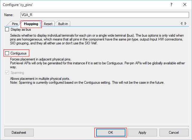
Right click on the pin and select "configure".
We only need to change the name to VGA_R, this time we will change the number of pins from 1 to 3.
Don't click OK yet.

Select the Mapping Tab and clear the Contiguous check box.
If that is selected, it will use adjacent pins when mapping them to the physical pin on the device.
That might be ok, but we rather have the flexibility to split them if we want.
Now you can click OK.
Repeate the same thing for VGA_G and VGA_B, or right click on the VGA_R select Copy, and paste to copies with the continuous pin checkbox already unchecked and the number of pins already set to 3, and just configure them to change the names to VGA_G and VGA_B respectively. You should end up with something like this:

Since we are limited on what memory we have on the chip (64KB) we can't have a huge frame buffer and use 9bits per pixel. So I'm going to choose just 4bits per pixel so we will have an rgb_out[3:0] with:
rgb_out[3] holding an intensity bit.
rgb_out[2] holding Red
rgb_out[1] holding Green
rgb_out[0] holding Blue
This is similar to the same approach systems on the 80s dealt with the lack of resources for computers back then, but we do have the same limitations with current MCUs so the methods used back then apply to this mid-end MCUs.
We will get back to the rgb_out wires in a bit. Since we are going to display a pattern, we need to control when to let the colors through and when not (because during blanking we don't want to output any colors).
We have the blank_n signal that is low (0) when we are not supposed to display a thing, and goes high when we are supposed to display colors during the visible area.
To achieve the blanking we are going to use a Mux (Multiplexer). What a Mux does is it has multiple inputs (base 2, so: 2, 4, 8, 16, 32, etc) but only one output. That output is selected via a control line that matches how many bits it needs to match that selection.
So for 2 inputs you just need one bit (values 0 or 1)
for 4 inputs you need 2 bits (00b, 01b, 10b, 11b) well in verilog the would be (2'b00, 2'b01, 2'b10, 2'b11 <format is: bits'base(b:binary,d:decimal,...)value in that base>) but we are digressing. Back to the Mux.
We need only two inputs, one for blanking and one that will the the colors go through.
So lets go to the library under Cypress->Digital->Logic and select the Multiplexer and drop it in the canvas.

Right click and configure it.
We don't need to change the name and if you leave the default one no name will be displayed.
But let's change the number of input terminals to two and the width to 4 (since our rbg out values are going to be 4 bits per pixel) But after we are done, you can experiment with the project and use all 9 bits to display all the colors possible, but I don't want to deviate for the goal to use the limited frame buffer.
Click OK, also don't forget to save all.

On the output of the Mux (which is 4 bits wide) we need to put a floating wire (actually a bus)
In order to do that, select the wire tool, click on the canvas where to start the wire, and click again where to end the wire. Once done it will automatically changed it to a bus because the output port is 4 bits wide.
The reason we start away from the pin to create the floating wire, is that if you did it the other way around, you can't click on the empty canvas to end it.
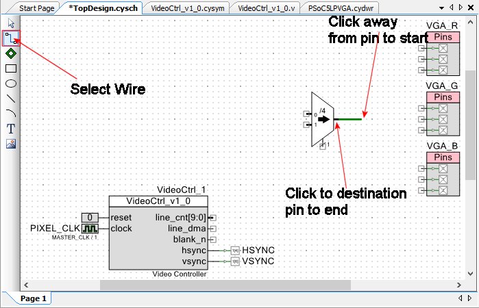
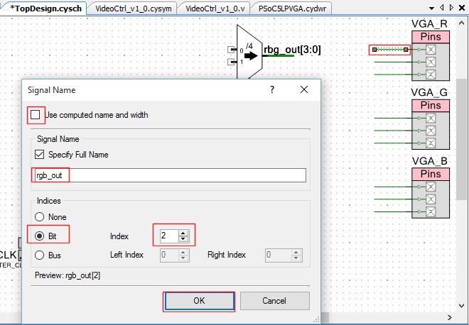
We are not done with that wire. We need to name it because later on we need independent wires of that bus to connect to our rgb outputs.
You can double click on the wire, or right click on it and select "Edit Name and Width"
On the dialog, uncheck the "Use computed name and width"
Change the name to "rgb_out"
We can leave the rest alone.

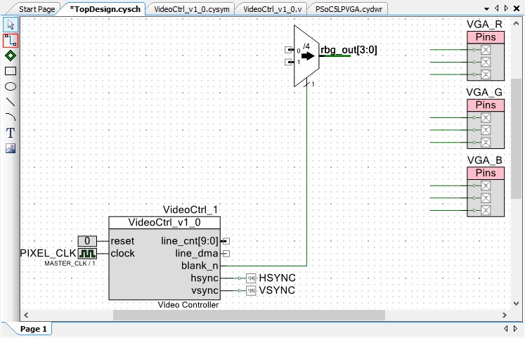
I'm going to speed this up a bit for the following wires, create floating wires for the VGA pins.
You can move the Mux out of the way, also you can click on the rgb_out[3:0] wire name and move the label from the default location.
Also go ahead and connect the Mux control to the blank_n signal
Now we are going to rename those single wires.
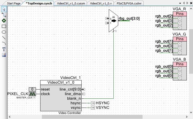
This is an image of the first one, we are going to select a single line from the rgb_out.
bit 2 corresponds to red.
Do the rest so it looks like this (you can also select the 1st one, copy and paste then rename them as needed):
RIR GIG BIB, the intensity (I) applies to all three channels to boost the color.
On the Mux, when the value is 0 we want to blank the rgb_out, so we need to add a 4bit wide 0 digital constant:

It's 8 bits wide by default with the value 0xff (255) we need to change the width to 4 bits and the value to 0.
Right click on the constant and select configure.
Change the value to 0 and the width to 4.

Lets add a floating wire to the line_cnt[9:0] pin, remember to start away from the pin, then click again on the wire and select "Edit Name and Width", uncheck the "use computed name and width" and change the name to "line_count"

Remember you can select the label and move it around to make it look better.
Save all! (I shouldn't say this anymore but it's important to save your work).
All that we have done so far, we are going to keep on the future progress of the project.
But just to display something we are just going to select 4 bits from the vertical line counter. Not too exciting since the line value remains constant through the whole line, but since it's temporary it would be easy to do and undo and we get to see some video on our VGA monitor

So add a floating wire to the remaining input pin in the mux.
Rename it line_count[3:0] (so it's 4 bits wide as needed). This will change the color every line since we are using the lower 4 bits. If you instead use line_count[4:1] it will change color every 2 lines.
[5:2] (still 4 bits wide) will change color every 4 lines, etc until [9:6] wich will change colors every 2^6 lines (64).
You can copy and paste the 10 bit one from the device, connect it, move the label out of the way and change the indices on the copy.
We are ready for some video, but first let's look at least at the red channel on the scope.
Save all and compile it.
(Oooops) I misspelled my Mux out wire, change the name to r
gb_out. And compile it again.

Also we need to assign the pins for the VGA RGB pins. So go to the PSoC5LPVGA.cydwr and assign them there.
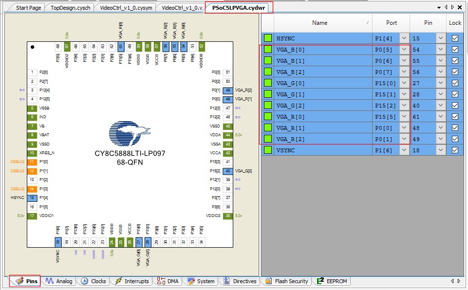
Note that I'm using pins 15[0] and 15[1] amongst my selection, Those two are important because if you want to use an XTAL you have to connect it there, so you will have to move your Green signal to some other pins.
Also P15[2] and P15[3] are use for the Real time low frequency XTAL if you need a 32.768KHz accurate RTC clock for other features.
I do have that VGA to BNC adapter so it's easy for me to probe the signals.
On my scope I'm going to trigger on VSYNC (Black Cable of the VGA to BNC) via the external trigger (I only have a two channel scope), Then Channel 1 is going to have the HSYNC (White BNC cable) and Channel 2 is going to have the Red channel (well... Red cable).
Program the device and let's see what we see in the scope. I have the trigger delayed by 1.2ms so we clear all the blanking area. Channel 1 for the HSYNC set to 2V per division (Since it's TTL 0V-5V) And Channel 2 for the red at 500mV per division, since the range is 0V - 0.7V, I do have my ratios set to X1 and the timing to 200us per division.
The actual pattern doesn't correspond to the final output, but the voltage levels are right, I had the pins mixed up and it's late so I'm not going to take another set of scope captures.

Things look good, let's take a close up at the 4 red levels, we are well under 1V which is considered safe for VGA signals, and I'm not using a 75 Ohm terminator

Here it is with a 75 Ohms terminator.

I did also check the Green and Blue signal and it's all within spec, so let's see what we get on the screen.

I did find some small timing violation that I'll investigate later, but, Yeah! we have video!
I added the Zip file of the project so far to this point.
------------------------------------------------------------------------------------------------------------------------------------------------------
External clockOptional: Using DSI Signal as a precise Clock Input
The internal oscillator is not the most precise way to generate a pixel clock. The problem with that is that on the video you'll see some horizontal banding and some video tearing depending on the video resolution and what is displayed on the screen. Meaning if every pixel is a different value you will see more noise in the output image.
PSoC 5LP supports two alternatives to the IMO (Internal Main Oscillator) as a clock source.
The first one will be the use of the MHz ECO (MHz External Crystal Oscillator) supporting both crystal resonators and ceramic resonators in the 4-25MHz range.
There is also a kHz ECO for a kHz clock domain but that's more for a real time clock (RTC) which we don't use.
More details about this first option that we are not going to use here can be found in this cypress app-note:
http://www.cypress.com/file/141216/downloadThe second option is to use the Digital Signal Interconnect (DSI) in the 0-33MHz range. This is the optional method we are going to implement, and more details can be found on this app-note:
http://www.cypress.com/file/140916/downloadI do have a 26MHz OCXO that I'm going to use. In it's simplest configuration you give it power/ground and it will spew a clock. You can trim the clock but that's beyond the scope of this tutorial. What we want is to show how to make use of an external signal clock (could come from another MCU or anything else that could provide a clock in that range).

The trimming is pretty much is a resistor divider and an inductor to clean the signal.
In my implementation I'm taking the external clock output of the OCXO into p3[0] of the dev board. But it could be any other port since the DSI clock is not restricted to any given pin.
I did choose this, because I didn't want to deal with using the XTAL, but the 1st method using a Crystal resonator is the best option because the OCXO consumes too much power and it's not cheap. A Ceramic Resonator like this one:
https://www.sparkfun.com/products/92This will be better than the internal one and easy to configure without needing load capacitors. I pointed to a 20MHz resonator because our target is 40MHz, but if you wanted to achieve other frequencies you would have to select an XTAL that the PLL could derive your target frequenc(y/ies) from.
As for precision:
Very low PPM use OCXO or other temperature controlled oscillators or any other external clock via DSI.
< 1000 PPM use a Crystal Resonator adding load capacitors via XTAL.
< 50000 PPM use a Ceramic Resonator with built in load capacitors XTAL.
> 100000 PPM (1%) using the internal main oscillator (IMO) will be fine.
You can have one or more implemented and select the input clock later on. On this tutorial we are going to define the DSI clock at 26MHz, because that is the OCXO I have around, but I will leave the project to use the IMO.
Ok, time to bring that DSI clock into our project. For that we just need to bring a digital input pin to our schematic (To be found in the component catalog under Cypress->Ports and Pins.
Name it DSI_CLK_IN by right clicking on the input pin and selecting configure. Also go to the Input tab and set the Sync mode to be Transparent, because you can't sync on the input clock with the master clock that is derived from it. Note: I left the Drive mode under the General Tab, to be the default "High impedance digital".

Create a wire to it and name the wire dsi_clock_in

Also go to the .cydwr tab and assign the DSI_CLK_IN pin to the right port (in my case P3[0] on pin 29.
Let's configure the Digital Signal, for that you need to open the .cydwr file, click on the clocks tab, double click on the yellow area to bring the system clocks configuration, then enable the Digital Signal check mark. Open the "..." to select the source clock. select the dsi_clock_in signal and type the external signal frequency. I'm leaving the Accuracy at 0% (as in perfect), click OK.

Now on the PLL you can select the input from the IMO to the Digital Signal. I will leave the 2nd zip of this post to use the IMO but you can change the input clock for the PLL in here, this will change the Master Clock and the Bus clock as well but our desired frequency remains unchanged.

This is a capture using the IMO at 3 MHz with just 1% accuracy 17.6 ms after the vertical sync trigger with infinite persistence on to show the jitter (12us) just one video frame after the trigger.

This is a capture using the external OCXO after 60 frames (almost a full second after trigger) with infinite persistence showing no jitter at all.

---------------------------- Non optional update -----------------------------------------------------------------
Since I'm updating the code, I'm changing the h_count_r in VideoCtrl_v1_0.v to have 11 bits:
reg [10:0] h_count_r;
Reason being is that if we try to use a horizontal 1024 visible mode, the 10 bits were not enough, so with this change we can handle up to 2047 horizontal visible lines.
Code for the counter is 1 based, to optimize when we reach the count, because I didn't want the module to require placing a 0 based pixel value, I could have added a constant but that would eat resources that we don't have.
Also we are going to change the temperature constrains (Thanks to Stephen AKA skench for finding this out) from Industrial to a commercial range. That could have been resolved by optimizing the Verilog mapping to the system resources but for this tutorial this is a good enough solution, so we can't operate now from -40C to 0C, oh well.

Updated code on Archive05 zip file attached.
Support images for this part of the update are going to be on the post with the update, since there is a limit of 25 files per post.


