Author Topic: Questions on JLCPCB  (Read 2370 times)

0 Members and 1 Guest are viewing this topic.

Offline criznachTopic starter

  • Newbie
  • Posts: 8
  • Country: us
Questions on JLCPCB
« on: July 30, 2018, 05:38:17 pm »
I've ordered a few things from JLC with decent results and am looking to try a more complex, PCB artwork design.  I'll need routed, curved outlines and some slots.  And I'd also like to be able to hand-solder some SMD LEDs on the board's edge.  So I have some questions...

  • It looks like 2mm is their routing width based on their capabilities page.  Can they do smaller, and/or does it cost more?  I was hoping to make some 1.6 (or so) slots for joining boards.  If I can only get 2mm, I'll wiggle or zig-zag the slots to make 1.6 fit tightly.
  • If I ignore DRC errors, can routing go through a copper pour or pad?  I'd like large-ish pads at the slot edges for joining boards together at 90 degree angles.
  • And again, ignoring DRC errors, can I cut plated holes (both round and oval) in half with the edge routing layer?  This is how I planned to edge-mount SMD LEDs.
  • If I omit the solder mask over an area on both sides, does the PCB material appear brownish?  It's hard to tell from the boards I have with full solder mask.

Thanks!
 

Offline innkeeper

  • Supporter
  • ****
  • Posts: 615
  • Country: us
Re: Questions on JLCPCB
« Reply #1 on: August 04, 2018, 03:00:43 pm »
think that's a question best asked directly to JLPCB.

If you get an answer from them, please post. It is good information to know.
Hobbyist and a retired engineer and possibly a test equipment addict, though, searching for the equipment to test for that.
 

Offline TheUnnamedNewbie

  • Super Contributor
  • ***
  • Posts: 1208
  • Country: 00
  • mmwave RFIC/antenna designer
Re: Questions on JLCPCB
« Reply #2 on: August 04, 2018, 03:56:42 pm »
Quote
If I ignore DRC errors, can routing go through a copper pour or pad?  I'd like large-ish pads at the slot edges for joining boards together at 90 degree angles.

That sounds like it is not really a DRC error in the eyes of the manufacturer. Even in most PCB tools you can turn that off so it is not a error by for example connecting the pour or pad to the same net as the routing so it no longer counts as a 'short'.

Quote
If I omit the solder mask over an area on both sides, does the PCB material appear brownish?  It's hard to tell from the boards I have with full solder mask.

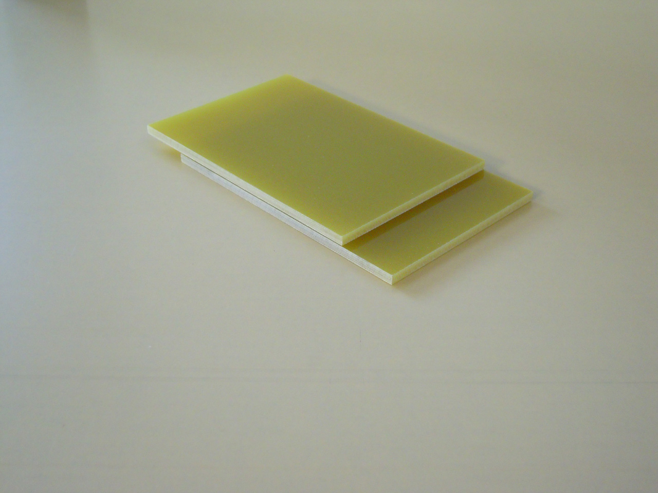
Do you mean over copper or over bare substrate? Substrate is usually FR4, and I don't think JLC can do anything else (at least not for their cheap 2 dollar boards). It should look like any other FR4, and will be something similar to this:


Source: http://www.gar-fond.com/english/unclad-fr4.html

As for the other two: You should contact the manufacturer on this.
The best part about magic is when it stops being magic and becomes science instead

"There was no road, but the people walked on it, and the road came to be, and the people followed it, for the road took the path of least resistance"


Share me

Digg  Facebook  SlashDot  Delicious  Technorati  Twitter  Google  Yahoo
Smf