I figure I'll close this repair up and condense a bit of the measurement info - in case someone's got a 6GHz extension board with problems and want something to compare it to. I've also made a bunch of measurements to show the value of shielding (if anyone had any doubts...) that are at least neat looking, but since it's a lot of images and a few that I want to combine, it will take a bit more to put it all together. Long story short, you get a little bit of a broadcast on frequencies below the crossover to use this board, but then you get basically everything when the frequency is coming from the uncovered board - and at least from an initial glance, you can see the harmonics come and go as the frequency rises and the filter bands are engaged. The harmonics on the output also drop something like 20dB as a baseline, and in most cases much better than that, and just by sticking on the shielding bits, the board essentially becomes silent - the chassis doesn't seem to contribute much to shielding, since every unit is self contained in a shielded box.
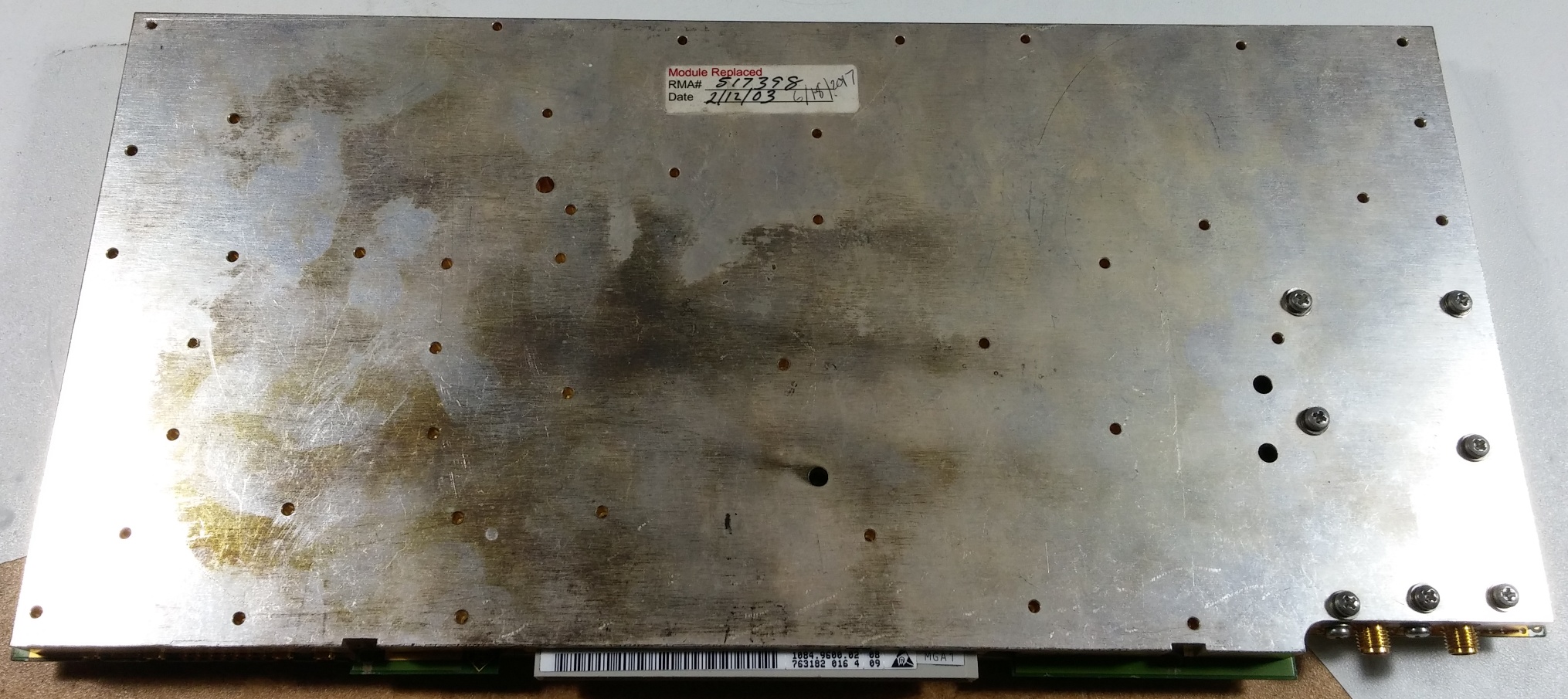
So from that last post proclaiming it fixed, I removed the card, removed the mod wires, replaced N3 with the same chip as N4, cleaned up a couple of odd looking joints from previous mod wire removals, and then sprayed down the flux residue with my fancy alcohol sprayer (airbrush). Did a pretty reasonable job cleaning it, though I never had the guts to clean the hybrid power module with alcohol and was sure to wait after soldering (warm ground plane + fast evaporating alcohol in an airstream seems like a recipe for thermal fractures...). And I was left with this nice clean board:
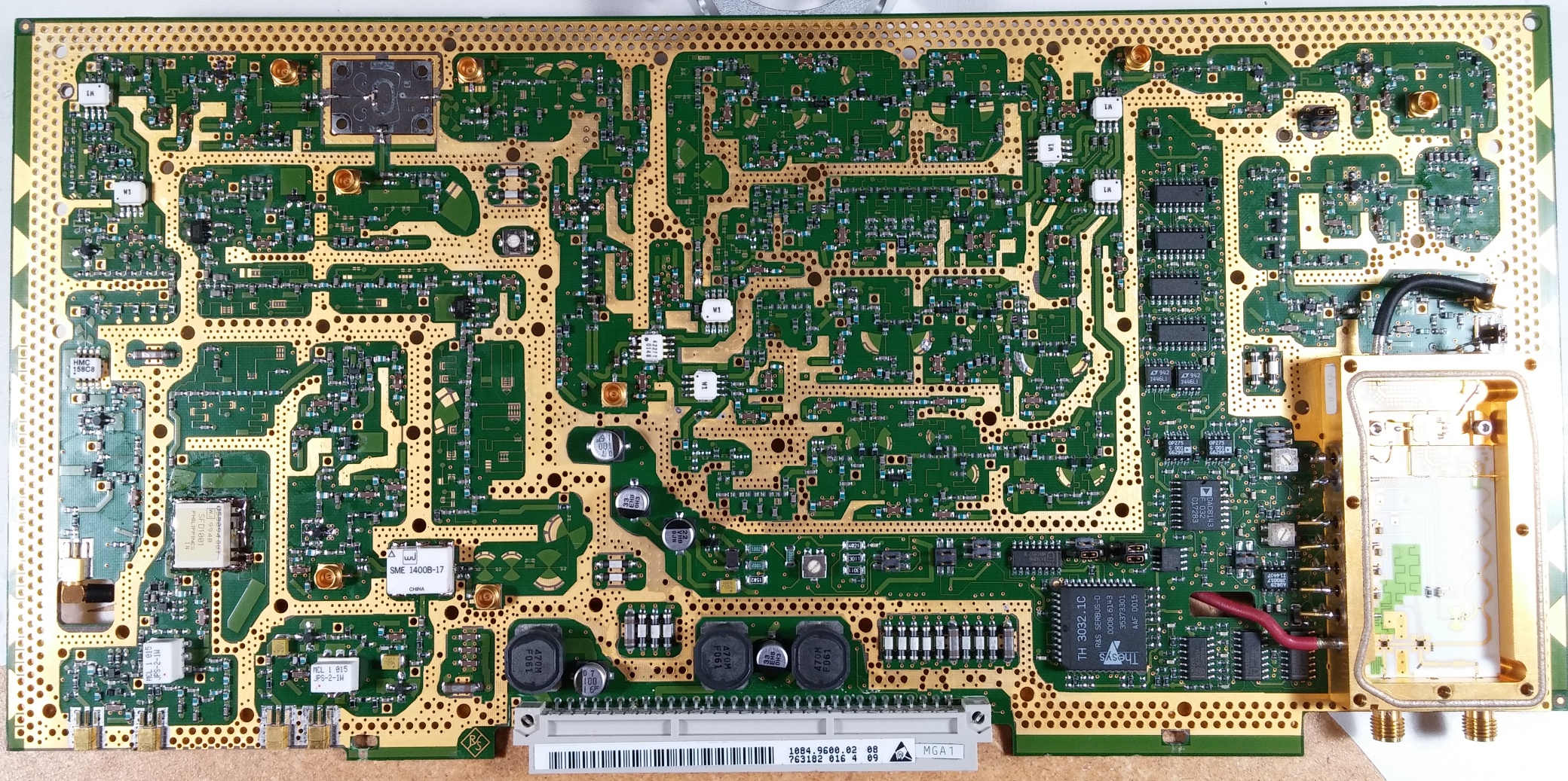
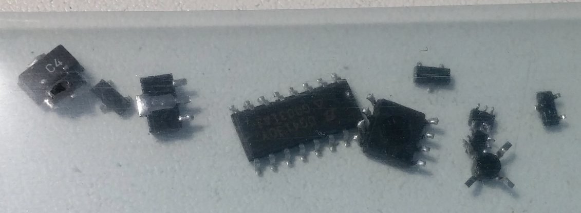
Over the last month and a half, I replaced all these parts.... though in retrospect and after seeing the fixed failure... several of these are probably fully functional

I put it back in and ran some tests for the sake of interest, then pulled it one last time to put it all back together. I found that the silver tarnish came off the shielding very easily with a little rubbing alcohol, so I went around the edges and the RF gasket to try to make sure the seal was good, then I clapped on the two shielding boards and went to town on something like 40 torx screws.
Then back in the box with the others, making sure the SMAs were nicely tightened:
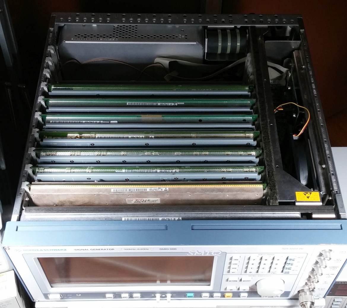
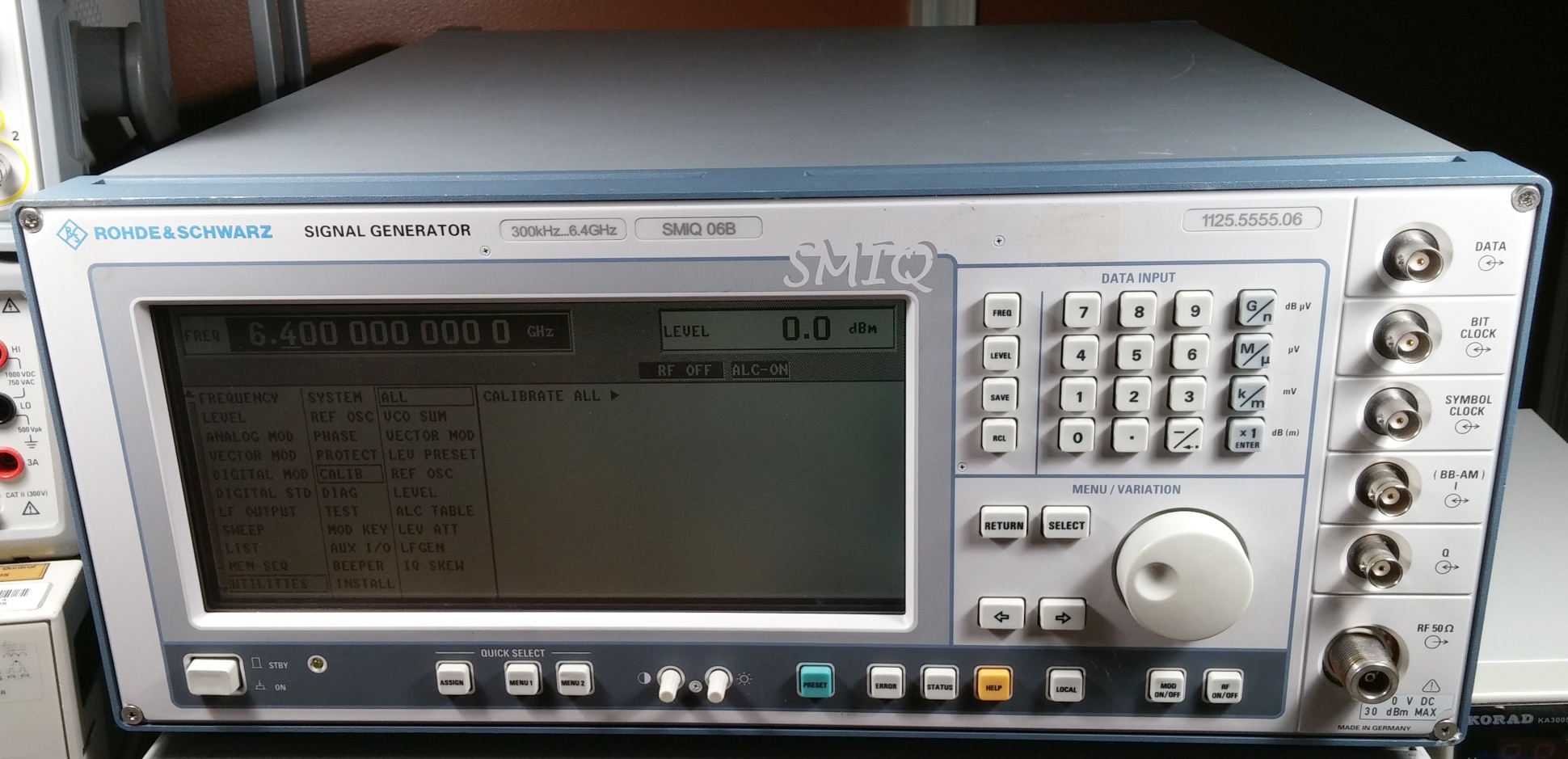
Then after some testing, I slapped on the top and bottom housings and put on the back pieces... for a nice looking piece of functional test equipment.
When it was fully together, I left it and the RF power meter on for a bit, ran the full self calibration of the SMIQ and zeroed my sensor and checked output linearity... it got a bit better! At the bottom end, it's a bit under, I saw as far off as -0.23dBm when the output was set to 0dBm, but for most of the range it's off by only a few hundredths of a dBm, and right at the top it was +0.03dBm. Quite pleased, especially given that the sensor's last cal was probably in the late 90s.
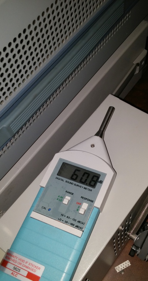
Also took a measurement of the sound level, at about the same positioning as before, and it's somewhere around 4.5dB down! It's honestly higher than I expected from the reading, since it sounds much quieter to me, but getting the chassis on did get the noise up a bit. Now instead of being pretty much the noisiest thing on the bench, it's under the stock fan for my DS4024 and my power supply takes the loud-operation crown once again.
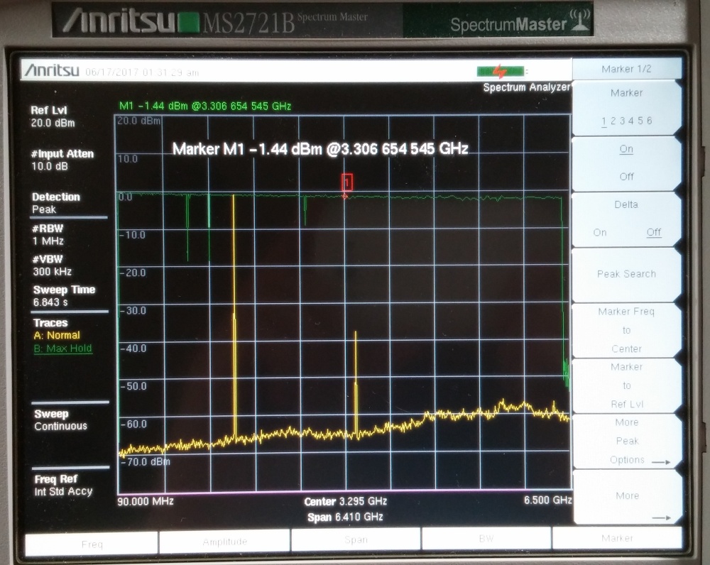
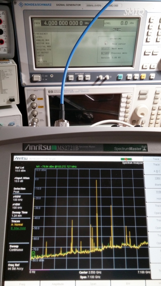
I took a nice long peak hold run of a frequency sweep output to get a general idea of linearity of the output (and I actually think the dropoff shown is more in the spectrum analyzer, since the cable should be fairly good and the power meter reads a lot less than this). Regardless, it looks much better.
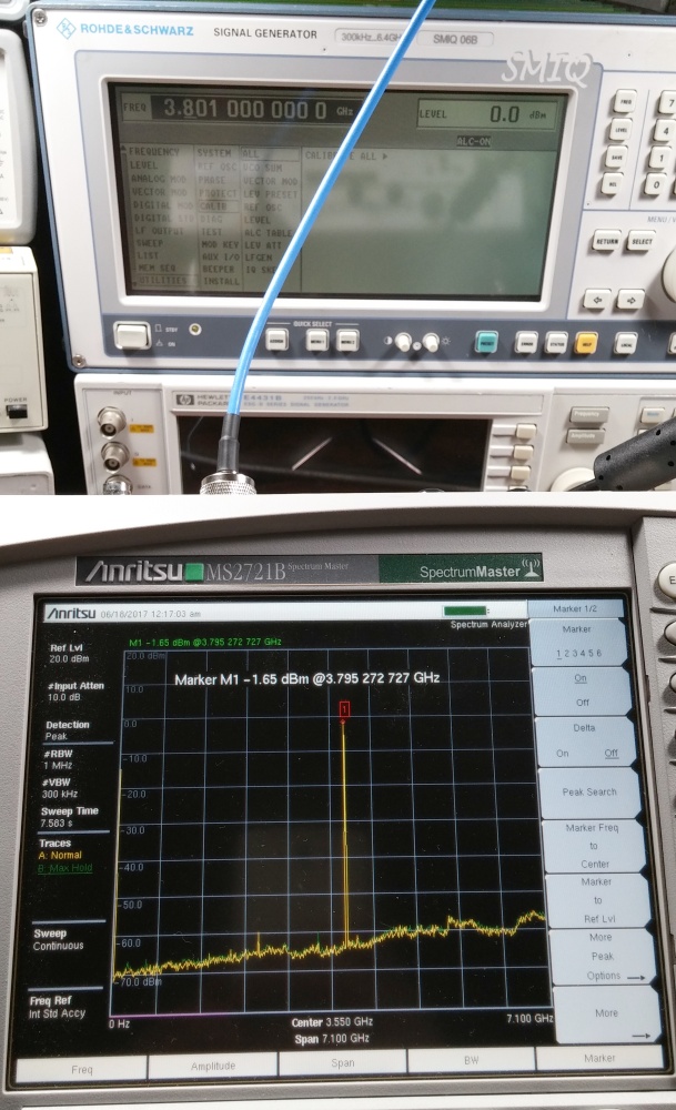
And while I'll go into the EMI readings later, even though the frequencies are slightly different, this gives you an idea of the noise reduction you get on the output with nice shielding. With the shield @3.8GHz:
Without the shield at 4GHz (same frequency band, didn't remember to actually match the frequency or the RBW... but the trend is clear)
And to aggregate, I sent along the test point readings and are in the spreadsheet in the last post - these are accessible through the menu without opening the unit at all and without external gear. And here's the measurements I noted down on the bias lines for the RF amps and some other things - always 2 inductors away from the signal path. My board reports as Var. 2, Rev. 2 in the software, and it is somewhat different from the schematics (most of the "not populated" amps in the schematic are present. I didn't note frequencies for most of them and I know frequencies changed somewhat (and a few intentionally are driven differently with frequency) so use these as guidelines, not necessarily correct values for your situation.
MGA86523 amps:
N14 - 3.125V
N25 - 3.133V
N35 - 2.784V
N36 - 3.959V
N37 - 2.905V
Other types
N38 - 4.913V, somewhat noisy
N39 - 4.906V, somewhat noisy
V20 - 4.457V, somewhat noisy
N15 - 4.537V
N17 - 4.513V, "chunky" noise (similar amplitude, but slower changing)
N4 - 6.612V-6.601V,
THIS MEASUREMENT WAS TAKEN WITH THE FAULTY AMPN3 - 4.72V-4.69V, gradual drop as it warms up
THIS AMP WAS ALSO REPLACED AS A PRECAUTIONV87 - 4.423V, varies with level adjustment
V91 bias: 4.71V
V92 gate: -1.35V
V92 bias: 7.133V
V94 bias: 7.05V
V95 bias: 7.05V
V191 gate: -5.039V
Power module VDD: 7.2V
It's also worth noting that the faulty N3 did not measure any differently from N4 when removed from the board using a multimeter's diode check function even though it was clearly the fault. A number of diodes and things read really strange testing this way in circuit, even when the circuit seemed very simple, only to be fine and consistent when removed.
Some RF noise investigations to follow to round out my work in the unit.


