Author Topic: Anatomy of a Fitbit One  (Read 3500 times)

0 Members and 1 Guest are viewing this topic.

Offline AdlerTopic starter

  • Regular Contributor
  • *
  • Posts: 62
  • Country: ca
Anatomy of a Fitbit One
« on: December 09, 2013, 06:21:38 pm »
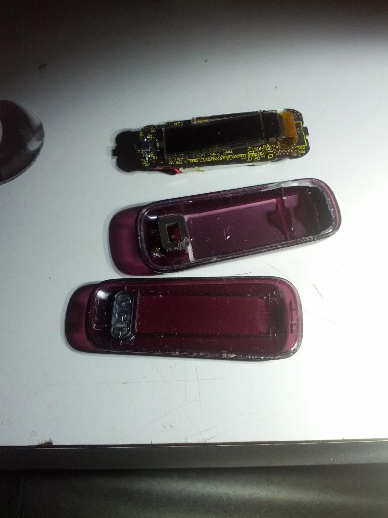
I had a dead Fitbit One and couldn't find any good pictures of it guts and components so I decided to see what this thing is made of. Not to mention evaluate its repairability (wasn't expecting much).

It was actually amazingly easy to get into the device. At first I tried prying on the metal back. This proved to be a mistake, the back is very well glued on and is entirely for show. The unit is comprised of two halves that when heated pried apart very easily.

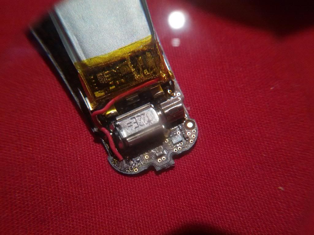
My first hunch that the battery was dead proved to be incorrect. Just in case, I swapped out the battery for a spare 3.7v lipo I had lying around. No change.

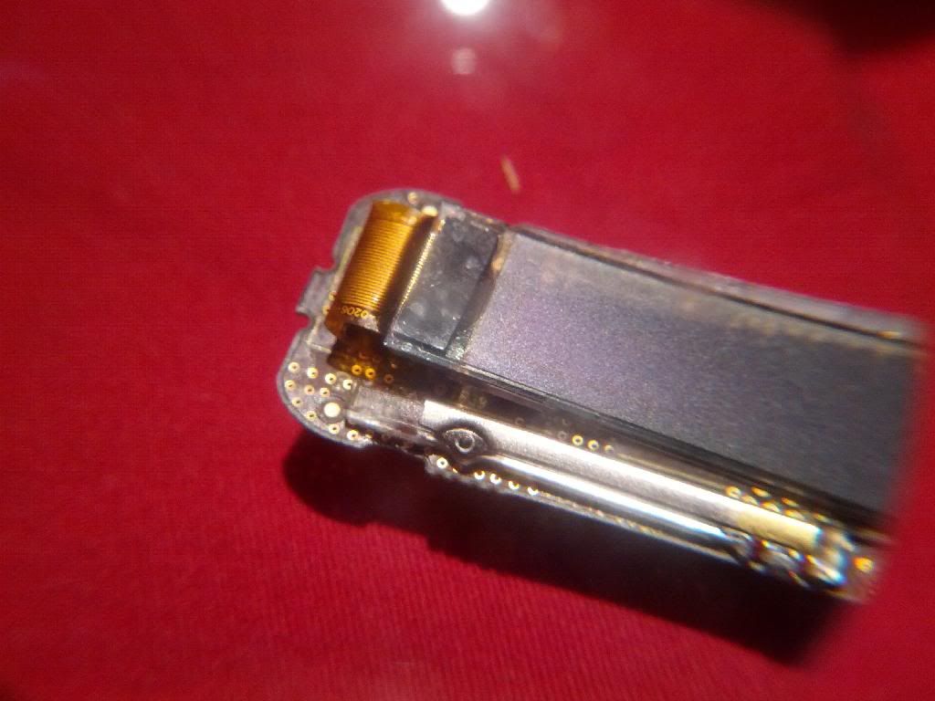
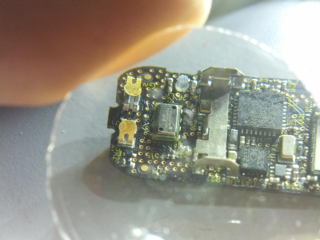
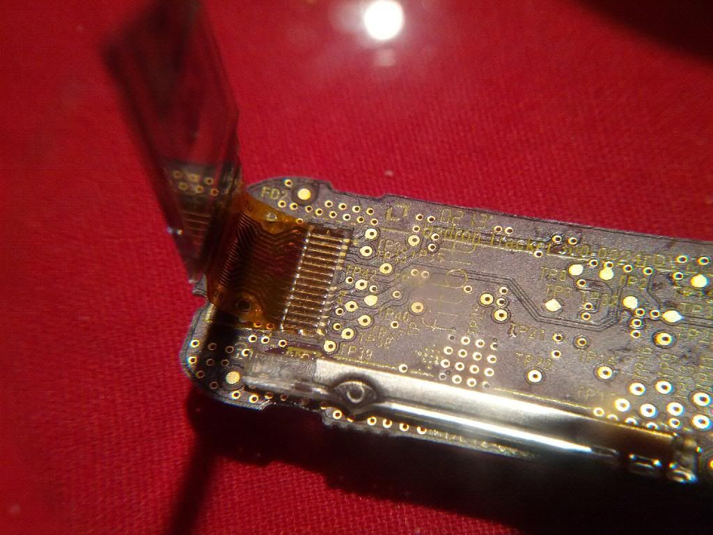
Turns out the problem is actually with the LCD (or something driving it). In some light at certain angles I can actually see the edge of the LCD displaying a picture but only at the edge and its insanely faint. I very much doubt I could source another LCD and if I could Im not too sure how these are connected to the board. If anyone knows please school me (Picture below. Doesn't look like solder, its just stuck down).

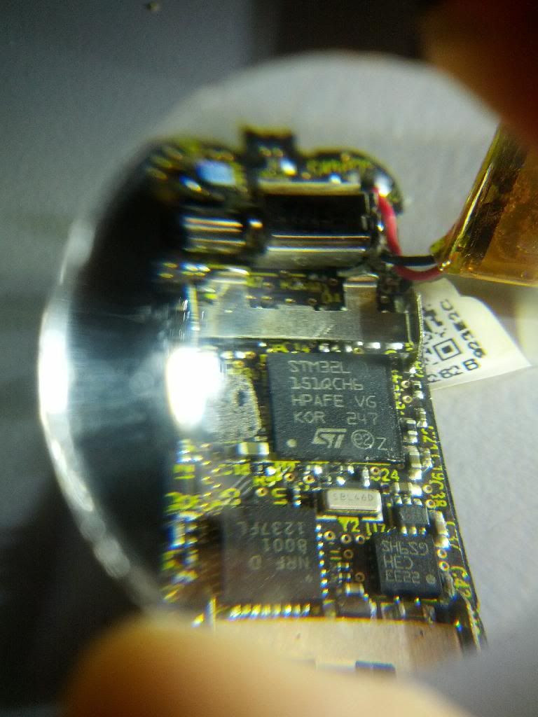
The processor is a STM32L ARM.
The bluetooth chip is a nRF 8001.
Regular old buzzer for the silent alarm.
It has a 560702ba03 digital pressure sensor. I assume for the altimeter?
Im not sure which chip is the accelerometer. Maybe the device next to the bluetooth?


Here are a slew of pics.


Offline thejosheb

  • Newbie
  • Posts: 2
  • Country: us
    • AquaPic Build Log
Re: Anatomy of a Fitbit One
« Reply #1 on: December 09, 2013, 07:22:08 pm »
Thanks for posting this. My wife got me one of these and I was really curious what was inside but she'd kill me if I tore it apart.
"Young Player". Designing a aquarium controller. Check out my build log https://sites.google.com/site/aquapicbuildlog/
 

Offline amyk

  • Super Contributor
  • ***
  • Posts: 8270
Re: Anatomy of a Fitbit One
« Reply #2 on: December 10, 2013, 12:29:04 pm »
The connection is made with anisotropic conductive film. The failure could be caused by separation of this - have you tried (gently) applying pressure on the ribbon where its bonded to the display, and also where it meets the PCB?
 

Offline AdlerTopic starter

  • Regular Contributor
  • *
  • Posts: 62
  • Country: ca
Re: Anatomy of a Fitbit One
« Reply #3 on: December 12, 2013, 12:31:21 am »
The connection is made with anisotropic conductive film. The failure could be caused by separation of this - have you tried (gently) applying pressure on the ribbon where its bonded to the display, and also where it meets the PCB?

Interesting stuff. I have tried all kinds of pressure on the ribbon, nothing works. I am considering peeling up a small portion and trying to melt some solder paste in the junction. I'm not sure the ribbon can handle the heat, we'll see.
 

Offline amyk

  • Super Contributor
  • ***
  • Posts: 8270
Re: Anatomy of a Fitbit One
« Reply #4 on: December 12, 2013, 12:33:32 pm »
I'm not sure the ribbon can handle the heat, we'll see.
No. That's why ACF is used.


Share me

Digg  Facebook  SlashDot  Delicious  Technorati  Twitter  Google  Yahoo
Smf