Here's another entry in the engineer-with-no-job-security-and-a-screwdriver series (
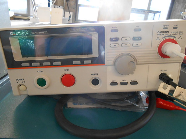
https://www.eevblog.com/forum/reviews/elgar-3000b-(ancient)-ac-line-conditioner-teardown/): this time I pulled the cover off a hipot tester. These are meant for verifying voltage-withstanding ratings (such as between the primary and secondary sides of a transformer) and measuring insulation resistance, in both cases by applying a high voltage and measuring the (hopefully very small) current that flows through the insulation. This particular model can apply both DC, from 100V to 6kV, and sinusoidal 50/60 Hz AC, from 100VAC to 5 kVAC (=7.1 kV peak?) to the insulation under test.
Here's the view of the inside:

There's a few boards in here, all connected with a good number of cables. At the back end, the AC line comes into a board I'll call the "back board", with some power supplies on it. Just forward of it is another board I'll call the "front board", which also has some power circuitry. Attached to the front panel is a control/measurement board. There's also a board directly underneath it, on the backside of the front panel, which drives the LCD and buttons but that's not too interesting so I'm skipping it (plus lots of disassembly work). Over at the right are the best bits, a high-voltage transformer and a couple high-voltage boards which connect to the output.
The "back board" has...
* An EMI filter for the AC line,
* A bridge rectifier peak-charging a couple big aluminum caps,
* An aux-supply flyback driven by a Power Integrations chip, with a few outputs which get filtered and run to the control board,
* Another DC-DC supply, with the white-plastic-cover chip driving a noticeably larger transformer, which feeds a couple well-heatsinked diodes and a couple aluminum caps.

The "front board" has a bridge rectifier with a couple fuses and a MOV feeding some hefty bulk caps and a two-transistor power converter of some kind. Since the manual brags about using a PWM inverter to avoid variations in the AC line feeding through to the output, and there's no diodes here on the output, I'm guessing that this is the PWM inverter which generates a 50 or 60 Hz sinewave. The large passives next to the transistors are likely for filtering. Also notice the unpopulated spot for a fan on the right.

The output of this board actually runs back to the "back board", where it seems to get switched by a relay and sent to the primary of the high-voltage transformer.
Here's the control board: linear regulators for the various power supplies are on the right, digital controls are in the middle, and the measurement section seems to be on the left:

It's controlled by an MSP430 microcontroller and some kind of Lattice programmable-logic device:

Close-up of part of the measurement section, with what appears to be multiple current sense resistors (330K) and ranging relays:

The transformer and high-voltage section are pretty interesting. Here's the label on the transformer:

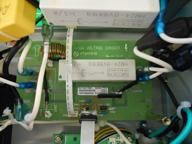
...while the rest of the high-voltage section consists of two stacked board, full of swiss-cheese cutouts for creepage:

Notice the two power diodes on the top board connected in series, and the three diodes on the bottom board connected in series:

There's also an 8kV film capacitor:

...and some seriously-high-voltage reed relays (the white boxes).
Now how does it actually work, you say? I was very confused by some things about the interaction of the "back board" and "front board", so I went probing around and drew a block diagram of the input side / schematic of the high-voltage side:

Let's start with the input side. The DC-DC on the "back board" takes the rectified AC line and steps it down (judging from the ratings of the output caps). This lower DC voltage then gets fed to the sinewave inverter, which drives the high-voltage transformer primary. The part I was confused about is why the DC output goes through an MOV and bridge rectifier, and why there are such large bulk capacitors on the "front board" when the "back board" has its own decent-sized buffering caps. All these things don't make sense from a regulated DC output, and very much feel like it's supposed to connect to the AC line. The only explanation I can think of is that the "front board" is either:
1. A 3rd-party product that they dropped in to save development time, or
2. A board from a different GW Instek model, which has a fixed output voltage and so is meant to run directly off the AC line. In this case it could probably vary the PWM duty cycle a bit to regulate the output.
There's also the question of why you'd have a DC-DC feeding an inverter, when the inverter can already scale its PWM duty cycle range to change the output amplitude. I think this is about control range: if 6 kVpk output = 100% D at max. (ignoring overhead for regulation), then the min. rated output of 100 Vpk = 20% D at max. With a max. D of lower than 20%, as the sinewave descends from the peak, duty cycles quickly get small (<= 5%); at these levels, the timing of the controller and gate drivers (minimum on/off times) and dead-time are more critical. Doing a 1-stage design would be completely doable, but definitely more difficult to develop. Decoupling the sinewave generation from the input level control makes the design a lot easier and more flexible.
Now, on the output side, there seem to be two parallel paths, selected by relay. The output secondary is clamped against overvoltage (for stored leakage energy if the power shuts down not at a zero-crossing, I'm guessing) by the triple string of TVS diodes. Then, depending on whether the AC or DC-selection relay is closed, the transformer voltage either passes through a filter inductor and directly to the output (AC path), or gets half-wave rectified and buffered by the high-voltage film cap before getting sent to the output (DC path). There's also a voltage divider made up of very long high-clearance/creepage 10M resistors on the output, used to sense the voltage and send it back over the flex cable to the control board. The return path for the negative output terminal comes back through the control board, which is likely where it senses the output current.
Let me know if you have any questions.


