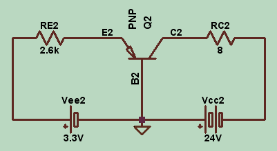
Analysis of the questionFirst, there is an error in one of the formulas (maybe introduced with the formatting of the original question), but I see that everybody here has automatically intepreted what the student meant, nevertheless (I wrote this part before Kleinstein spotted it). He wrote "V2 = VE - VB" instead of VC - VB and there is also a question of signs (VC - VB or VB - VC?) that might be discussed but from the actual question asked it seems clear that the student is talking about absolute values.
I have to disagree with the conclusion reached by rfeecs that we cannot say V2 > V1, because the drawing, as ugly as it is, shows that the battery that is reverse biasing the collector junction is bigger than the one forward biasing the emitter junction. This is the classical circuit configuration used in several textbooks to explain how transistor works and it is implied that the transistor is in active mode. If VBE is at least 0.6V, then |VBC| is at least 0.6V. Now, this might seem to void the question of any meaning, since if we already know (from the batteries sizes) that the output voltage is in absolute value greater than the input voltage the question seems already answered. But it's not. What the student is grappling with is how is it possible that in the input mesh we have a current IE that gives rise to a voltage V1 and in the output mesh we have a smaller current IC that (never mind the sign for the moment) gives rise to a voltage V2 that is bigger than V1.
And this brings us to the interesting point of the 'resistances' Rpn and Rnp. A diode is indeed a resistor, albeit a nonlinear one as correctly noted by TeslaCoil (one reference to rule them all: Chua, Desoer, Kuh, "Linear and Nonlinear Circuits"). We are used to deal with the dynamic - differential - resistance of the device because our way to analyse nonlinear circuits is by linearizing them in the neighbour of their operating points, but this is not the case: here we are considering a large signal behaviour and the resistance (the value of the ratio V/I) happens to be a nonlinear function of the voltage (or the current).
The coexistence of these two similar but completely different concepts of resistance is nothing new: we do this for hFE and hfe when the relation between IB and IC is not linear, and in physics for phase and group velocity when the dispersion relation is not linear.
 https://i.postimg.cc/9MBpqFn2/Nonlinear-relations.jpg
fig. nonlinear relationships and global and differential quantities
So, the resistances the student is referring to are the values of the ratio V/I for a given voltage (or current). From the point of view of the input mesh we see a small voltage V1 associated with a current IE, while in the output mesh we see another voltage V2 associated with a current IC. And the student is puzzled: if IE>IC how can we be sure that V2 > V1?
In my view, there are several opportunities here: explain why IE > IC is actually IE ≈ IC, and then what is the mechanism that allows basically the same current to be associated with different voltages. I would even go further and add a source resistor to 'program' IE and a load resistor to 'pour the programmed current into' and show that I can get power amplification (in this configuration, it's voltage amplification).
Many interesting answers so far, and I am grateful to all participants. Some of the answers are quite similar to the one I had already written. free_electron makes a valid point about the doping asymmetry of the BJT but I feel that is a bit premature to discuss at this student's level. That could be the subject of a follow-up question by the student.
I will post my answer shortly (it contains parts that have already been put forward), after producing a couple of pictures. And then I will explain - in a separate post so that it can be moved if necessary - the second purpose of my question here (even if I have just been threatened in PM to "mind my own business" if I am "not a teacher". LOL
So, here's my idea of answer. I modified my initial stance adding some more detail of the inner working, but I am not sure it is a good idea for a student at this level. Excessive detail and still to many simplifications (like my completely ignoring the electron current going from base to emitter) might lead to confusion.
My take on the questionFirst: in this configuration and with the base junction directly biased and the collector junction reverse-biased, the transistor is in active mode. This means that the collector current is alpha times the emitter current, with alpha slightly less than one (typical values can be 0.95 - 0.99 and higher) and that means that even if the collector current is technically smaller than the emitter current, we can consider IC ≈ IE.
From this, the reasoning of comparing Rpn IE with Rnp IC, when IE ≈ IC and Rnp >> Rpn resolves in favour of Rnp IC > Rpn IE. (It can be shown how we can add external resistors to the input and output mesh to exploit the fact that the same current can go through different resistances to provide amplification.)
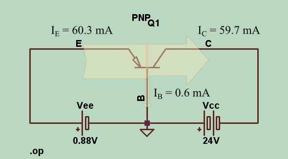
Here is the simulation of a fairly aggressive biasing using the simple default model of BJT in LTSpice. As you can see, even if they are mathematically different due to the relation IE = IB + IC, the input current IE and the output current IC are nearly the same - the differ by roughly 1%. For this example we can infer a value of alpha = IC/IE = 59.7/60.3 = 0.99.
 PNP BJT with ideal generators
The above explanation, though, is little more than a math trick because it does not actually explain why we can have basically the same current in both the input and output meshes when the resistances encountered can be so different.
The 'coupling-decoupling' mechanismSo, why is IC nearly the same as IE? And why, what
basically is the same current can have two different voltages associated with it?
It has to do with the dual mechanism of transport (
drift and
diffusion) inside a semiconducting material. Inside the copper conductors, the current is exclusively a drift current, where electrons are pushed along by the tiny (typically a few microvolt/m) electric field in copper. In the middle of the transistor, that is in the base, the current becomes a diffusion current that depends on the gradient in the concentration of carriers and not on the electric field.
If we focus our attention of the main contributors to the currents in a PNP transistor which are holes (see footnote), the oversimplified nitty-gritty details are as follows:
Inside the transistor, the current in the emitter is largely a hole drift current, acted upon by the tiny electric field in the bulk of the emitter region; the large number of holes that overcome the weakened voltage of the first depletion region cross the EB junction and, once in the thin base, they become a diffusion current that depends on the concentration of carriers. In the base, these holes are minority carriers that diffuse independently of the electric field and almost all of them - due to the geometry and concentration profiles - reach the base-collector depletion region, ending up in the collector bulk as if they were a reverse saturation current for the reverse-biased BC junction. We can call 'alpha' the fraction of carriers that from the emitter cross the thin base without recombining and without 'exiting' the base terminal.
In the bulk of the collector, the current becomes mostly a drift current again, this time subject to another electric field - the one associated with the small (we're talking mV, here) collector bulk voltage. The now majority carriers end up being collected by the negative collector terminal thanks to the electrons that are pushed there by the external circuit.
The large collector current is essentially an 'artificially inflated' saturation current for the reverse biased BC diode (in the VI characteristics, it is the nearly flat horizontal part of the exponential curve that sits right under the voltage axis) and, by being essentially independent on the base-collector voltage, it translate to the nearly flat horizontal output characteristics of the transistor.
As a matter of fact, a BJT transistor can be seen as a reverse biased diode (the BC junction) whose reverse saturation current is dictated by the carriers injected by the emitter.Here are the input and output characteristics of the common base transistor, along with the vertical characteristics of the generators, seen as one-ports attached to the BJT terminals:
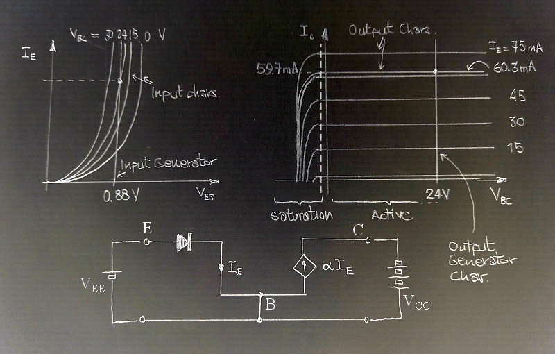 Input and output chars with ideal voltage generators driveHow is this 'coupling-decoupling' modeled?
The circuit under the characteristics is a large signal model for the PNP transistor drawn as a two-port: the input port sees a forward biased diode (the PN emitter junction), while the output port - with its horizontal characteristics at constant current (representing the reverse biased NP collector junction) - is modeled by a current controlled current generator.
To reiterate:
the fundamental mechanism that makes it possible to have a 'transistor action' is the existence of a 'bridge phenomenon' (diffusion) that is not ordinary conduction and that allows us to disjoint the effects of conduction current in the input mesh from the effects of (roughly the same) conduction current in the output mesh.
The need for diffusion as the main transport phenomena in the middle of the transistor is also the reason why we cannot build a transistor by putting two discrete diodes back to back, but that's another story...
Similar 'bridge phenomena' can be identified in the workings of FETs and MOSFETs. In all cases it is this 'decoupling' that allows us to model a transistor (in this example for large signals, but a similar reasoning applies to the linearized small signal circuits) with controlled generators - usually in a T topology.
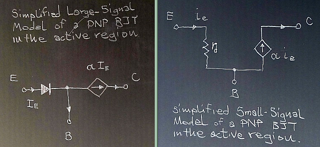 Large and small signal equivalent circuits of the transistor
We can turn this three terminal device into a two-port by putting one terminal in common, the base in this particular example.
And it is again the 'decoupling' between the input and output currents that allows us to either have amplification (in a CB configuration it is voltage amplification) or match impedances (the current that is paired with a large voltage in the output mesh is seen as a current paired with a small voltage in the input mesh).
Practical Application of transistor actionWhen the transistor is in active mode, the input mesh can sustain a maximum voltage, across the transistor BE terminals, of less than 1V (typically, it's 0.7V) and the input current is strictly linked to that voltage. The output mesh, on the other hand, can sustain the much higher voltages of a reverse biased junction, with a current that is essentially independent of that voltage.. Therefore, with an adequate supply, the output port can reach higher voltages than those provided in the input circuit. Since Ie = Ic + Ib, the current in the load will be roughly the same as that flowing in the input circuit. This simultaneous link between input and output current (they are basically the same) and decoupling of the voltages associated with such currents in the input and output meshes, is what makes amplification and impedance matching possible.
As a practical application of transistor action we can use an emitter resistor RE to 'program' the current in the input mesh, and then letting the transistor transfer it to the output where it can flow in another resistor, the load resistor RL.
How the voltage in the output mesh redistributes itself between CB junction and load resistor depends on how much voltage the current set by the input will develop across the load.
Two extreme examples are the following: in the first case we program a current of 3A in the input circuit by choosing RE = 0.78 ohm. The nearly 3A flowing in the load will result in almost all 24V of Vcc to drop across RL, and nearly nothing across the CB junction.
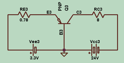 circuit 1: A load with big current and big voltage
Actual values for this circuit are
VEB = 0.98 V
VCB = - 0.45 V IE = 2.973 A Vload = 23.55 V
In this other circuit, where we program 1mA in the input circuit, only 8 mV will develop across the load resistor, and basically all of VCC will show up across the reverse biased CB junction.
 circuit2: A load with small current and small voltage
Actual values for this circuit are
VEB = 0.773 V
VCB = - 23.992 V IE = 0.972 mA Vload = 0.008 V @ 0.962 mA
The independence of the output current from the collector-base voltage can be easily shown by changing the value of the load resistor, without changing the 'programming' in the input mesh. For example, if in the above circuit we set RL = 10 kohm, we get nearly 10V across the load, 14V across the reverse biased collector junction,
VEB = 0.773 V
VCB = - 14.378 V IE = 0.972 mA Vload = 9.62 V @ 0.962 mA
and (with the idealized BJT model of LTSpice) the current did not even flinch.
Footnote:
What I am neglecting completely in the typical already simplified analysis of BJT currents that appear on introductory books, is the electron current that from the base goes into the emitter
This current can be made small by strongly doping the emitter and lightly doping the base. It's not exactly negligible but its inclusion would have complicated the exposition. Moreover, the "holes 'exiting' the base" are actually electrons entering the base and recombining with that 1% of the unlucky holes that do not make to the collector. In the charge controlled model of the transistor in a common emitter configuration, they are the reason a bigger current flows from emitter to collector.
...
I said that the purpose of my question was twofold, so I am going to state the second purpose in a separate post that happens to be post # 23.


