Author Topic: Help finding PCB design flaw  (Read 1065 times)

0 Members and 2 Guests are viewing this topic.

Offline mrburnsTopic starter

  • Contributor
  • Posts: 12
  • Country: fi
  • Automation engineer/coder. Electronics Hobbyist
Help finding PCB design flaw
« on: April 18, 2024, 10:44:10 pm »
My first PCB design with SMD components pre-assembled in pcbway went south immediately. (Magic smoke...)

The pcb is basically a breakout board for a Pi Zero to connect 20 DHT22 sensors, but with 3-5V to 5V boost converter for external power and selectable 3.3V or 5V sensor voltage.
- It also has level shifters for data lines coming from sensors to gpio.
- Attiny10 smd microcontroller to have full system and sensor reboot possibility.
- Place for dual usb-a connector with power on-off possibility.

I ordered 5 boards from pcbway with smd components and usb-c and micro-usb connectors assembled. I want to solder through hole stuff my self but I did not solder those yet.
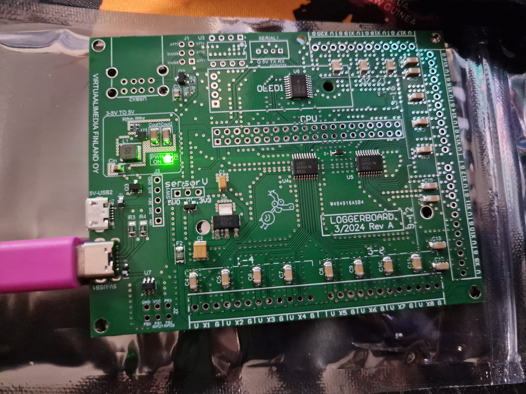
I just got the boards. Before powering on the first one I measured that nothing was not shorted and it looked good. Then I connected the usb-c connector to my phones usb charger.
1. First the power on led lit nicely and I was able to measure that the input was 5.125V and after the boost converter it was 4.999V. No problems. (The only thing consuming power at the pcb at this point was the small smd led.)
2. I then proceeded to carefully try to feel out if any component was overheating by just gently touching the top of the components. At this point the smoke came out of the feedback resistor of the boost circuit (Rfbt). (CRCW0402732KFKED CRCW Series 0402 0.063 W 732 kOhm ±1 % ±100 ppm/K SMT Thick Film Chip Resistor).
3. I disconnected the usb power immediately and started searching for shorts but found none.
4. I measured the second pcb for shorts and continuity on power traces.
5. I connected power to the second board thinking the probem with the first could have been a manufacturing flaw. -> Smoke from the input protection diode (D1) between the usb connector and the boost circuit.
6. I have been trying to find the flaw for two days now but cant find one. I already got smoke from third pcb and this time it was the p-mosfet (Q3) after the protection diode before the boost circuit.  |O
All help is appreciated.

Pictures:
https://1drv.ms/f/s!AnfIOtcTpP6Bg4Njyl16cHLvhViyuw?e=eCatYS

Link to circuitmaker project:
https://365.altium.com/files/C33BBF2E-E81A-4FCC-8011-A663D419CE9A

Project files archive: (corrected)
https://d3mo.fi/storage/Pi_zero_20sensor_2024_03_25/

What tools is have for debugging:
Fluke multimeters, lab power supply, frequency generator, soldering equipment, internet. :bullshit:

« Last Edit: April 19, 2024, 05:42:12 am by mrburns »
 

Online ataradov

  • Super Contributor
  • ***
  • Posts: 11272
  • Country: us
    • Personal site
Re: Help finding PCB design flaw
« Reply #1 on: April 18, 2024, 11:24:08 pm »
First of all, stop powering things from USB power supplies. Use a lab power supply with a low current limit.

Then attach your actual schematic. The schematic in the archive does not seem to match the board. In the Schematic D1 just goes to micro-USB connector. On the board it goes to both.

Wait, schematic is for a completely different board.
Alex
 
The following users thanked this post: mrburns

Offline mrburnsTopic starter

  • Contributor
  • Posts: 12
  • Country: fi
  • Automation engineer/coder. Electronics Hobbyist
Re: Help finding PCB design flaw
« Reply #2 on: April 19, 2024, 05:44:07 am »
Quote
Wait, schematic is for a completely different board.
Thanks for noticing. The I fixed the link to point to correct project archive.
 

Offline mariush

  • Super Contributor
  • ***
  • Posts: 5033
  • Country: ro
  • .
Re: Help finding PCB design flaw
« Reply #3 on: April 19, 2024, 07:55:13 am »
Some oddities in your schematic ...

VBUS of both usb connectors seem to be connected together, with no protection ... what happens if you have let's say a power bank on one port and a phone charger on the other...

There's switch ICs like TPS21xx you could have used (TPS2121, TPS2211 to TPS2115) you could use to switch between inputs,  there's ideal diodes you could use (ex LM66200 for dual ideal diode pack that auto selects highest input voltage, or single diodes like LM66100 that can be turned on or off with an enable pin to switch between two inputs)


Why use a tps61022 with maximum 8A switching current and an inductor good for 3-4A switching current, when the total power of your board is gonna be less than 500mA if you exclude the pi. Looking at max 2.5 mA for each sensor (if you read them all at same time), maybe 10mA per voltage translator chip, maybe 5-10mA for the microcontrollers...

The pi zero has it's own 3.3v buck converter on the board, you don't need to "stabilize" the 5v from usb, you're just doing a double conversion : https://datasheets.raspberrypi.com/rpizero/raspberry-pi-zero-reduced-schematics.pdf

Why the hell would you use possibly the shittiest version of 1117 regulator, that LM1117 needs capacitors with esr above 0.3 ohm.. you're using relatively expensive tantalum capacitors just to get this regulator working.

There's plenty of regulators that have very low dropout voltage and are stable with all kinds of capacitors ... some random examples just looking at highest stocked on digikey ...
AP7361C https://www.digikey.com/en/products/detail/diodes-incorporated/AP7361C-Y5-13/5638321 or https://www.digikey.com/en/products/detail/diodes-incorporated/AP7361C-FGE-7/5638318 ,

if 300mA is enough  AP2210K https://www.digikey.com/en/products/detail/diodes-incorporated/AP2210K-ADJTRG1/4470821 or AP2127K would work  https://www.digikey.com/en/products/detail/diodes-incorporated/AP2127K-ADJTRG1/4470788

for 500mA max, NCP8705 https://www.digikey.com/en/products/detail/onsemi/NCV8705MTADJTCG/5257920

You probably could have used a single buck regulator to convert whatever input voltage you have to something like 3.6v and run everything but the pi on 3.6v and use voltage translator if needed to change 3.6v signals to 3.3v for the pi)
« Last Edit: April 19, 2024, 07:58:51 am by mariush »
 

Offline mrburnsTopic starter

  • Contributor
  • Posts: 12
  • Country: fi
  • Automation engineer/coder. Electronics Hobbyist
Re: Help finding PCB design flaw
« Reply #4 on: April 19, 2024, 03:34:19 pm »
Quote
VBUS of both usb connectors seem to be connected together, with no protection ... what happens if you have let's say a power bank on one port and a phone charger on the other...
I was thinking this. But it would be good idea to add the protection if I ever order more of these. I just wanted both common port options so I would not need adapters with these.

Quote
Why use a tps61022 with maximum 8A switching current and an inductor good for 3-4A switching current, ...
I was thinking that if i need to attach a 4G/GSM Modem USB dongle or similar devices i would have enough power for them. Also I want to have option to use sensors and/or devices that draw more current.

Quote
Why the hell would you use possibly the shittiest version of 1117 regulator
I had no idea this is the shittiest version...  :palm: It would certainly be possible to use the Pi:s 3.3V but I have had so many problems with devices drawing too much from the Pi so I wanted to avoid that if I ever use 3.3V sensors..

Did you get any ideas what might cause the power problems when nothing is even connected?
 

Online ataradov

  • Super Contributor
  • ***
  • Posts: 11272
  • Country: us
    • Personal site
Re: Help finding PCB design flaw
« Reply #5 on: April 19, 2024, 03:40:47 pm »
Run it with a current limited supply and measure the actual current consumption. If it is high, eliminate sub-circuits and see what consumes that current.

The schematic is hard to read, but there is nothing obviously wrong, so you will have to debug it one part at a time.

Alex
 

Online MarginallyStable

  • Regular Contributor
  • *
  • Posts: 66
  • Country: us
Re: Help finding PCB design flaw
« Reply #6 on: April 19, 2024, 03:42:19 pm »
Not the problem, but "HOLY VIA's" around the regulator.
 

Offline mrburnsTopic starter

  • Contributor
  • Posts: 12
  • Country: fi
  • Automation engineer/coder. Electronics Hobbyist
Re: Help finding PCB design flaw
« Reply #7 on: April 19, 2024, 04:34:18 pm »
I have now found two things that might or might not have anything to do with the frying..

1. The MODE pin 6 is not connected to anything.
2. In the section 8.3 of the datasheet of the regulator is says "For those applications with input voltage higher than 4.8 V, TI suggests adding a diode between the VIN pin and
the VOUT pin to pre-bias the output before the TPS61022 is enabled. As an example shown in Figure 8-13, the
input voltage is from a USB port in the range of 4.5 V to 5.25 V. The target output voltage is 5 V to 5.25 V".
- I dont have that diode on the board.

Quote
Not the problem, but "HOLY VIA's" around the regulator.
  ^-^ I just went through many youtube tutorials on pcb design and the two things I got to my head was to ground pour a lot and use a lot of VIAs  :-DD

Quote
Run it with a current limited supply and measure the actual current consumption.
Yep it looks like I have to fire up my old GPC-3030. Do you have any suggestions how to start? Should I remove some of the SMD:s before injecting any voltage? Like the D2? I dont want to fry my two remaining boards that are still intact..
 

Online ataradov

  • Super Contributor
  • ***
  • Posts: 11272
  • Country: us
    • Personal site
Re: Help finding PCB design flaw
« Reply #8 on: April 19, 2024, 04:40:35 pm »
Should I remove some of the SMD:s before injecting any voltage? Like the D2? I dont want to fry my two remaining boards that are still intact..
I'm not 100% clear on the conditions when the boards die. If it is just the bare board as shown on the picture with nothing else connected, then the the current limit to 100 mA and nothing will get fried. There is no reason this bare board should consume 100 mA, so if you see PSU go into the current limit mode, then something is wrong and you need to remove components to disconnect parts of the circuit.
Alex
 

Offline mrburnsTopic starter

  • Contributor
  • Posts: 12
  • Country: fi
  • Automation engineer/coder. Electronics Hobbyist
Re: Help finding PCB design flaw
« Reply #9 on: April 19, 2024, 06:07:42 pm »
Yep, it is just the bare board as shown on the picture with nothing else connected. Thermal camera could propably help a lot if I find one..
 

Offline aliarifat794

  • Regular Contributor
  • *
  • Posts: 50
  • Country: bd
Re: Help finding PCB design flaw
« Reply #10 on: April 20, 2024, 06:52:47 pm »
Before printing, did you simulate your circuit? Or implement it at home (perhaps on a breadboard or veroboard)? 
 

Offline tooki

  • Super Contributor
  • ***
  • Posts: 11587
  • Country: ch
 
The following users thanked this post: 5U4GB, bte

Offline mrburnsTopic starter

  • Contributor
  • Posts: 12
  • Country: fi
  • Automation engineer/coder. Electronics Hobbyist
Re: Help finding PCB design flaw
« Reply #12 on: April 21, 2024, 06:43:13 pm »
Quote
please leave an update!
Thanks for the info! I will definetely keep updating. I was not able to break any components when testing with lab power supply. I did find one thing that could have caused these issues:
- The Q3 P-mosfet was acting weirdly and showing 1V voltage drop across it until I jumped the gate to ground. It would also not open after I removed 5V from the gate.
- Also with low voltages like 3-3.5 it would really slowly start rising the voltage through it, so it must have been in some unstable state.

I now added 10k pull down resistor between the gate and ground on the U7 Attiny10 gnd and PB0 (driving the Q3 gate) breakouts and now it seems to be working..
I dont have any code on the attiny yet but just jumping Vin to the PB0 seems to work correctly and it cuts the power to the board and resumes operating when the gate is low again.
 

Offline gamalot

  • Super Contributor
  • ***
  • Posts: 1306
  • Country: au
  • Correct my English
    • Youtube
Re: Help finding PCB design flaw
« Reply #13 on: April 21, 2024, 06:46:28 pm »
Those vias make my head spin, are they really necessary?  |O

Offline amwales

  • Regular Contributor
  • *
  • Posts: 81
  • Country: gb
Re: Help finding PCB design flaw
« Reply #14 on: April 21, 2024, 07:57:05 pm »
I'm new to all this, so this may be a silly question but is the bag you are standing your board on conductive?
 

Offline mrburnsTopic starter

  • Contributor
  • Posts: 12
  • Country: fi
  • Automation engineer/coder. Electronics Hobbyist
Re: Help finding PCB design flaw
« Reply #15 on: April 21, 2024, 08:17:08 pm »
Quote
but is the bag you are standing your board on conductive?
I had to check and there is no conductivity at all on that plastic.


Share me

Digg  Facebook  SlashDot  Delicious  Technorati  Twitter  Google  Yahoo
Smf