Author Topic: understanding this DC load circuit  (Read 3373 times)

0 Members and 1 Guest are viewing this topic.

Offline JeanFTopic starter

  • Regular Contributor
  • *
  • Posts: 142
  • Country: fr
understanding this DC load circuit
« on: March 11, 2020, 02:46:00 pm »
Hello,

as a learning exercise, and as an excuse to practice schematic entry with Diptrace that I just installed, I reverse engineered one of the cheap Chinese DC load boards that are available on aliexpress/ebay etc. This particular unit (model XHDZ-FZ) was discussed a few times here and there, and at least two people made schematics, but there were oddities and (I think) small mistakes, so I wanted to see by myself and make another schematic. I tried to make it clearer and easier to read than the other ones, but critique is always welcome!
(click for pdf version)


I'd like to hear your thoughts about one or two design choices that I don't understand. Maybe the answer is "well, this makes no sense, that's just poor product design" but I'm not experienced enough to conclude that without asking others first.

- I see they're using a diode (D3) to make the "analog ground" 0.7 V higher than the negative supply. Is this common practice? I've never seen that elsewhere (but again, I don't have much experience)
- why could they possibly be doing that ? LM258 common mode input voltage is supposed to go all the way down to ground. Maybe this allows the use of any cheap or even counterfeit opamp?
- the various ebay/banggood/aliexpress listings, which are all the same, insist that V- must be tied to "ground" (they don't say which one), either with the solder bridge that is shipped by default, or externally inside a volt/ampere meter. Why is that? Can't V+ and V- be left floating with regards to the 12 V supply voltage? (well, except the R7/R8 path)
- I'm struggling to understand the use of the comparator U1. The only way (I can think of) for it to pull the (+) input of U2, thus turning the MOSFET off, is when the node between R1 and R2 is less than ~0.7 V. That happens when the power supply under test is set to a very low voltage (about 0.75 V). What could go wrong without this "low voltage protection"? I don't think it could be a reverse voltage protection, as the body diode of the FET will conduct anyway.
- D1 and D2 are plain old 1N4148 (I desoldered and checked) and not zeners (they appeared as zeners on some schematics) . What purpose could they serve? I have heard about MOSFET gate protection, but not with this kind of diodes.

Thank you for any hints. This is apparently rev G of the board, I don't know if they began at A but they were certainly XHDZ-FZ-2D, XHDZ-FZ-2E and XHDZ-FZ-2F for sale at some point, so I think U1, D1 and D2 must do something, otherwise they could have removed them sooner!


(click for full size)

PS : EEVBlog user ledtester posted about it a while back but I thought it was better to post a new thread, for clarity. I hope it's OK!

Thanks again
« Last Edit: March 14, 2020, 11:41:00 am by JeanF »
 
The following users thanked this post: ROT

Online MarkF

  • Super Contributor
  • ***
  • Posts: 2548
  • Country: us
Re: understanding this DC load circuit
« Reply #1 on: March 11, 2020, 04:08:47 pm »
- I see they're using a diode (D3) to make the "analog ground" 0.7 V higher than the negative supply. Is this common practice? I've never seen that elsewhere (but again, I don't have much experience)
- why could they possibly be doing that ? LM258 common mode input voltage is supposed to go all the way down to ground. Maybe this allows the use of any cheap or even counterfeit opamp?
I believe this is for the LM393 comparator.  I do not believe its inputs can go to its rails.

Quote
- the various ebay/banggood/aliexpress listings, which are all the same, insist that V- must be tied to "ground" (they don't say which one), either with the solder bridge that is shipped by default, or externally inside a volt/ampere meter. Why is that? Can't V+ and V- be left floating with regards to the 12 V supply voltage? (well, except the R7/R8 path)
I believe they are talking about V- and switch SB1.  The "ground" they're referring to would be the pseudo ground setup by D3.  It appears they are providing for an AMP meter where the SB1 switch contacts are.  You can NOT connect the DUT V- directly to the load GND because of diode D3.  Nor could you connect an AMP meter from V- to the load GND (same reason D3).  I believe adding an AMP meter there will effect the gain of the LM258 U2.2 giving false current readings.

Be aware most of those digital voltage/amp meters on banggood/aliexpress have their power supply GND connected to the AMP meter return.  Unsuitable in this application unless you can separate them.

Quote
- I'm struggling to understand the use of the comparator U1. The only way (I can think of) for it to pull the (+) input of U2, thus turning the MOSFET off, is when the node between R1 and R2 is less than ~0.7 V. That happens when the power supply under test is set to a very low voltage (about 0.75 V). What could go wrong without this "low voltage protection"? I don't think it could be a reverse voltage protection, as the body diode of the FET will conduct anyway.
You are correct in your conclusion.  The LM258 op-amp will drive the MOSFET gate max high if the DUT is powered off.  This is because the LM258 can not develop any current across the sense resistor R12.  Resulting in the MOSFET being totally ON when the DUT is first turned ON. Looking like a short.

Quote
- D1 and D2 are plain old 1N4148 (I desoldered and checked) and not zeners (they appeared as zeners on some schematics) . What purpose could they serve? I have heard about MOSFET gate protection, but not with this kind of diodes.
I believe this are for reverse voltage protection.
« Last Edit: March 11, 2020, 04:11:22 pm by MarkF »
 

Offline JeanFTopic starter

  • Regular Contributor
  • *
  • Posts: 142
  • Country: fr
Re: understanding this DC load circuit
« Reply #2 on: March 11, 2020, 06:27:29 pm »
Thank you for your reply,
I believe this is for the LM393 comparator.  I do not believe its inputs can go to its rails.
https://www.onsemi.com/pub/Collateral/LM393-D.PDF
http://www.ti.com/lit/ds/symlink/lm158-n.pdf
both mention "Input common-mode voltage range includes ground". That's odd. Maybe I should try to check the parts that were populated on this particular board to see if they do. I heard that there is a relabeling business going on in China but I don't know much about opamps so I won't really be able to make interesting measurements ...

Quote
I believe they are talking about V- and switch SB1.  The "ground" they're referring to would be the pseudo ground setup by D3.  It appears they are providing for an AMP meter where the SB1 switch contacts are.  You can NOT connect the DUT V- directly to the load GND because of diode D3.  Nor could you connect an AMP meter from V- to the load GND (same reason D3).  I believe adding an AMP meter there will effect the gain of the LM258 U2.2 giving false current readings.

Be aware most of those digital voltage/amp meters on banggood/aliexpress have their power supply GND connected to the AMP meter return.  Unsuitable in this application unless you can separate them.
yes it is about the solder blob SB1 (which they labeled J5 on the actual board, my mistake) and the pseudo ground, sorry if I wasn't clear.
I think the VA meters you are referring to can be used with this load (pic of a random one attached). They have a current shunt in the back, with two thick wires, and also a small cable with 3 conductors : 2 are the power supply for the meter and the last one is "+Vsense" that you can tie to a remote point if needed. And indeed the (-) of the meter is tied to the low side of the shunt.

So in this case, assuming that the low side of R12 must be tied to the elevated pseudoground, this is ideal : one just has to desolder SB1, and connect the three thin wires from the meter to J2 : 12 V to power the meter and the V+ net is available there too. Then the thick red wire of the meter is connected to the low side of R12 (where I put a "V-" label) ; the thick black wire of the meter becomes the negative input of the [load+meter] current sink, and the connection that was initially made by SB1/J5 is now made inside the meter.

but I must be missing something obvious. Why is that connection (made by a closed SB1 or a cheap VA meter) necessary in the first place? U2.2 is configured as a differential amplifier and R8 is connected to the pseudoground (no matter what with SB1) so I think it can work even if the right side of R10 isn't grounded? I tried and it seems to do fine, but I may be wrong here.

Quote
You are correct in your conclusion.  The LM258 op-amp will drive the MOSFET gate max high if the DUT is powered off.  This is because the LM258 can not develop any current across the sense resistor R12.  Resulting in the MOSFET being totally ON when the DUT is first turned ON. Looking like a short.
Oooh, thank you for this one! That must be it. This would prevent a current spike that may be well above the setpoint of the pot; that could be useful when testing unprotected battery cells.

Looking at the circuit, I am tempted to think that it could be simplified by removing (ie replacing by shorts, in this context) D3 and C4, and also removing (without shorting) D2. That way, there is one and only one ground left. From an experienced designer point of view, would that be beneficial? Maybe adding hysteresis to U1 would then be needed?


Thanks again.

« Last Edit: March 11, 2020, 06:48:05 pm by JeanF »
 

Online MarkF

  • Super Contributor
  • ***
  • Posts: 2548
  • Country: us
Re: understanding this DC load circuit
« Reply #3 on: March 11, 2020, 09:00:51 pm »
I think the VA meters you are referring to can be used with this load (pic of a random one attached). They have a current shunt in the back, with two thick wires, and also a small cable with 3 conductors : 2 are the power supply for the meter and the last one is "+Vsense" that you can tie to a remote point if needed. And indeed the (-) of the meter is tied to the low side of the shunt.

So in this case, assuming that the low side of R12 must be tied to the elevated pseudoground, this is ideal : one just has to desolder SB1, and connect the three thin wires from the meter to J2 : 12 V to power the meter and the V+ net is available there too. Then the thick red wire of the meter is connected to the low side of R12 (where I put a "V-" label) ; the thick black wire of the meter becomes the negative input of the [load+meter] current sink, and the connection that was initially made by SB1/J5 is now made inside the meter.

but I must be missing something obvious. Why is that connection (made by a closed SB1 or a cheap VA meter) necessary in the first place? U2.2 is configured as a differential amplifier and R8 is connected to the pseudoground (no matter what with SB1) so I think it can work even if the right side of R10 isn't grounded? I tried and it seems to do fine, but I may be wrong here.

Those combo meters have their power supply ground, volt meter ground and amp meter ground all connected together.
You will probably short the diodes D2, D3 and capacitor C4 by using them.
Here is an example:


Quote
Quote
You are correct in your conclusion.  The LM258 op-amp will drive the MOSFET gate max high if the DUT is powered off.  This is because the LM258 can not develop any current across the sense resistor R12.  Resulting in the MOSFET being totally ON when the DUT is first turned ON. Looking like a short.
Oooh, thank you for this one! That must be it. This would prevent a current spike that may be well above the setpoint of the pot; that could be useful when testing unprotected battery cells.

Looking at the circuit, I am tempted to think that it could be simplified by removing (ie replacing by shorts, in this context) D3 and C4, and also removing (without shorting) D2. That way, there is one and only one ground left. From an experienced designer point of view, would that be beneficial? Maybe adding hysteresis to U1 would then be needed?

No. That will not fix the problem.  The LM393 seems to be a good solution.

My Electronic Load is very simple and I have the same problem. 
I partially fixed the condition by adding a resistor to always provide a minimum current through the sense resistor. 
However, it ONLY works when the set current is zero.

« Last Edit: July 01, 2021, 04:50:21 pm by MarkF »
 

Offline JeanFTopic starter

  • Regular Contributor
  • *
  • Posts: 142
  • Country: fr
Re: understanding this DC load circuit
« Reply #4 on: March 13, 2020, 04:46:45 pm »
Hello, thank you again for your reply!

Quote
Those combo meters have their power supply ground, volt meter ground and amp meter ground all connected together.
Yes, that's what I meant by " indeed the (-) of the meter is tied to the low side of the shunt", sorry if that wasn't clear,

Quote
You will probably short the diodes D2, D3 and capacitor C4 by using them.
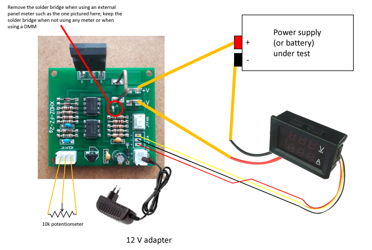
No, that will be fine, because the ground of the DC load is not brought out to J2 (which is the connector made on purpose for an external meter); only the  +0.7 V rail, the anode of D3 if you will, is present there. So the panel meter is powered by 12V minus 0.7V, which is fine.

As a picture is often better than many words, maybe this will help other newbies like me in the future:


Quote
Here is an example: (video)
thank you for the link though, will save it for later, that may very well be useful for another hobby project.

I spent some time studying the circuit in more detail and playing with this little board at my bench.

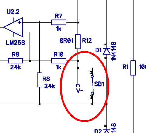
One of the questions I had in my previous posts was, why is it so important that this connection is made ? Given that we have a differential amplifier, why couldn't we let (V-) float?


well, I did a bit of homework and this is what I found :
- the current input between (V+) and (V-) will not be truly floating anyways, because of R1 and R2. So when SB1/J5 is left disconnected, there is current flowing from the +0.7 V rail (D3 anode), through R8 and R7 (not desirable), thus increasing the current through R12, which in turn causes measurement errors because the current in the FET is not anymore equal to the current in R12.
- tying (V-) to the +0.7V rail also ensures that the voltage seen by U2.2 stays within the allowed limits


Also, thanks to your help, here are my other conclusions:
- the LM393 is here as you said to ensure that the FET remains off when nothing is connected, preventing current surges,
- contrary to what I was suggesting before, it's not possible to remove D3 and C4 to get rid of the +0.7V rail and to tie the inverting input of the LM393 to ground, because then there is no way its non-inverting input could go below ground, so the comparator never switches and the FET stays on at startup.
- I think D2 is there to clamp the voltage seen at the (+) input of U1 to 0.7V more than its (-) input, even when the load is connected to a fairly high voltage source (the ebay listings claim up to 100V, not sure I would dare though)
- it is necessary to remove the solder bridge J5 (SB1 on my schematic) when using an external meter as pictured, because otherwise the internal current shunt of the panel meter is short-circuited by the solder bridge, which causes huge measurement errors.

does that make sense?

Also, does anyone have a clue about what D1 is doing ?
For fun I tortured the load with various combinations of reverse voltages on its inputs (with the current limit of my PSU set very low), and I had a 1R resistor in series with D1 to see if it was passing any current, but I haven't found any situation that would make it conduct.

Thank you everyone and please feel free to comment,
JF
 
The following users thanked this post: cichy45

Online MarkF

  • Super Contributor
  • ***
  • Posts: 2548
  • Country: us
Re: understanding this DC load circuit
« Reply #5 on: March 13, 2020, 06:00:39 pm »
I believe diode D1 is to prevent the gate voltage (VGS) from going negative.
 

Offline wagnerlip

  • Newbie
  • Posts: 6
  • Country: us
Re: understanding this DC load circuit
« Reply #6 on: June 26, 2021, 11:50:06 pm »
Old post, but readers don't look post dates, they seek information, even if old.

D1 is a zener diode to protect the gate for excessive voltage (VGS), it can be generated by mistake or by some capacitive discharge through CDG (internal capacitor Drain-Gate).  So, D1 is not a 1N4148, it can be a zener anything from 12 to 15V. 

If your board has in fact a 1N4148 replace with a zener 1N5245 (15V 500mW) or other.

Also, the gate resistor on the drawing, 1kΩ is wrong, too high, replace with a 10~22Ω 1/4W.

The function of D2 is to avoid the MosFET to turn on when powering the unit, or the 258 trying to turn on the MosFET fully when V+ is zero, it will be dangerous to apply V+ with the MosFET gate fully open. It works like a fast time delay in conjunction with C4.  Diode D3 provides a full 0.7Vdc when the power (12V) is flowing through the circuit, but only after C4 fully charges.  This happens pretty quickly, then the inverting input of the 393 will have +0.7V in reference to GND.   If the V+ (external voltage) is turned off, then the division 100k+100k (R1+R2) will provide zeroV in reference to GND to the non-inverting pin of the 393.  This, positive on inverting pin, commands the 393 to short its output, shorting the input of the 258, the same as if you turn the potentiometer fully off, disabling completely the MosFET.   This condition stays the same until the V+ goes above +1.5V, when the 393 reverts and becomes open collector at its output, releasing the 258 to control the MosFET.   D2 can be any kind of diode, even 1N4148, it is to limit the non-inverting input of the 393 voltage to D2+D3 forward vdrop relative to GND.  As the V+ can reach high voltages, around 100V, we don't want half of it (50V) on the non-inverting pin of the 393, so limiting to something less than 10V is a must.

It is a shame not to use the other half of the 393 to verify if the VCC is really above 11V, and if lower, shunt the 258 input to avoid the circuit to run crazy.  It would be really easy to do that, using three resistors and one 1N4148, one resistor promoting current from VCC to the 1N4148 and this voltage ~0.5V to the negative input of the 393, the other two resistors (lets say 100k and 4k3) dividing VCC to produce ~0.5V to the non-inverting input. The 393 output will be open collector only when VCC is in fact above 11V, if lower, the 393 will lock the 258 non-inverting input as zero, protecting everything.   Obviously you can do it easy in the board, just need to remove the 393, cut the traces and install the components.  You can adjust the 4k3 to 4k1 or 4k7 just to make sure it works nicely with 12V, it will depend on the VforwardDrop of the 1N4148 being used.
« Last Edit: June 26, 2021, 11:51:59 pm by wagnerlip »
 
The following users thanked this post: JeanF, ledtester

Offline JeanFTopic starter

  • Regular Contributor
  • *
  • Posts: 142
  • Country: fr
Re: understanding this DC load circuit
« Reply #7 on: July 01, 2021, 03:48:58 pm »
Hello wagnerlip,

thank you very much for your reply.

Your comments complement nicely the previous responses from MarkF; no more mysteries in this circuit!

As you say, this thread is a bit old. Out of curiosity, may I ask how is it that you found it in "the depth" of the forum and decided to reply? Have you been playing around recently with one of these DC loads? :)


Offline wagnerlip

  • Newbie
  • Posts: 6
  • Country: us
Re: understanding this DC load circuit
« Reply #8 on: August 02, 2021, 02:13:04 am »
Hi JeanF, yes, I work for many years with all kinds of power supplies, mostly industrial ones, and always designing/building electronic load for testing those beasts, some reach kilowatt or more.   I am always looking around to see what people create different, but nothing different was found, it is always the same.  What I made in my circuits is just small protection to avoid problems, just making sure the EL starts with the MosFET off, gradually increasing current to the setup (100ms or around it), also measuring power dissipated and anticipating any trouble on the MosFET.   For some reason I hit this post, and as I always do, no matter how old the posts, any new hint or tip will always help somebody else looking for the same thing.  I am one of the creator of an old electronic forum, more than 16 years old, with thousand of users, and I use to help all requests.  Working with digital/analog electronics for more than 50 years, I always believe knowledge only makes sense if it is forwarded to others.  Cheers, Wagner.
 
The following users thanked this post: xrunner, Ian.M, ledtester

Offline ledtester

  • Super Contributor
  • ***
  • Posts: 3036
  • Country: us
Re: understanding this DC load circuit
« Reply #9 on: August 02, 2021, 11:59:00 pm »

PS : EEVBlog user ledtester posted about it a while back but I thought it was better to post a new thread, for clarity. I hope it's OK!


Working link to that thread:

https://www.eevblog.com/forum/beginners/xhdz-fz-2g-electronic-load-comparator-function/msg1523191/#msg1523191

About the wiring of the control pot...

I recall that I couldn't set the current down to 0, but if I moved the lower leg of the pot to GND instead of the 0.7V rail then I could go to 0 although there was a large dead space at the lower end of the pot.

Does that sound right?


Share me

Digg  Facebook  SlashDot  Delicious  Technorati  Twitter  Google  Yahoo
Smf