The security system.
The PIF inside the N64 contains a small 2kb IPL that the R4300 cpu boots at power-on reset. This is mapped to the cpu's reset vector via the RCP.
However, the PIF will not load the next IPL until it talks to the security chip that is in each cartridge.
I have both chips decapped and I will try to get them posted up here soon.
PIF is actually a Sharp custom labeled part. It is their own SM5 4-bit microcontroller. You take the core and slap on whatever IO you need. In this case it has 1kbyte mask rom internaly (in addition to the IPL). My theory is that all the controller polling (using a manchester encoded 1wire signal) and serial comms with the RCP glue logic is done by the huge amount of cell logic on the chip. It is like a cheap ASIC.
In the cartridges is where the CIC lives. It is also the exact same SM5 core, 1k rom with 32 nybbles of RAM.
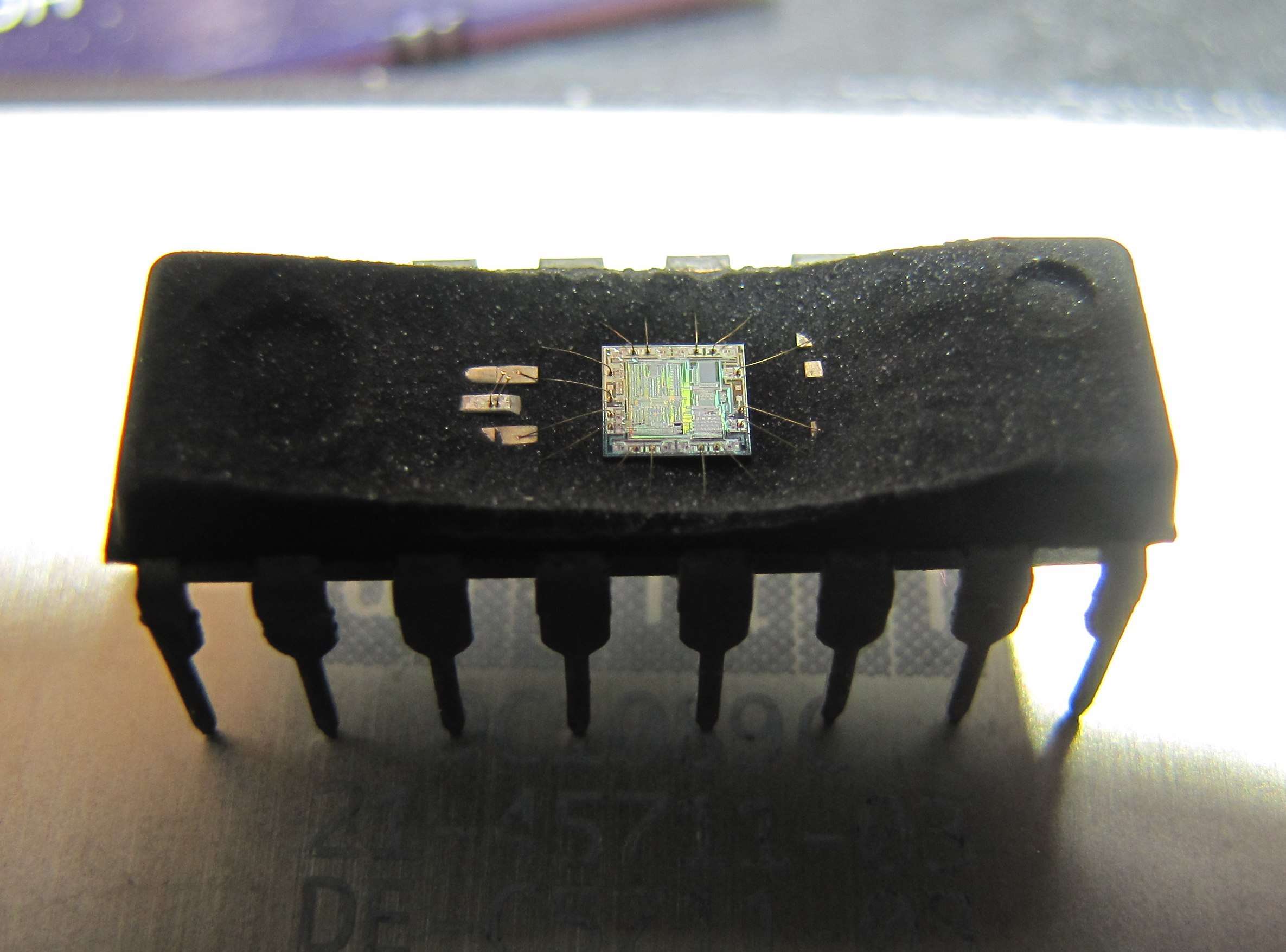
Full die image:
http://retroactive.be/cic/cic_20x_die_image.jpg (Credit - Dr decap)
Using a SPI-like interface they constantly talk to each other while turned on, after exchanging the following info that is cooked into each CIC's mask ROM (there were about 14 variations):
- Region code (NTSC / PAL)
- "Lockout code", 5 different types
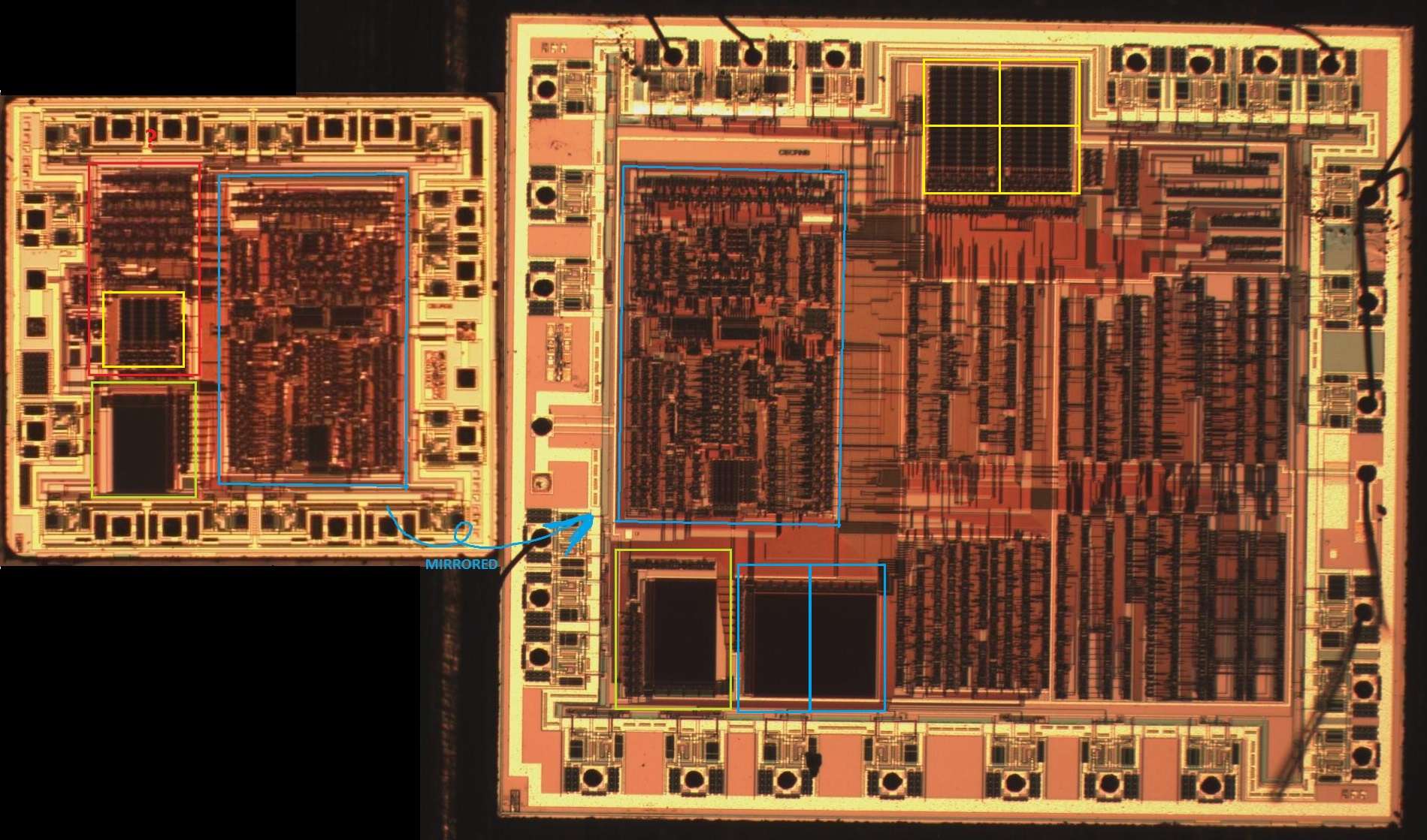
Here are the PIF and CIC dies side by side. You can see the identical SM5 cores in both (they are mirrored) sans IO in the PIF. And the right area is all the cell logic.
Bottom left are the SM5's own mask rom (yellow) and the MIPS cpu's IPL (blue)
Photo credits: Anonymous friend