Author Topic: The most awful/ugly PCB thread.  (Read 10714 times)

0 Members and 1 Guest are viewing this topic.

Offline RefrigeratorTopic starter

  • Super Contributor
  • ***
  • Posts: 1541
  • Country: lt
The most awful/ugly PCB thread.
« on: March 10, 2014, 09:22:28 pm »
Share your pics of the most ugly PCBs you have ever seen.
PCBs that don't deserve anything but get thrown away.
I don't have any right now since they're where they belong - in the trash.
I have a blog at http://brimmingideas.blogspot.com/ . Now less empty than ever before !
An expert of making MOSFETs explode.
 

Offline dexters_lab

  • Supporter
  • ****
  • Posts: 1890
  • Country: gb
Re: The most awful/ugly PCB thread.
« Reply #1 on: March 11, 2014, 10:30:49 am »
this was the first PCB i ever made myself, I'd only ever used stripboard before.

Was a big learning curve, i didn't have a clue about anything... after scratching my head looking at eagle for hours i think i just placed a few components in roughly where i wanted them, the others got thrown anywhere else and then i just hit the autoroute button  :-[ Some random place in china made them, but they did work!

I learned a massive amount from the exercise though and was well worth the time and money

hopefully there is worse out there :-DD


Offline poorchava

  • Super Contributor
  • ***
  • Posts: 1672
  • Country: pl
  • Troll Cave Electronics!
Re: The most awful/ugly PCB thread.
« Reply #2 on: March 11, 2014, 12:29:18 pm »
I'm pretty sure there has already been a thread like this before...
I love the smell of FR4 in the morning!
 

Offline Richard Head

  • Frequent Contributor
  • **
  • Posts: 685
  • Country: 00
Re: The most awful/ugly PCB thread.
« Reply #3 on: March 11, 2014, 12:36:43 pm »
If that's the first PC board you have ever laid out I would say you are doing extremely well. :-+
I regularly do layouts and never get it perfect first time, even with all the tools such as DRC etc.
There's always some damn hole that's too small or some other issue.
I have just accepted that the PC boards takes a couple of iterations to get perfect.

Dick
 

Offline tszaboo

  • Super Contributor
  • ***
  • Posts: 7369
  • Country: nl
  • Current job: ATEX product design
Re: The most awful/ugly PCB thread.
« Reply #4 on: March 11, 2014, 10:26:22 pm »
I had a board, patched, where an awesome university student autorouted all NC pins together across several digital ICs and stuff. On four layer. Had about a million via.
 

Offline zapta

  • Super Contributor
  • ***
  • Posts: 6190
  • Country: us
Re: The most awful/ugly PCB thread.
« Reply #5 on: March 11, 2014, 10:35:19 pm »
The PCB does not look awful at all. 

BTW, you may find this useful http://www.alternatezone.com/electronics/files/PCBDesignTutorialRevA.pdf ,
 

Offline steve30

  • Frequent Contributor
  • **
  • Posts: 733
  • Country: england
    • Stephen Coates' Homepage
Re: The most awful/ugly PCB thread.
« Reply #6 on: March 12, 2014, 05:59:53 am »
dexters_lab: I think that board looks quite nice. I guess if you were being fussy, the track layout could probably be better, but I've definitely seen a lot worse.

I reckon suitable candidates for this thread would be those ultra cheap chinese consumer type products.
 

Offline Skimask

  • Super Contributor
  • ***
  • Posts: 1433
  • Country: us
Re: The most awful/ugly PCB thread.
« Reply #7 on: March 12, 2014, 07:24:14 am »
My latest creation.  Threw it together for prototyping.  Auto-routed it in EAGLE! :)  Spent a couple days re-routing everything, getting rid of via's, straightening tracks, etc.  Got the via count down to something like 140 or so....down from over 600.
Haven't populated it yet.  Still working on the reflow oven.
For scale, the PCB is 6.0" x 3.4"
« Last Edit: March 12, 2014, 07:30:50 am by Skimask »
I didn't take it apart.
I turned it on.

The only stupid question is, well, most of them...

Save a fuse...Blow an electrician.
 

Offline DeanA

  • Regular Contributor
  • *
  • Posts: 115
  • Country: au
    • Design Electronics
Re: The most awful/ugly PCB thread.
« Reply #8 on: March 12, 2014, 09:56:51 am »
Hi Skimask,
I had a quick look at your board layout and it looks good, my only comment would be "where is the ground?"  Without seeing the circuit I assumed that some of the grounds were the negative side of your electros, but they're all connected by the same width tracks as your signal tracks.  You might want to consider getting some kind of ground plane, I normally use the opposite side to the SMT as my ground layer side for double sided boards, only routing signal tracks on that layer if unavoidable.  At the very least I would look at thickening up the ground tracks and your power tracks to reduce impedance.
Regards,
Dean.

Offline uwezi

  • Supporter
  • ****
  • Posts: 272
  • Country: se
    • GreenPhotons
Re: The most awful/ugly PCB thread.
« Reply #9 on: March 12, 2014, 10:48:57 am »
Hi Skimask,
I had a quick look at your board layout and it looks good, my only comment would be "where is the ground?" 

From the number of uncommitted vias all around the board I guess there are more than 2 layers involved, but the traces to the SMD electrolytics and bypassing caps seem a bit on the narrow side.
 

Offline uwezi

  • Supporter
  • ****
  • Posts: 272
  • Country: se
    • GreenPhotons
Re: The most awful/ugly PCB thread.
« Reply #10 on: March 12, 2014, 10:50:44 am »
this was the first PCB i ever made myself, I'd only ever used stripboard before.
...

hopefully there is worse out there :-DD

Your board does not qualify under this topic! Definitely not!
 

Offline DeanA

  • Regular Contributor
  • *
  • Posts: 115
  • Country: au
    • Design Electronics
Re: The most awful/ugly PCB thread.
« Reply #11 on: March 12, 2014, 11:08:32 am »
Hi Skimask,
I had a quick look at your board layout and it looks good, my only comment would be "where is the ground?" 

From the number of uncommitted vias all around the board I guess there are more than 2 layers involved, but the traces to the SMD electrolytics and bypassing caps seem a bit on the narrow side.

Ahh, is that what all those square pads are? Vias onto an internal ground layer. Like a man wearing orthopedic shoes, I stand corrected. ;D  I missed it because those ground/power nets still seemed to be routed on the signal layers and in some cases there is some distance in thin tracks before they connect to the internal layer through the square via.
 

Offline Joule Thief

  • Regular Contributor
  • *
  • Posts: 249
  • Country: us
Re: The most awful/ugly PCB thread.
« Reply #12 on: March 12, 2014, 11:08:49 am »
But it does make one wonder if performance should ever be sacrificed for "looks".

She might be ugly but she sure can cook !! ;D
Perturb and observe.
 

Offline uwezi

  • Supporter
  • ****
  • Posts: 272
  • Country: se
    • GreenPhotons
Re: The most awful/ugly PCB thread.
« Reply #13 on: March 12, 2014, 11:53:51 am »
From the number of uncommitted vias all around the board I guess there are more than 2 layers involved, but the traces to the SMD electrolytics and bypassing caps seem a bit on the narrow side.

Ahh, is that what all those square pads are? Vias onto an internal ground layer. Like a man wearing orthopedic shoes, I stand corrected. ;D  I missed it because those ground/power nets still seemed to be routed on the signal layers and in some cases there is some distance in thin tracks before they connect to the internal layer through the square via.

...and I just had yet another look. The dashed line all around indicates an (invisible) copper pour on at least one side of the board. Eagle usually hides those until you make a new "ratsnest" update. But I guess Skimask would have to fill in the details.

And I fully agree on your diagnosis of the thin power tracks
 

Offline HP-ILnerd

  • Frequent Contributor
  • **
  • Posts: 259
  • Country: us
Re: The most awful/ugly PCB thread.
« Reply #14 on: March 12, 2014, 12:32:37 pm »
Come on!  You guys are hardly trying!   ^-^
Here's the "eyes" of a robot I built for a convention that was done on a Thursday night with the convention starting Saturday morning.  The rush was mostly just a case of running out of time.
PCB cut with a dremel, traces drawn with a sharpie.  You'll notice there are no resistors for the red pins on the RGB LEDS because it turned out red wasn't one of the colors being used.  The ground line is across the top.


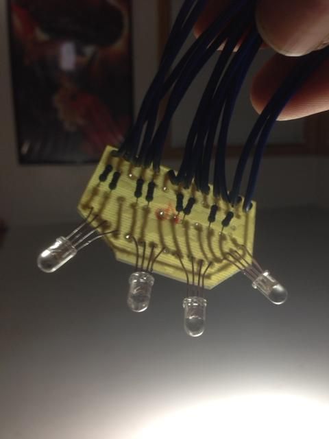
The whole thing is driven by an Arduino Lilypad (I was happy to find a use for the little guy).   The Lilypad doesn't actually have enough PWM outs to drive this, so I had to "manually" PWM the LED pins in software via the regular outs.   This actually worked out really well, and while the hardware may not be pretty, I'm happy with the software.  Two adjacent LEDS are on at a given time so it can "look" left, right, forward and squint by dimming to a different darker color.  There is an extensive script to make the pattern seem natural.

When I get some spare time (right) I should be able to get the whole thing down to a single board, LEDS, power supply, charger and MCU.
Until then, I'm living with it.  It works great.
 

Offline uwezi

  • Supporter
  • ****
  • Posts: 272
  • Country: se
    • GreenPhotons
Re: The most awful/ugly PCB thread.
« Reply #15 on: March 12, 2014, 01:04:15 pm »
Come on!  You guys are hardly trying!   ^-^

PCB cut with a dremel, traces drawn with a sharpie.

There is nothing wrong with hand-drawn circuit boards. I keep this one to show to my students:
 

Offline SeanB

  • Super Contributor
  • ***
  • Posts: 16276
  • Country: za
Re: The most awful/ugly PCB thread.
« Reply #16 on: March 12, 2014, 06:39:19 pm »
I would show some I made in the early 1980's, hand drawn, but they are buried inside a machine and I really do not want to dig that far down inside to get to them. I did make a big mistake with the one and mirrored it, so wired it up with components on the solder side and left it at that. Would not have been a problem except there were a few DIP packages there and turning the pins around would have looked funny. Looks crappy but still works.
 

Offline liquibyte

  • Frequent Contributor
  • **
  • Posts: 475
  • Country: us
Re: The most awful/ugly PCB thread.
« Reply #17 on: March 12, 2014, 07:10:48 pm »
Well, since it's not working right and I thought it should be and is consistently wrong on both outputs, my latest fiasco on some RS pad per hole board....  I wish I had the capability to do etching but to date have never done one. 
 

Offline dexters_lab

  • Supporter
  • ****
  • Posts: 1890
  • Country: gb
Re: The most awful/ugly PCB thread.
« Reply #18 on: March 12, 2014, 07:25:07 pm »
dexters_lab: I think that board looks quite nice. I guess if you were being fussy, the track layout could probably be better, but I've definitely seen a lot worse.

I reckon suitable candidates for this thread would be those ultra cheap chinese consumer type products.

lol yea, after that first attempt i realised how important location and rotation was!

i am sure there should be some far-eastern horrors to be seen

Offline electronics man

  • Frequent Contributor
  • **
  • Posts: 686
  • Country: gb
Re: The most awful/ugly PCB thread.
« Reply #19 on: March 12, 2014, 07:35:25 pm »
Well, since it's not working right and I thought it should be and is consistently wrong on both outputs, my latest fiasco on some RS pad per hole board....  I wish I had the capability to do etching but to date have never done one.

For perfect board that. Pcb is very neat
follow me on twitter @get_your_byte
 

Offline bronson

  • Regular Contributor
  • *
  • Posts: 172
  • Country: us
Re: The most awful/ugly PCB thread.
« Reply #20 on: March 12, 2014, 08:43:40 pm »
Ain't nothing wrong with a a nice gridded perfboard layout.

Well, other than requiring $5.00 of solder to bridge everything together.
 

Offline tom66

  • Super Contributor
  • ***
  • Posts: 6697
  • Country: gb
  • Electronics Hobbyist & FPGA/Embedded Systems EE
Re: The most awful/ugly PCB thread.
« Reply #21 on: March 12, 2014, 09:11:48 pm »
One of the students in my lab class apparently produced this for a motor controller.

Just... no.

I've been told that the suggested method of routing is to route left one layer, and down on the other.  That's one sure way to produce an ugly, poorly optimised layout.
 

Offline liquibyte

  • Frequent Contributor
  • **
  • Posts: 475
  • Country: us
Re: The most awful/ugly PCB thread.
« Reply #22 on: March 12, 2014, 09:35:35 pm »
Ain't nothing wrong with a a nice gridded perfboard layout.

Well, other than requiring $5.00 of solder to bridge everything together.

Except for the fact that it's supposed to be outputting 30V and is only getting up to between 9 and 10V I'd say it looks nice but doesn't do what it's designed to do.  I'm thinking I may just have boards made and start over.
 

Offline Skimask

  • Super Contributor
  • ***
  • Posts: 1433
  • Country: us
Re: The most awful/ugly PCB thread.
« Reply #23 on: March 12, 2014, 11:45:19 pm »
From the number of uncommitted vias all around the board I guess there are more than 2 layers involved, but the traces to the SMD electrolytics and bypassing caps seem a bit on the narrow side.
Ahh, is that what all those square pads are? Vias onto an internal ground layer. Like a man wearing orthopedic shoes, I stand corrected. ;D  I missed it because those ground/power nets still seemed to be routed on the signal layers and in some cases there is some distance in thin tracks before they connect to the internal layer through the square via.
...and I just had yet another look. The dashed line all around indicates an (invisible) copper pour on at least one side of the board. Eagle usually hides those until you make a new "ratsnest" update. But I guess Skimask would have to fill in the details.
And I fully agree on your diagnosis of the thin power tracks

Yes...woefully thin power tracks.  That's one of the after-thoughts I had.  On the upside, at most, I'll be pulling 1 amp from the 12v rails (ATX power connector on the right).  If I come up short (eg. too much resistance), guess I'll end up adding some hard wire bodges to try and help out those thin traces.

Uncommitted vias - rough attempt at some top-to-bottom ground plane stitching.  On the top and bottom, basically anything that's not covered by traces is a ground, unless it's a 'ground island', then no connection.  I tried to make every part of the board that wasn't otherwise being used a ground.  Don't know if that's the right method, but it seemed right to me.

Next rev of the board - more, thicker power runs everywhere, and I'll be ditching the ATX power supply connector on the right for a single 3 cell LiPo pack input, and various boost and buck regulators giving me all the + and - voltages I need, not to mention adding a few inductors in there to help out with smoothing the power.

For the first run, using an ATX PSU was dirt cheap and quick, even if it will be a bit noisy.
I didn't take it apart.
I turned it on.

The only stupid question is, well, most of them...

Save a fuse...Blow an electrician.


Share me

Digg  Facebook  SlashDot  Delicious  Technorati  Twitter  Google  Yahoo
Smf