I am running this old prog under a winXP VM. It works great and I have done many many designs with it. I am also more than familiar with its cryptic and mostly useless DRC errors, which in most cases are solved by trial and error only; the .drc file is almost useless.
But now I have a weird problem and wonder if somebody of sufficient age might remember how to deal with it. I have this PCB with a split ground plane (Internal Plane 1):
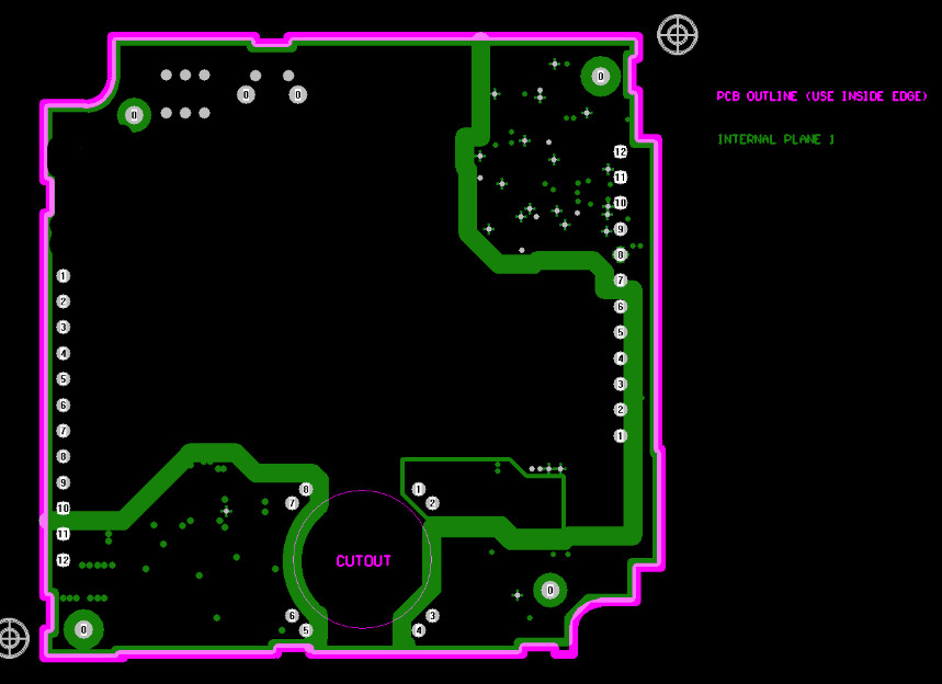
Placing pads in each these four areas, with all the pads having a "relief to Plane 1" should not produce a conflict. The nets are GND1 GND2 GND3 GND4. But Protel is in some cases joining them up - as if the planes were joined. I have carefully checked that the tracks placed on the Plane 1 layer have no breaks in them, since that would be an obvious cause. The way to generate split planes is to place a track on the plane layer. I wondered if one is supposed to use a Polygon Plane? I tried that and it doesn't seem to make any difference.
There are cases where one has to just give up and accept some DRC errors but I don't like doing it. Usually, by clicking on some random track, the DRC error goes away, but I have spent a few days on this and can't solve it.
The DRC errors are listed as broken subnets, but clearly they are physically connected within each piece of the plane. However listing broken subnets when actually there is some clearance error or a short, has always been a feature of Protel PCB...
I also wonder if anyone knows what the coordinates in the DRC error listing mean? They are not within the PCB area...
Clearance Error
Track (1138mil,2581mil 1268mil,2581mil) Top Layer +DCIN
Pad (1138mil,2583.047mil) Multi-Layer No Net
Clearance Error
Track (3293mil,2681mil 3293mil,2741mil) Top Layer GND_2
Pad (3293mil,2743mil) Top Layer GND_1
Clearance Error
Track (3388mil,2186mil 3388mil,2281mil) Top Layer -20V_2
Pad (3388mil,2286mil) Top Layer No Net
Many thanks for any tips.


