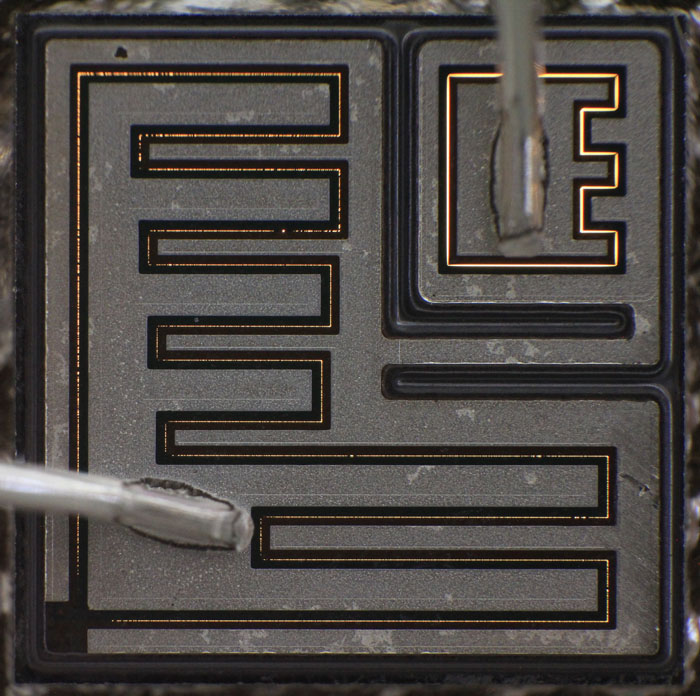
Some more pictures of the Motorola MJ3001:
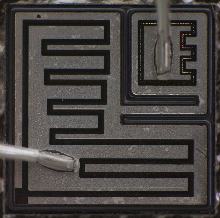
Yeah, base emitter breakdown!

The driver transistor is glowing first because at lower currents (0,03A) the base emitter resistor of the power transistor (50

) doesn´t provide enough voltage to drive the base emitter junction of the power transistor into avalanche breakdown.
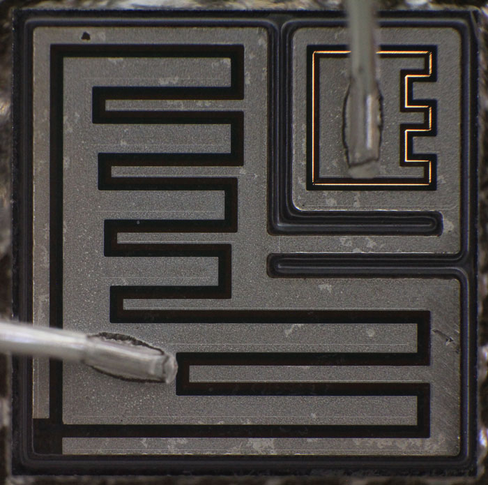
0,2A
At 0,5A there is a first light in the power transistor. Can you locate it?

Here we have a voltage drop of 26V. Assuming the voltage across the driver transistor is still around 13V the voltage drop across the power transistor is 13V too. It´s plausible that both have the same breakdown voltage. To get 13V with a current of 0,5A the resistor across the base emitter junction has to be around 26
(datasheet says 50
).
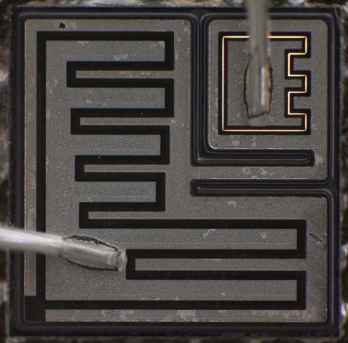
With a voltage drop of 10V across the whole MJ3001 you can estimate a base emitter resistance across the driver transistor of 7k
(datasheet says 2k
).
Well the exact resistances aren´t important and resistors in semiconductors often own a high tolerance.
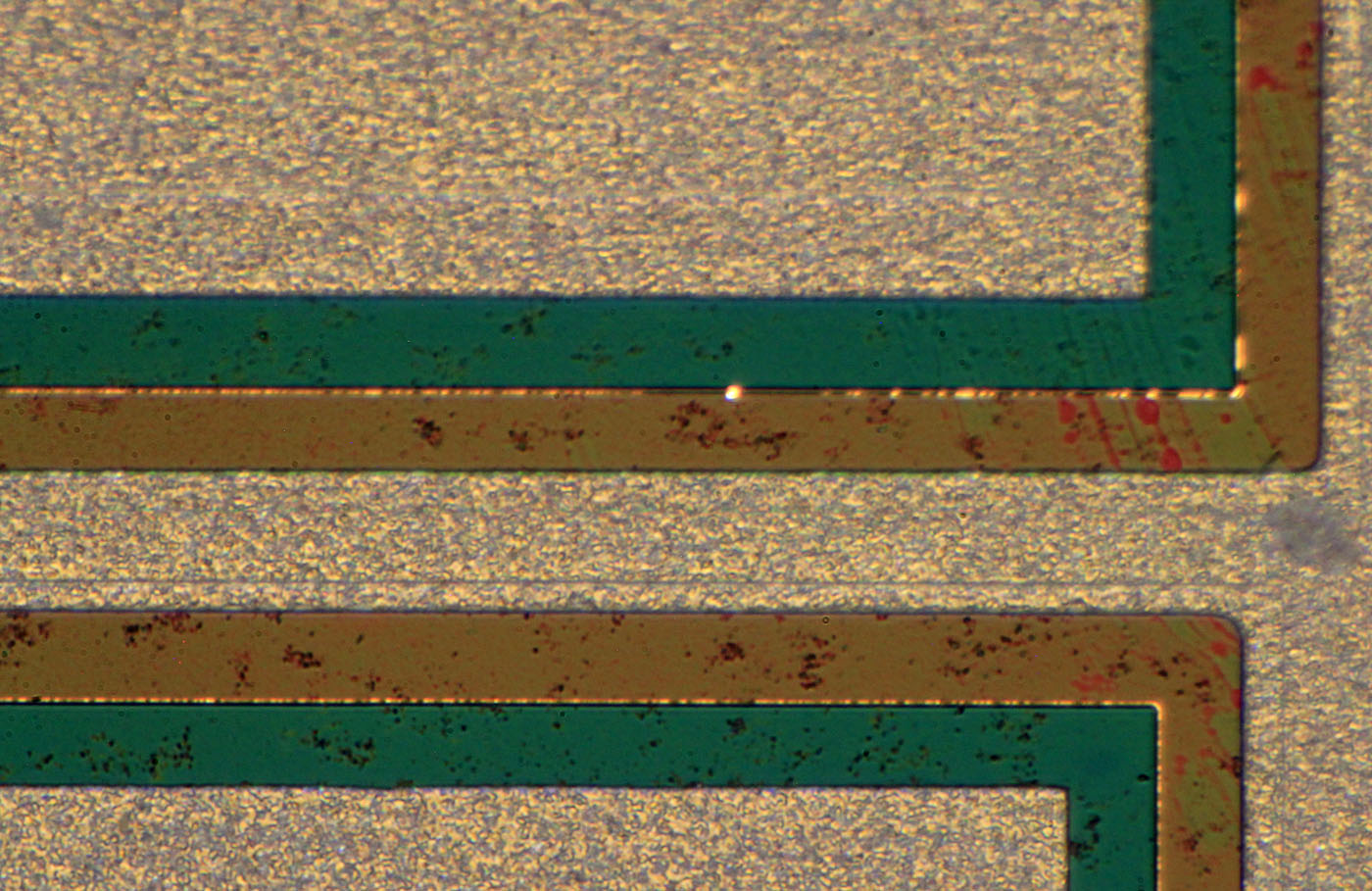
0,6A, there are quite some "highlights" and darker areas.
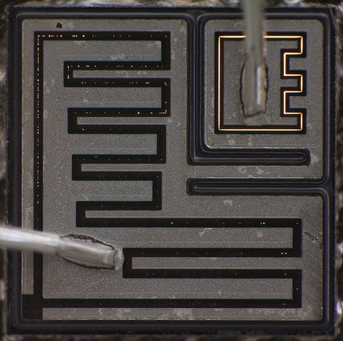
0,9A, still the light is not very uniform.
Through the base emitter resistor of the power transistor there has to flow a current of 0,5A. For the base emitter junction there are only 0,4A left. 0,4A over a larger area gives a dimmer light than 0,9A through the smaller area of the driver transistor.
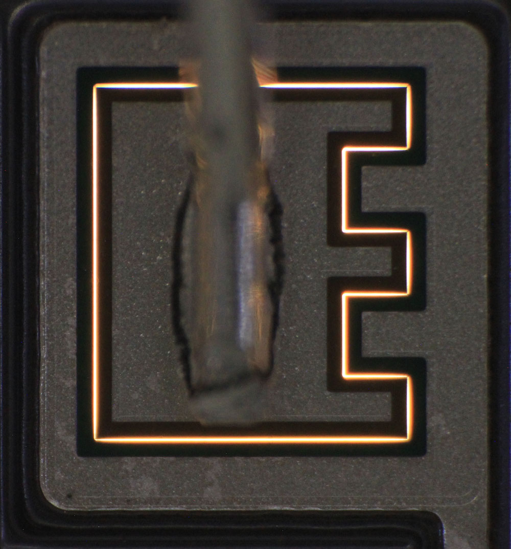
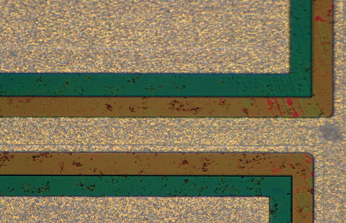
That´s interesting: The light in the driver transistor is quite wide.
You can see it´s no focus problem because in the corners there are sharp structures.
The light extends wider into the inner base area than into the outer emitter area. Perhaps that is due to the doping concentrations? The higher doped emitter occupies less of the junction than the lower doped base.
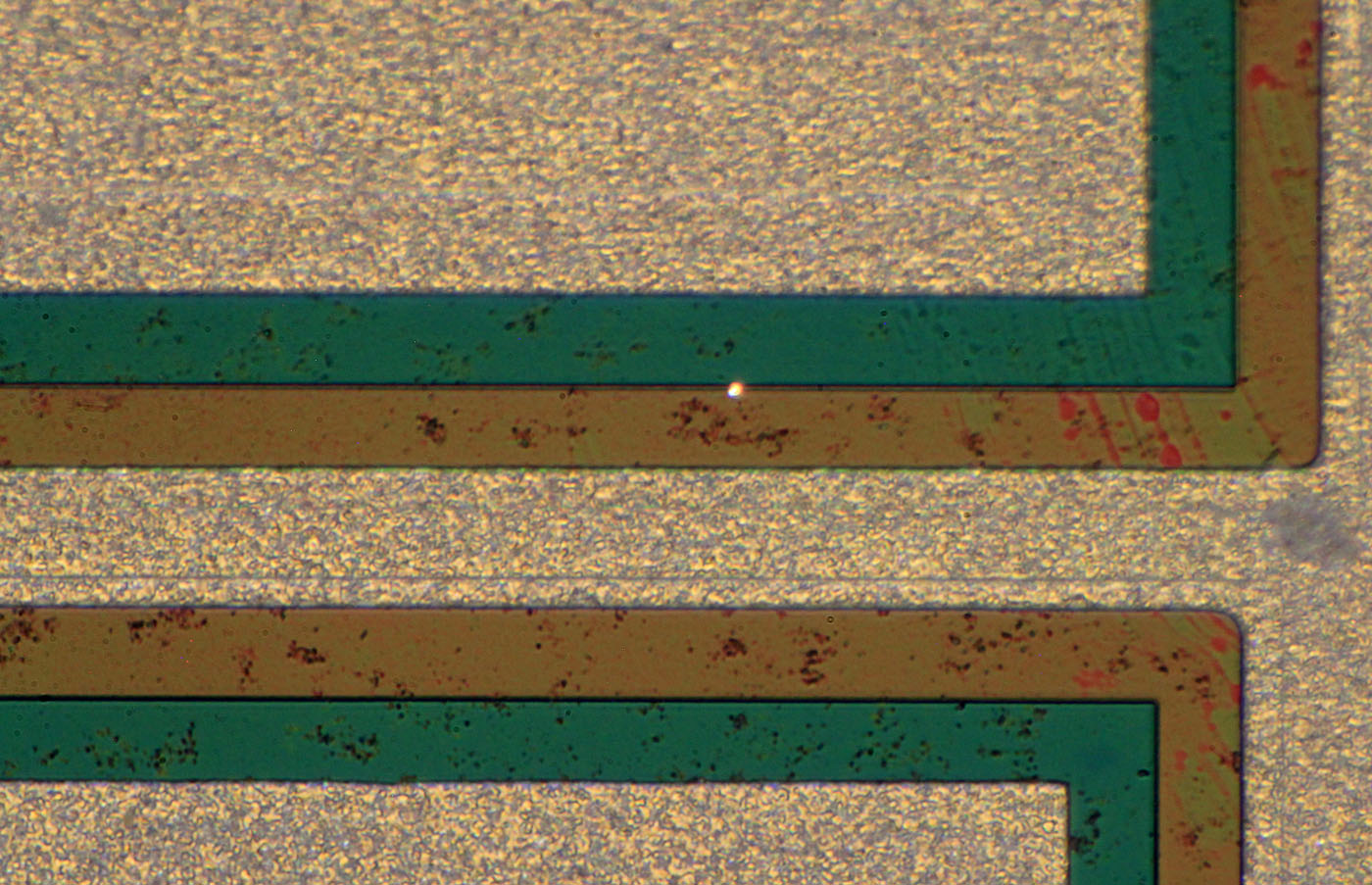
Here we see the small defect that shows first light and consumes current from the nearby areas that stay dark at higher currents.
We have seen a similar defect / effect in one of the BUX22:
https://www.richis-lab.de/Bipolar07.htm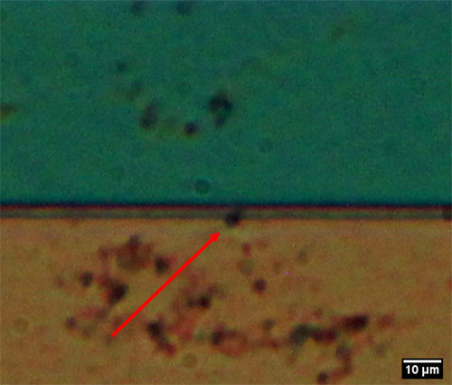
The defect is a point with a diameter of round about 4µm.
Some more pictures here:
https://www.richis-lab.de/Bipolar64.htm 


