Unfortunately you don't get to make that trade-off as instruction decode and control takes a large proportion of the area of a CPU, and doesn't vary much depending on whether the registers and ALU are 8, 16, 32 or 64 bits. For example, the decode and control on a 64 bit RISC-V Rocket core is just about identical to that on a 32 bit RISC-V Rocket core.
So, it's more likely that you'd actually get to choose between one 1-GHz 32-bit CPU, or two or maybe three 1-GHz 8-bit CPUs.
Most of the control that you're referring to is not required in light-weight cores:
- There's no pipeline, so no need for pipeline control.
- There's no cache, so there's no need for cache and big memory controllers.
- We won't worry about code density (because the performance doesn't depend
on decoding speed), so we can have really long instructions, such as 32-bit.
This way the instruction will come out already decoded to a great extent
- We'll also get rid of the bus with all the bus arbitrage and collisions, and
let our small cores communicate through dedicated FIFOs.
That turns out not to be the case. On simple processors the control is the majority of the chip.
For example here's a labelled photo of a Z80
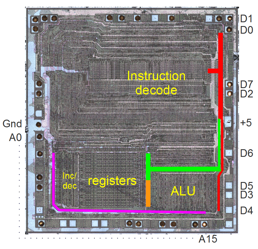
You'll observe that the control logic is something like 60% of the chip, and the registers and ALU 40% (to be generous).
If you made a chip with the same instruction set with the same encoding, but just made the registers and ALU two or four times wider, the control part would stay the same size while the registers and ALU would get bigger, roughly in proportion to the bit width. So the control part would get relatively smaller. So a 32 bit Z80 might be 25% control and 75% registers and ALU.
In the end, it'll be much less of silicon for each core. May be not 16, but close. More importantly, you
may be able to run the whole thing faster and will end up with 2 GHz 8-bit cores, or even 3 GHz 8-bit
cores. This would certainly beat the current behemoths.
There is no reason for a 2x or 4x wider data path to run 50% more slowly. The only place it will make any difference at all is carry propagation in adders, but that's logarithmic if done correctly. Basically, a 32 bit adder has two gates more delay than an 8 bit adder. And the adder isn't usually the clock-limiting factor anyway.
You either pipeline it, then each stage requires its own multiplier, or you don't, in which case next multiply commands will be sitting there waiting for its turn.
Multiplies are rare. Two multiplies in a row are *very* rare.
The Coremark and Dhrystone benchmarks, for example are quite heavily influenced by multiply performance.
I just checked on my HiFive1 "Arduino" board (32 bit RISC-V "Rocket" microcontroller running at 256 MHz). It has a 4 cycle multiplier which allows following instructions to continue as long as they are not multiplies (or divides) and as long as they do not need the result of the multiply. I used gcc 7.2.0.
Coremark/MHz with hardware multiply: 2.68
Coremark/MHz with software multiply: 0.94
Dhrystone/MHz with hardware multiply: 1.56
Dhrystone/MHz with software multiply: 0.85
For comparison, for the Cortex M3/M4 ARM claims
http://www.eeherald.com/section/design-guide/arm_cortex_m3_m4_mcu.html 2.17 Coremark/MHz and 1.25 Dhrystone/MHz.
ARM manuals say the M3/M4 has a single-cycle multiplier. But it's coming out considerably slower than the chip with the 4 cycle multiplier on benchmarks where multiplication is important (as seen by software emulation being much slower)
As in most real-case uses of multiply, Coremark (for example) is generally loading two values from memory, then multiplying them, then storing the result, and then looping. There are plenty of other instructions around the multiply that a four cycle latency is no big deal.


