Author Topic: PLL design with ADF4001 does not work  (Read 3950 times)

0 Members and 1 Guest are viewing this topic.

Offline YrrahTopic starter

  • Contributor
  • Posts: 25
  • Country: nl
PLL design with ADF4001 does not work
« on: October 28, 2021, 08:07:19 am »
Hello,

I am trying to design a simple PLL controlled 100 MHz VCXO disciplined by a 10 MHz reference. The purpose is stabilize the 100 MHz oscillator while maintaining its good PN characteristics. I use a ADF4001 PLL chip in agreement with the datasheet, its registers are loaded with an Arduino. The ADF is fed by the Arduino 5V pin (for testing). I use the "Counter Reset Method", per datasheet. So far I have not even come to close the loop. I can load the registers with the proper counter data. Both input signals (100 MHz and 10 MHz via attenuators) are counted down to 25 kHz, the pfd frequency. They show up at the MUX output as needle pulses every 40 usec. I see some activity at the CP terminal with a scope via a 1kohm resistor. Then after a while the CP output keeps quiet and the N counter seems dead. The R counter works. I can not get out of this situation. I have made two testboards with the same results. Power up/down and reloading registers does not help. Is this a hw failure, a lock-in of the PLL chip or what? Before making a third board I'd like to know what to change....
Any help appreciated,
Harke, PA0HRK
 

Offline KE5FX

  • Super Contributor
  • ***
  • Posts: 1889
  • Country: us
    • KE5FX.COM
Re: PLL design with ADF4001 does not work
« Reply #1 on: October 28, 2021, 08:23:52 am »
Assuming the charge pump polarity is correct, you might be overdriving it, or otherwise getting into a situation where it's trying to lock to a harmonic. 

The ADF4xxx parts are basically copies of the LMX2xxx parts from National Semiconductor, and virtually everything that applies to the LMX series applies equally to the ADF series.  NatSemi published a superb handbook of design info and troubleshooting hints for these PLL chips, known as "Dean's Book."  It's still available from TI, and is highly recommended.  The author is an app engineer who's seen every possible thing that can go wrong with these parts.  Whatever you're doing wrong, rest assured, he covers it.
 
The following users thanked this post: DC1MC, Yrrah

Offline HB9EVI

  • Frequent Contributor
  • **
  • Posts: 722
  • Country: ch
Re: PLL design with ADF4001 does not work
« Reply #2 on: October 28, 2021, 11:47:30 am »
how did you design the loop filter?
 
The following users thanked this post: croma641

Offline YrrahTopic starter

  • Contributor
  • Posts: 25
  • Country: nl
Re: PLL design with ADF4001 does not work
« Reply #3 on: October 29, 2021, 09:52:26 am »
Thanks for the link, John. Excellent reading!.
I managed to make the ADF4001 working again: I programmed all Timeout bits of the Function Latch to one. No clue. I also adjusted the input levels to about 3 dB above garbage. VCXO characteristics: Fnom=100 MHz, EFC: 1 kHz/V. EFC @ 100 MHz: 2.215 V. EFC input cap: 100 nF. Now its time to close the loop. With Vefc = 0V the VCXO frequency is little below 100 MHz. With Fref = 10 MHz the output of the CP is high (=+5V). Loop filter is calculated with ADIsimPLL. C1=31 nF + internal 100 nF. R1 =60.7 K and C2 = 633 nF. For a first test approximations are ok, I think. Loop BW = 10 Hz. Close the loop: CP stays high. Fvcxo is little above 100 MHz. No luck/lock. What else can I think of?
TIA, Harke
 

Offline capt bullshot

  • Super Contributor
  • ***
  • Posts: 3033
  • Country: de
    • Mostly useless stuff, but nice to have: wunderkis.de
Re: PLL design with ADF4001 does not work
« Reply #4 on: October 29, 2021, 11:34:24 am »
I've no idea if this helps, I'll post it anyway:
This is the initialization code I've used for a quite similar purpose ADF4001 circuit (control a 100MHz VCXO from a 10MHz reference).
I don't have the schematic of the loop filter available right at this moment, I might try to find it later today. It's a design made with the ADI PLL design software, I've chosen a higher order for better phase noise, afair about 20kHz BW.
In the first version I had the maximum charge pump current and a rather low PD operating frequency. In this version I'm using a higher PD frequency (yields better
phase noise results), but I had to reduce the charge pump current. With max. current, it was unstable.

Code: [Select]
void adf_out(unsigned long v)
{
int i;
RESET_LE;
RESET_CLK;
for (i=0; i<24; i++) {
if (v & 0x00800000) SET_DATA; else RESET_DATA;
SET_CLK;
asm("nop; nop;");
RESET_CLK;
asm("nop; nop;");
v<<=1;
};
SET_LE;
asm("nop; nop;");
RESET_LE;
RESET_CLK;
RESET_DATA;
}

void init_adf(void)
{
unsigned long ref, n, func;
ref= (1 << 20) | // Lock detect precision
(0 << 18) | // Test mode bits
(1 << 16) | // Anti-Backlash width
(30 << 2) | // Reference counter //400
0x00; // Control bits
n = (0 << 21) | // CP gain
(300 << 8) | // N counter //4000
(0 << 2) | // reserved
0x01; // Control bits
func = (0 << 21) | // PD2
   (0 << 18) | // Current setting 2 /7
   (0 << 15) | // Current setting 1 /7
   (0 << 11) | // Timer counter control
   (0 << 9)  | // Fastlock mode / control
   (0 << 8)  | // CP Three-state
   (1 << 7)  | // Phase detector polarity
   (4 << 4)  | // Muxout control
   (0 << 3)  | // PD1
   (0 << 2)  | // Counter reset
   0x03; // Control bits
adf_out(func);
adf_out(ref);
adf_out(n);
}


« Last Edit: October 29, 2021, 11:37:54 am by capt bullshot »
Safety devices hinder evolution
 

Offline KE5FX

  • Super Contributor
  • ***
  • Posts: 1889
  • Country: us
    • KE5FX.COM
Re: PLL design with ADF4001 does not work
« Reply #5 on: October 29, 2021, 07:24:03 pm »
Something else to watch out for may be the ground returns for your reference and VCO inputs.  Try to keep these signals and their ground returns separate, rather than allowing them to flow in parallel or past one another. 

For instance, don't run the reference from a coax jack on the other side of the VCO circuitry, or vice versa.  I've seen definite, repeatable locking problems under those conditions (for one example, ctrl-f this page for the word 'crosstalk').

Contrary to what I said earlier, I don't believe Dean actually addresses this. :(  He primarily discusses grounding issues in the context of spur optimization, rather than lock failure.  As I recall I had to figure it out for myself.   What I was seeing on the Stellex board didn't make any sense, but changing the physical layout of my external clock input hack fixed the problem 100% of the time.
 

Offline YrrahTopic starter

  • Contributor
  • Posts: 25
  • Country: nl
Re: PLL design with ADF4001 does not work
« Reply #6 on: October 29, 2021, 07:44:29 pm »
I cannot read that code very well. I have a simple Arduino register loading sketch.
John: please refer to the picture attached. Do you expect any problems from this setup?
 

Offline KE5FX

  • Super Contributor
  • ***
  • Posts: 1889
  • Country: us
    • KE5FX.COM
Re: PLL design with ADF4001 does not work
« Reply #7 on: October 30, 2021, 05:17:08 am »
I cannot read that code very well. I have a simple Arduino register loading sketch.
John: please refer to the picture attached. Do you expect any problems from this setup?

Looks like the connections are OK, although the grounding is questionable in my experience with these chips.  (Haven't used the ADF4001 myself but I've used plenty of ADF4002s.)   I'd recommend mounting the chip directly to copper, either live-bug or dead-bug style.  Even then, you want to keep the VCO and reference paths away from each other.

For example, here's an ADF4002 with a small 38.4 MHz VCXO just to the right of it (click for much larger version):
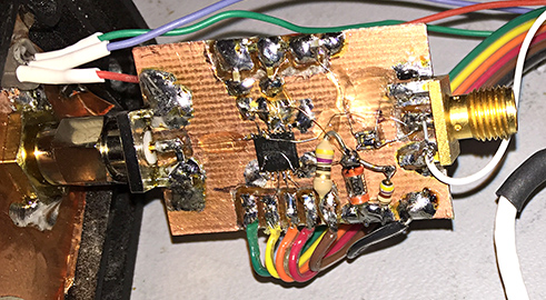

Also, you might try a wider loop BW to begin with, say 1000 Hz.  Is R1 in series with the charge pump output?  If R1 is 60K and Vp is +5, your charge pump current can't exceed about 80 microamps, regardless of the Rset resistor or Icp register values.  So the loop may be OK in theory but not in practice.  Post your ADISimPLL file if you like.

Edit: Another pitfall that's not in the book is that those ceramic SMT capacitors like the 0603 (or 0402?) part you have between pins 4 and 5 are hard to hand-solder reliably.  The end terminations like to detach without leaving any visual evidence.  If the cap survives soldering, it may also open up due to differential thermal expansion during normal operation if a small length of wire isn't used as a strain relief.  Not too likely here, but if (e.g.) one end of the cap were soldered to a ground plane and the other connected directly to an IC pin, thermal stress would be a concern. 

So you might unsolder the capacitor to make sure it's actually OK.  Afterward, use a new capacitor, rather than reinstalling the old one.

« Last Edit: October 30, 2021, 05:50:31 am by KE5FX »
 

Offline YrrahTopic starter

  • Contributor
  • Posts: 25
  • Country: nl
Re: PLL design with ADF4001 does not work
« Reply #8 on: October 30, 2021, 08:31:21 am »

Can you please publish the link, John?
Quote
For example, here's an ADF4002 with a small 38.4 MHz VCXO just to the right of it (click for much larger version):
Thanks, H
 

Offline YrrahTopic starter

  • Contributor
  • Posts: 25
  • Country: nl
Re: PLL design with ADF4001 does not work
« Reply #9 on: October 30, 2021, 09:17:21 am »
Here are my register values.
  Reg00 = 0x100640;       // Ref Counter div 400
  Reg01 = 0x0FA001;       // N Counter div 4000
  Reg02 = 0x0078A6;       // Function Latch: counters held in reset (0x1FF8A6)
  Reg03 = 0x0078A2;       // Function Latch: normal operation (0x1FF8A2)
  Reg04 = 0x1FF8A3;       // Init latch....

I use the "Counter Reset Method" as per datasheet. Init latch is not used.
 

Offline YrrahTopic starter

  • Contributor
  • Posts: 25
  • Country: nl
Re: PLL design with ADF4001 does not work
« Reply #10 on: October 30, 2021, 10:20:36 am »
Please find attached the SIMPLL file. Change extension to pll, please.
 

Offline G0HZU

  • Super Contributor
  • ***
  • Posts: 3015
  • Country: gb
Re: PLL design with ADF4001 does not work
« Reply #11 on: October 30, 2021, 05:27:48 pm »
The nearest I've got here is an old ADC clock circuit. This has a VCXO that runs at 102.4MHz and it uses the ADF4001 and a 10MHz ref.

I think the PD freq is 400kHz and the VCO gain is 1.3kHz/V on the schematic.

I can post up my registers and loop filter if that helps? I'm pretty sure this programs the INIT register first then the  R register followed by the N register and that's it.

It says -100dBc/Hz at 10Hz and also at 100Hz on my schematic so the loop BW must be about 50-100Hz. It locks up fine, I just tried it. At a push I could feed it a 10.24MHz ref and then program the N divider to be the same as yours.

I can then post up the PLL registers for you.
 

Offline KE5FX

  • Super Contributor
  • ***
  • Posts: 1889
  • Country: us
    • KE5FX.COM
Re: PLL design with ADF4001 does not work
« Reply #12 on: October 30, 2021, 06:50:52 pm »
Can you please publish the link, John?
Quote
For example, here's an ADF4002 with a small 38.4 MHz VCXO just to the right of it (click for much larger version):
Thanks, H

There isn't a link to a Web page, just the photo at http://www.ke5fx.com/4002lg.jpg .  Is it not showing up?

The photo is a 10 MHz reflock circuit for the original bladeRF SDR which replaces the onboard 38.4 MHz clock.  Basically the same thing you're doing at 100 MHz.  Ground integrity was important in both the analog and digital areas of that circuit.  I had a lot of trouble with trashed registers when connecting and disconnecting external cables, until I went back and bonded the bladeRF board, AVR controller board, and the PLL board itself securely to the metal enclosure.

Please find attached the SIMPLL file. Change extension to pll, please.

That's messed up.  C1 is 1.0 fF (femtofarads) and it's giving you an error message: "Error 608:  VCO input capacitance too large for this design.  Processing Terminated due to error."  Your VCO doesn't have 100 nF of input capacitance across its tuning port (and if it does, you probably want to use a different one.)  If you fix that, you should get a more realistic value for C1.  That's the capactive element in your dominant pole, so it needs to be calculated properly or nothing else will work.
 

Offline G0HZU

  • Super Contributor
  • ***
  • Posts: 3015
  • Country: gb
Re: PLL design with ADF4001 does not work
« Reply #13 on: October 30, 2021, 07:21:19 pm »
I think my version of ADI SimPLL is too old to read that file.

I quickly wrote some code to reprogram my 102.4MHz VCXO circuit here. The original doesn't use my code so I've crudely programmed the PIC to spit out these register values in this order:

INIT Register 0x0D8093
R Register      0x100064         ; divide by 25 for 400kHz
N Register     0x010001          ; divide by 256 for 400kHz


The SimPLL file is attached although I created this quite quickly.

It shows my loop filter values and this does lock up just fine.

However, if I had a 100MHz VCXO like you I think the registers would be:

INIT Register 0x0D8093
R Register      0x100064         ; divide by 25  for 400kHz
N Register     0x00FA01          ; divide by 250 for 400kHz
« Last Edit: October 30, 2021, 07:24:15 pm by G0HZU »
 

Offline YrrahTopic starter

  • Contributor
  • Posts: 25
  • Country: nl
Re: PLL design with ADF4001 does not work
« Reply #14 on: October 31, 2021, 02:01:03 pm »
I apologize: the file is wrong indeed. I thought I had saved the correct file. However, if you set the Loop Bandwidth to 10 Hz it can deal with the 100 nF input capacitance of the VCXO. C1 gets 31 nF on top of the 100 nF. R1 gets 60.7 kohm and C2 is 633 nF. It still does not work however. I prefer not to modify the VCXO as it is part of my Phase Noise testset, where it works great in another PLL (with active loopfilter). Besides, it has fairly low PN of its own, as measured on a FSWP (by Rohde and Schwartz).
I tried G0HZU suggested settings at a pfd of 400 kHz in a different initialization procedure (Initialization Latch Method) but that still does not work: no lock. I do not know what to do next. A friend will come over next week. We'll see together.
Thanks for all the suggestions in any case.
 

Offline G0HZU

  • Super Contributor
  • ***
  • Posts: 3015
  • Country: gb
Re: PLL design with ADF4001 does not work
« Reply #15 on: October 31, 2021, 02:12:30 pm »
I'm not sure what to suggest but see below for a data grab of my SPI output from the PIC. Have you made sure your SPI data is OK?

The person who designed my 102.4MHz VCXO board did not use a PIC with SPI connections so I had to bit bang the SPI. See below for my SPI data for the 102.4MHz VCXO with an external 10MHz reference. This was captured with an Analog Discovery 2 using the SPI decode within the logic analyser program.
You can see it clocks out the registers as below.

INIT Register 0x0D8093
R Register      0x100064         ; divide by 25 for 400kHz
N Register     0x010001          ; divide by 256 for 400kHz

This locks the PLL reliably for my board. This does show that the INIT>>R>>N register method of programming can be successful.

I also tried these register values with an external 10.24MHz reference and it locked fine as well.

INIT Register 0x0D8093
R Register      0x100064         ; divide by 25  for 400kHz
N Register     0x00FA01          ; divide by 250 for 400kHz


Offline G0HZU

  • Super Contributor
  • ***
  • Posts: 3015
  • Country: gb
Re: PLL design with ADF4001 does not work
« Reply #16 on: October 31, 2021, 04:58:47 pm »
I guess you've checked this already but if the VCXO only has a tuning range of +/- 2.5kHz then the 10MHz external reference has to be within +/- 250Hz of a true 10MHz assuming your VCXO can accurately tune either side of an accurate 100MHz.

So a crystal oscillator based 10MHz reference might not be accurate enough for the loop to lock. What are you using for a 10MHz reference?

Also what DC voltage do you have at Vp for the charge pump? On my circuit here the AVDD and DVDD are both 3V3. Vp is 5V to allow a good margin for the charge pump current to be generated correctly at a (say) 2.6V tuning voltage.
« Last Edit: October 31, 2021, 05:03:31 pm by G0HZU »
 

Offline YrrahTopic starter

  • Contributor
  • Posts: 25
  • Country: nl
Re: PLL design with ADF4001 does not work
« Reply #17 on: October 31, 2021, 08:13:42 pm »
The sketch I use is derived from a sketch from a friend for the ADF5355. That works, I know because I use it. It is simplified because the ADF4001 needs less registers. The structure is the same. So after your very valuable remark I compared the timing of the 5355 with the 4001, as per datasheet. The timing of the 5355 is similar but faster. The Arduino is working at 16 MHz, so the fastest clock pulse can only be about 60 nsec, right? All else equal I guess timing is no issue. I have no way to check that in situ, unfortunately.
For the moment the reference is my Agilent 8664A, within a Hz. Checked with a HP5345A. However, a little below 10.00MHz (say 7-10 kHz) I found some activity at the output of the 4001. No lock but looks like its trying. Very strange.
In my setup all three voltages are connected to the +5V from the Arduino. This is, of course, only for testing. In the final application I will be using a low noise +5V source. At 2.125V the VCXO is at 100 MHz. The Arduino is connected to a laptop via USB, so all is USB powered.
Thanks a lot for your time and patience.
 

Offline G0HZU

  • Super Contributor
  • ***
  • Posts: 3015
  • Country: gb
Re: PLL design with ADF4001 does not work
« Reply #18 on: October 31, 2021, 08:35:55 pm »
One other thing to consider is how quickly your Arduino sketch starts sending out SPI code from the AVR MCU. In my case I added quite a long delay in the PIC code before sending out the SPI. This allowed time for the supplies to settle. There are also various options in the control registers for brownout and possibly a power-up timer to try and prevent power up issues like this.

In my case I didn't get to choose the MCU. It is a 16F688 PIC and there are lots of traps for the unwary with this chip, especially because it has analogue/comparator/digital options in the control registers for the I/O ports. Get these control registers wrong and the chip can behave in strange ways. I much prefer AVR because I like to program in assembly language and the AVR instruction set is more suited to me.

Is there any way the USB interface can cause your system to corrupt the ADF4001 registers shortly after you program them?

« Last Edit: October 31, 2021, 08:42:02 pm by G0HZU »
 

Offline G0HZU

  • Super Contributor
  • ***
  • Posts: 3015
  • Country: gb
Re: PLL design with ADF4001 does not work
« Reply #19 on: November 01, 2021, 05:48:24 pm »
I quickly measured the 102.4MHz VCXO PLL output on an E5052A signal analyser and took two plots. One is when the PLL is locked and one when it is not.

In the locked state the phase noise does look very similar to the SimPLL simulation where the phase noise is about -100dBc/Hz at 10Hz and the loop bandwidth is just under 100Hz.
 

Offline YrrahTopic starter

  • Contributor
  • Posts: 25
  • Country: nl
Re: PLL design with ADF4001 does not work
« Reply #20 on: November 02, 2021, 08:55:35 am »
Nice measurements! I hope some day I can have the same results. I will look today with a friend. Must be something obvious or stupid. Will come back here.
My best, H
 

Offline YrrahTopic starter

  • Contributor
  • Posts: 25
  • Country: nl
Re: PLL design with ADF4001 does not work
« Reply #21 on: November 03, 2021, 10:49:05 am »
It works!
The point is: you can not rely on the MUX output to observe the R and N counter input levels. The N counter output remains stable between less than -10 dBm until as high as +1 dBm and is quite tolerant about level. The R counter behaves almost the same but to establish reliable lock you need to provide at least +1 dBm. I operate the ADF4001 at +5V and then you need even more input signal (voltage). Refer to note 2 of datasheet, page 2. For the record: R Divider pulse width: 100 nsec, N Divider pulse width: 10 nsec.
To establish lock the CP cap is quite indifferent. I get lock from 100 nF to 100 uF. Of course loop dynamics is completely different....
Thanks to you for your comments. Highly appreciated.
 

Offline G0HZU

  • Super Contributor
  • ***
  • Posts: 3015
  • Country: gb
Re: PLL design with ADF4001 does not work
« Reply #22 on: November 03, 2021, 07:48:19 pm »
Sounds good now!

Your phase noise measuring stuff sounds interesting. I'm tempted to try this 102.4MHz VCXO to clock a fast DDS to see if the DDS can deliver low phase noise at output frequencies up to maybe 20MHz. I've got a couple of high performance spectrum analysers that can measure phase noise (in SSA mode) but the performance is a bit lacking in this respect. At work I have access to a couple of E5052A SSAs but I'd like to make something for home use too.


Offline YrrahTopic starter

  • Contributor
  • Posts: 25
  • Country: nl
Re: PLL design with ADF4001 does not work
« Reply #23 on: November 05, 2021, 02:19:45 pm »
For phase noise measurements at oscillators I have built a Phase Noise Testset by an article from DG4RBF, UKW-Berichte 4/2015. Not particularly easy to construct but it works good. Normal spectrum analyzers can not be used for serious phase spectrale analyses, as you know.
But this is another story....


Share me

Digg  Facebook  SlashDot  Delicious  Technorati  Twitter  Google  Yahoo
Smf