Author Topic: JLCPCB - inner layers done as a positive not negative  (Read 399 times)

0 Members and 1 Guest are viewing this topic.

Offline peter-hTopic starter

  • Super Contributor
  • ***
  • Posts: 5245
  • Country: gb
  • Doing electronics since the 1960s...
JLCPCB - inner layers done as a positive not negative
« on: December 04, 2025, 07:01:22 pm »
No inner planes :)


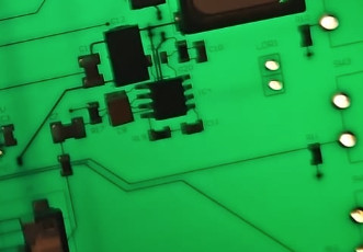
What I don't get is why they have made an almost identical board correctly a few weeks back, as well as all the other 4-layer boards, and their BBT test passes connectivity which obviously does not exist.

because orders be divided to different engineers each time, the engineer may did not notice it somtimes. to avoid misunderstanding, we recommend leaving remarks about the negative layers when ordering..

I had a bit of fun getting these boards to run ;)

we recommend exporting files in positibe layers, if there has negative copper layers, better to leave remarks to remind our engineers in the future

but I have never seen PCB software which does layers as positive e.g. filled polygons or some such.

I have been using PCBWAY for 3D printing. Their PCB quote is a lot more than JLCPCB, and while they do have a gerber viewer, it doesn't show planes.

ALLPCB is same price as JLCPCB and no gerber viewer.  They refer me to their domestic website https://www.jiepei.com/ but that one doesn't translate well enough (in Chrome) to use.

It is many years since I had a screwup like this. These used to happen in the UK from time to time, with e.g. all holes plated through on every via, so the whole board was totally shorted.
« Last Edit: December 04, 2025, 07:44:19 pm by peter-h »
Z80 Z180 Z280 Z8 S8 8031 8051 H8/300 H8/500 80x86 90S1200 32F417
 

Offline AndyC_772

  • Super Contributor
  • ***
  • Posts: 4415
  • Country: gb
  • Professional design engineer
    • Cawte Engineering | Reliable Electronics
Re: JLCPCB - inner layers done as a positive not negative
« Reply #1 on: December 04, 2025, 08:02:25 pm »
but I have never seen PCB software which does layers as positive e.g. filled polygons or some such.

Seriously?

I've not even seen a negative plane in years. I use OrCAD, filled polygons are exactly what you get in the Gerber output by default.
 
The following users thanked this post: Smokey, thm_w

Offline langwadt

  • Super Contributor
  • ***
  • Posts: 5398
  • Country: dk
Re: JLCPCB - inner layers done as a positive not negative
« Reply #2 on: December 04, 2025, 08:08:20 pm »
but I have never seen PCB software which does layers as positive e.g. filled polygons or some such.

Seriously?

I've not even seen a negative plane in years. I use OrCAD, filled polygons are exactly what you get in the Gerber output by default.

yeh, negative planes is just a legacy from the times of using tape, easier to put a circle and invert than  to tape the whole plane

see no reason to use it anymore
 

Offline peter-hTopic starter

  • Super Contributor
  • ***
  • Posts: 5245
  • Country: gb
  • Doing electronics since the 1960s...
Re: JLCPCB - inner layers done as a positive not negative
« Reply #3 on: December 04, 2025, 08:46:51 pm »
Let's take an example. In Protel PCB a pad can have a "relief" and you can choose Plane 1, Plane 2, etc.

If you choose 1 and 2 then every PCB company I have ever used (probably dozens) will realise there are two inner layers.

And sure enough when you upload the design to any of these firms (just done 3 tonight) they correctly state "4 layer".

The other interpretation of the relief shape is meaningless because it (the 2 or 4 "fingers") goes nowhere, and has no electrical connectivity to anywhere. I can see the BBT test will pass because it references the meaningless gerber so of course it will pass ;)

I've been using PCB CAD since 1991 and have not seen this issue before.
« Last Edit: December 04, 2025, 09:07:44 pm by peter-h »
Z80 Z180 Z280 Z8 S8 8031 8051 H8/300 H8/500 80x86 90S1200 32F417
 

Offline jc101

  • Frequent Contributor
  • **
  • Posts: 798
  • Country: gb
Re: JLCPCB - inner layers done as a positive not negative
« Reply #4 on: December 04, 2025, 09:27:44 pm »
I've just ordered a 6 layer board from PCBWay. Recent batches of the same board from JLCPCB have had odd traces that have a break along the path somewhere internal. Despite them all apparently passing a full electrical test. Managed to bridge with a tiny wire between vias. Naturally, I find the problem once the PCB is assembled. It a very busy double sided load, so saving the board is worth while.

Despite PCBWay cost more, I don't mind if I don't end up chasing a PCB issue.
 

Online Whales

  • Super Contributor
  • ***
  • Posts: 2474
  • Country: au
    • Halestrom
Re: JLCPCB - inner layers done as a positive not negative
« Reply #5 on: December 04, 2025, 09:48:15 pm »
I do not believe JLCPCB does "100%" electrical testing, despite their claims.  I once received boards where a couple had clear gashes through them that cut some top traces.  The cut copper surfaces looked like they were done before the end of the pcb fab process, because of a mix of them being plated & unplated, I'll have to dig and see if I can find the photos, my memory is rough.

EDIT: Retract that, looks like the gash was through a GND plane and didn't cut any traces, so it would still pass flying probe electrical testing.  Note that the left edge of the gash in the soldermask has plating showing through it, suggesting the damage/contamination was done prior to HASL but after copper.

« Last Edit: December 04, 2025, 10:00:25 pm by Whales »
 

Offline Smokey

  • Super Contributor
  • ***
  • Posts: 3565
  • Country: us
  • Not An Expert
Re: JLCPCB - inner layers done as a positive not negative
« Reply #6 on: December 04, 2025, 11:34:28 pm »
I feel like the soldermask layer is often drawn as a negative layer in CAD.
 

Offline peter-hTopic starter

  • Super Contributor
  • ***
  • Posts: 5245
  • Country: gb
  • Doing electronics since the 1960s...
Re: JLCPCB - inner layers done as a positive not negative
« Reply #7 on: December 05, 2025, 07:52:22 am »
Solder resist is implicitly negative, too. The gerber data is not "cover the whole board except the pads" :)

Would PCBWAY be the recommendation here? The extra cost is almost insignificant for prototyping, and we use totally different firms for production.

Have production hassles too, with dodgy "BBT testing against gerber", but that's another story ;) I have a few boards from a new supplier to hand build at work, before we start populating the 4k circuits...

I will update here on what JLC propose but if they don't re-make the boards, it will be PCBWAY from now on.
« Last Edit: December 05, 2025, 08:05:23 am by peter-h »
Z80 Z180 Z280 Z8 S8 8031 8051 H8/300 H8/500 80x86 90S1200 32F417
 

Offline peter-hTopic starter

  • Super Contributor
  • ***
  • Posts: 5245
  • Country: gb
  • Doing electronics since the 1960s...
Re: JLCPCB - inner layers done as a positive not negative
« Reply #8 on: December 05, 2025, 11:48:11 am »
JLCPCB are re-making the boards:

Thank you for your message, and we are very sorry for the inconvenience caused.

After checking, we confirmed that the inner layers were not converted to positive film due to an engineering mistake. This issue has already been reported to the relevant team, and they will pay closer attention to this in the future.

We have now updated the correct production file. If you place a reorder later, it will follow the corrected data. We recommend selecting the “Confirm Production File” option next time for extra assurance.

May we proceed with remaking the boards for this order?
Z80 Z180 Z280 Z8 S8 8031 8051 H8/300 H8/500 80x86 90S1200 32F417


Share me

Digg  Facebook  SlashDot  Delicious  Technorati  Twitter  Google  Yahoo
Smf