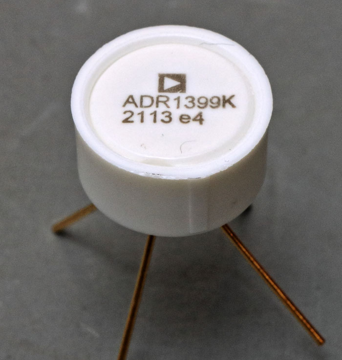
Now let´s take a look into a ADR1399!
Output voltage is 7,05V. The output impedance is lower than that of the LM399: 0,04Ω(typ) / 0,08Ω(max) vs. 0,5Ω(typ) / 1,5Ω(max).
The datasheet states a faster warm up time (0,1s vs. 2s). That´s interesting because the heater current is the same. Looking at the diagrams you see that the ADR1399 heater controller is just faster. There is a nice little overshoot while the LM399 heats slower but evenly.
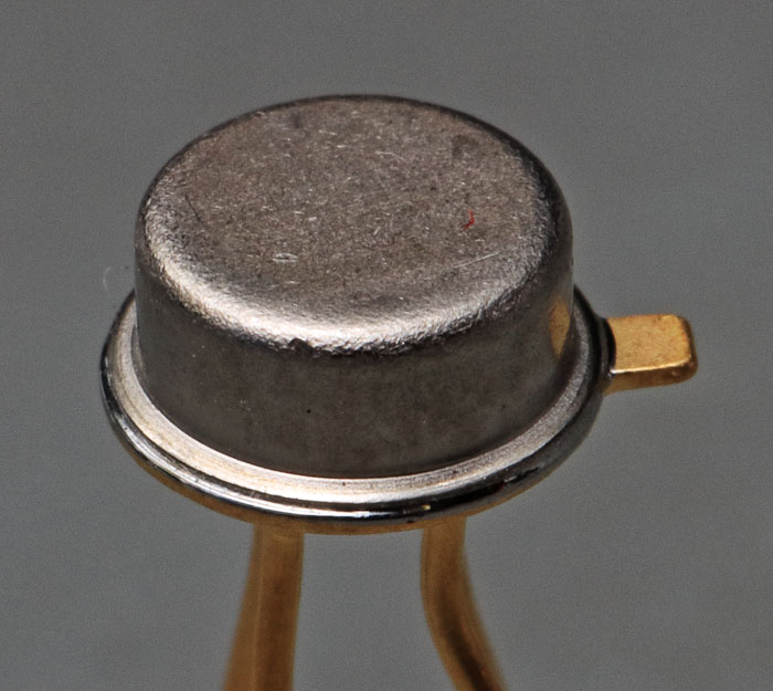
The package looks like the package of the LM399.
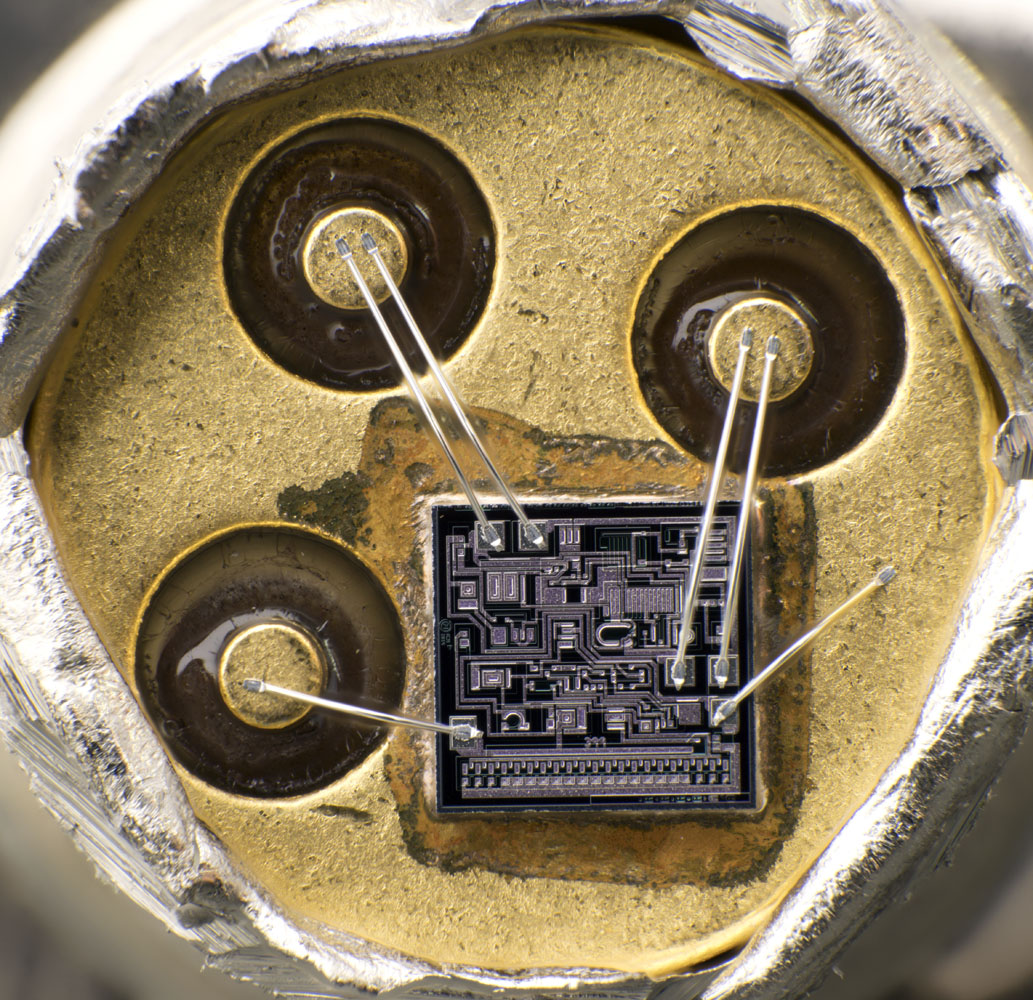
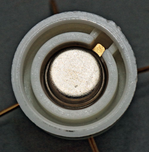
The package and the die look quite similar to the LM399 but there are two bondwires for the shunt regulator.
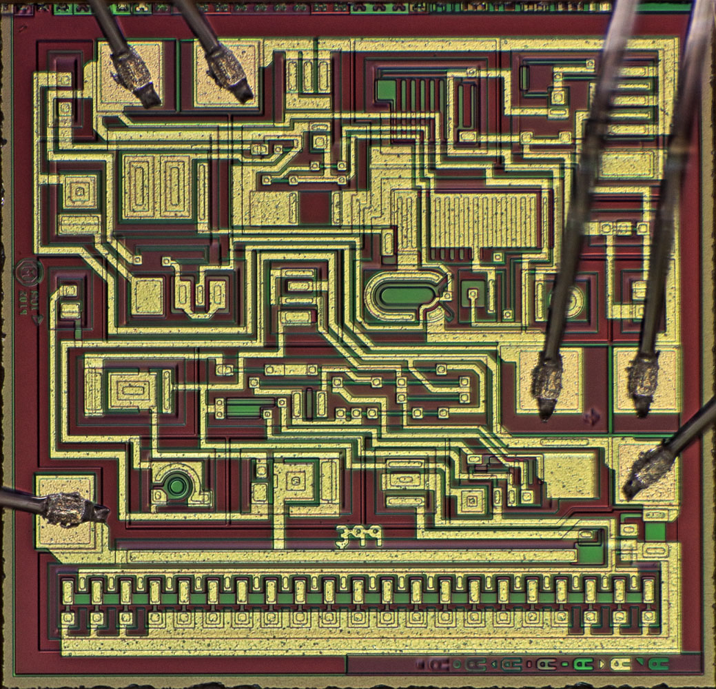
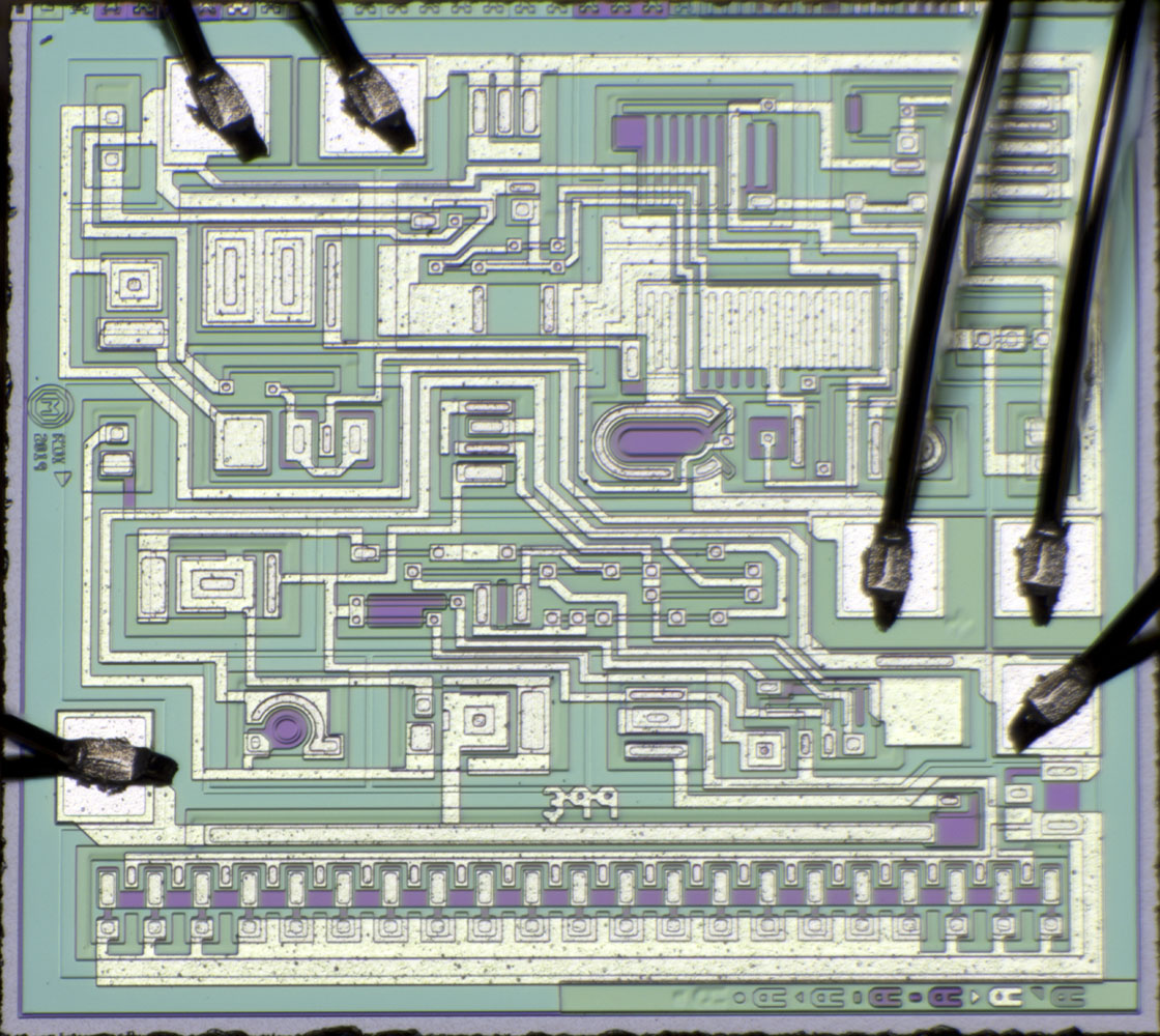
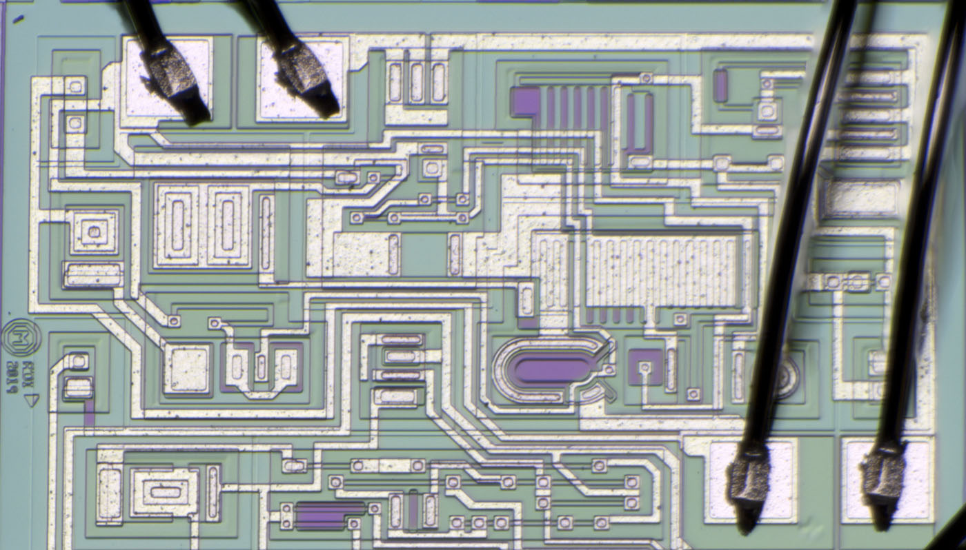
The die looks quite similar to the LM399 but there are some differences. It seems like Analog Devices integrated some new functions while trying to leave the structures as similar as possible.
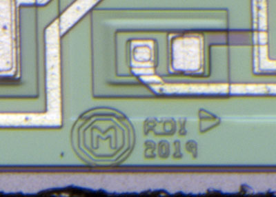
It´s a 399 designed by Analog Devices in 2019.
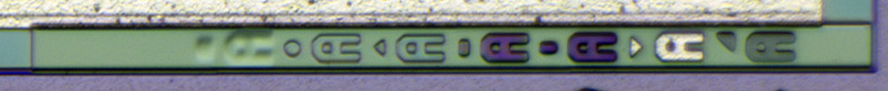
Seven masks like in the LM399. In the ADR1399 all of them are at the lower edge.
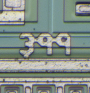
(Have you recognized the different symbols left of the letters? Nice...

)
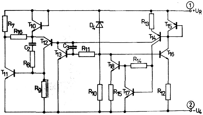
Let´s compare the ADR1399 with the schematic of the MAC199 which shows the LM399 circuit quite accurate.
There are a lot of circuit parts that look like LM399 but some of them are wired differently and some parts were added (red).
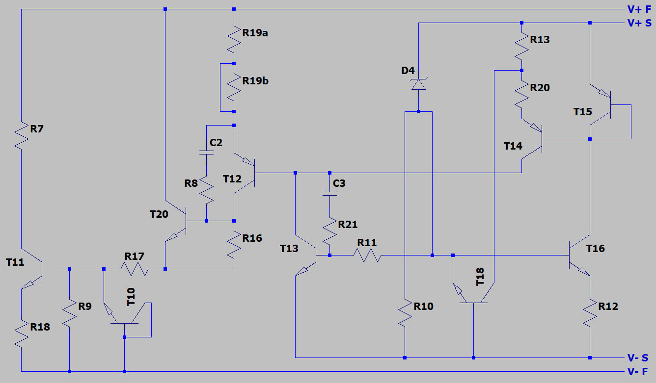
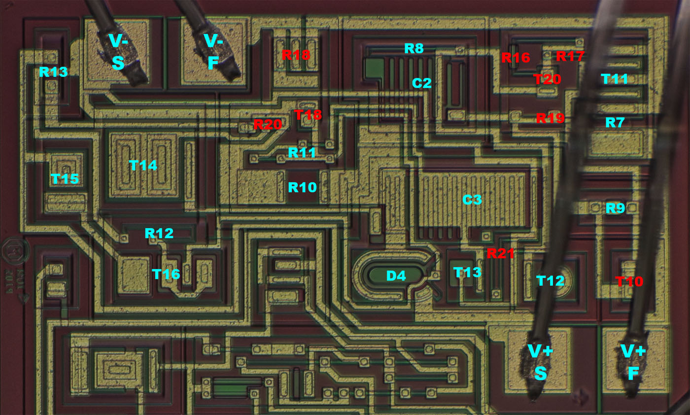
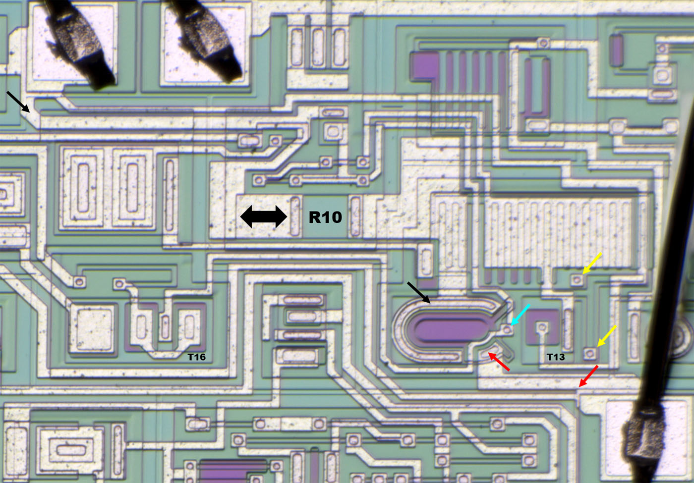
The circuit looks like this. The ADR1399 die allows Kelvin connection. There are two bondpads for the reference and control circuit and there are two bondpads for the power stage.
The zener D4 has an additional contact which makes it possible to connect the reference potential offside the bias current.
The control circuit T13/T16/T15/T14 is similar to the LM399 but here we have no additional current sink.
T18 seems to limit overvoltages that otherwise would cause current spikes that probably would damage the zener. The collector of T18 seems to be connected to R13/R20 coincidentaly. The collector base breakdown voltage is probably too high to be usefull. I assume R20 had just the right position to use its potential for the well of T18.
The output stage got an additional Transistor (T16), now it´s a Sziklai-Darlington-Stage. You probably need the higher current gain for the lower impedance of the shunt regulator.
The overcurrent protection was changed too. T10 drains base current of T11 if the voltage across R18 gets to high.
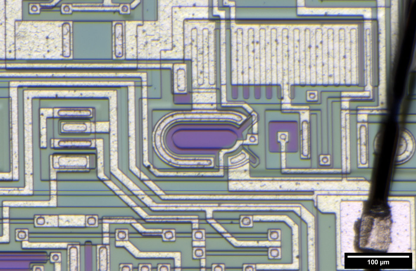
The buried zener is oval. It looks similar to the zeners of the LTFLU (
https://www.richis-lab.de/REF04.htm).
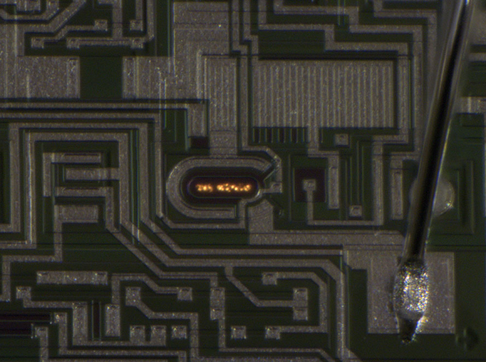
And it glows in the dark...

Due to avalanche breakdown fast electrons lift electrons of the atoms on different higher stages. While falling back into their home position they emit different wavelengths.
The glow is located in the middle of the zener a little under the surface.
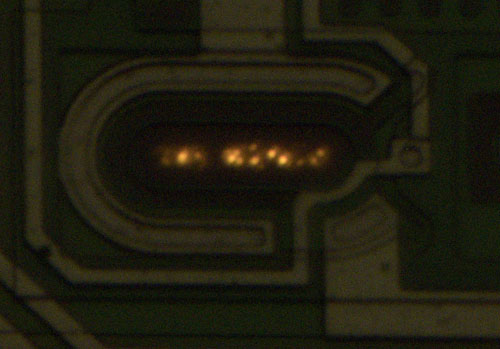
1mA
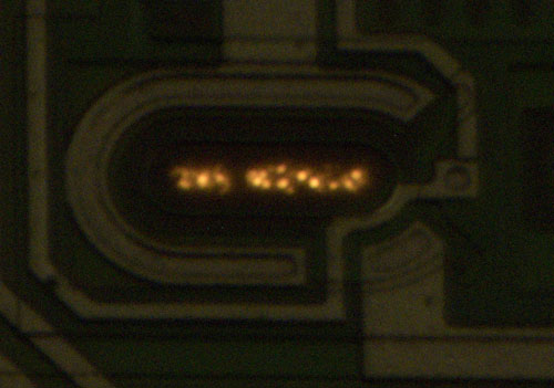
10mA
You can see the individual areas where the breakdown occurs. In the LTZ1000 we saw individual areas too (
https://www.richis-lab.de/REF03.htm). In the ADR1000 the glow was a little more uniform (
https://www.richis-lab.de/REF19.htm).

Here you can see the contact to the upper n-doped area (red). The contact for the bias current (black) and the additional contact for the reference voltage (cyan). It seems like the two "fingers" do some shielding against the additional contact.
R10 is low resistance probably because there is no additional current sink. One contact can be varied for different bias currents.
We have talked about the strange transistors. Magic has told us about tuning them for best performance of the reference. Here we see different but still strange transistors: T16 (left) contains two very big emitter areas. The T13 emitter area is very big too.
On the right side there are two contacts two lower the base resistance of T13 (yellow).
The resistor of the current limit circuit can be tuned a little.
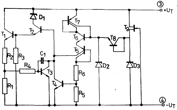
Now let´s take a look at the heater.
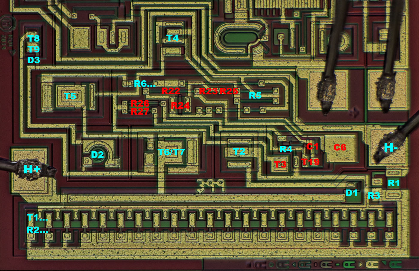
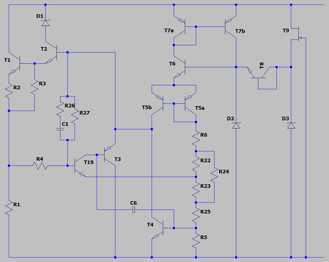
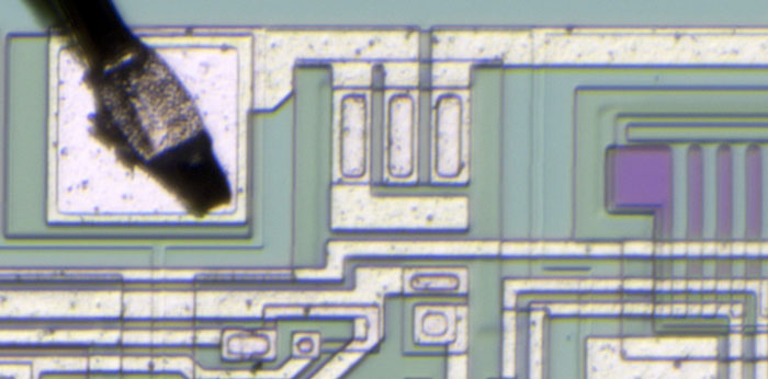
The reference circuit is the same as in the LM399. Just the voltage divider is more complex (R6, R22, R23, R24, R25, R5). T4, the temperature sensing transistor, is equipped with a second base contact. With the voltage divider resistors and the second base contact you can tune the working temperature of the ADR1399.
The heater stage is the same as in the LM399 but the current limiter looks different. T19 is sensing the current through R1 and drives T3. Furthermore T19 sources its emitter current into the voltage divider of T4.
This circuit made it possible to accelerate the heater. At an cold start-up the heater works in current limit mode. T19 drives T3 which sinks current from T1/T2 to limit the current. Emitter current from T19 makes T4 sinking current too. Collector current of T4 increases with temperature. At some point T4 drains enough current to drive T1/T2 out of current limit area. As a consequence T19 sources less current into the voltage divider and T4 sinks a little less current slowing down the decrease in heater current or in other words holding a high heater current for a longer time.
C6 and R26/C1/R27 were probably necessary to prevent oscillations.
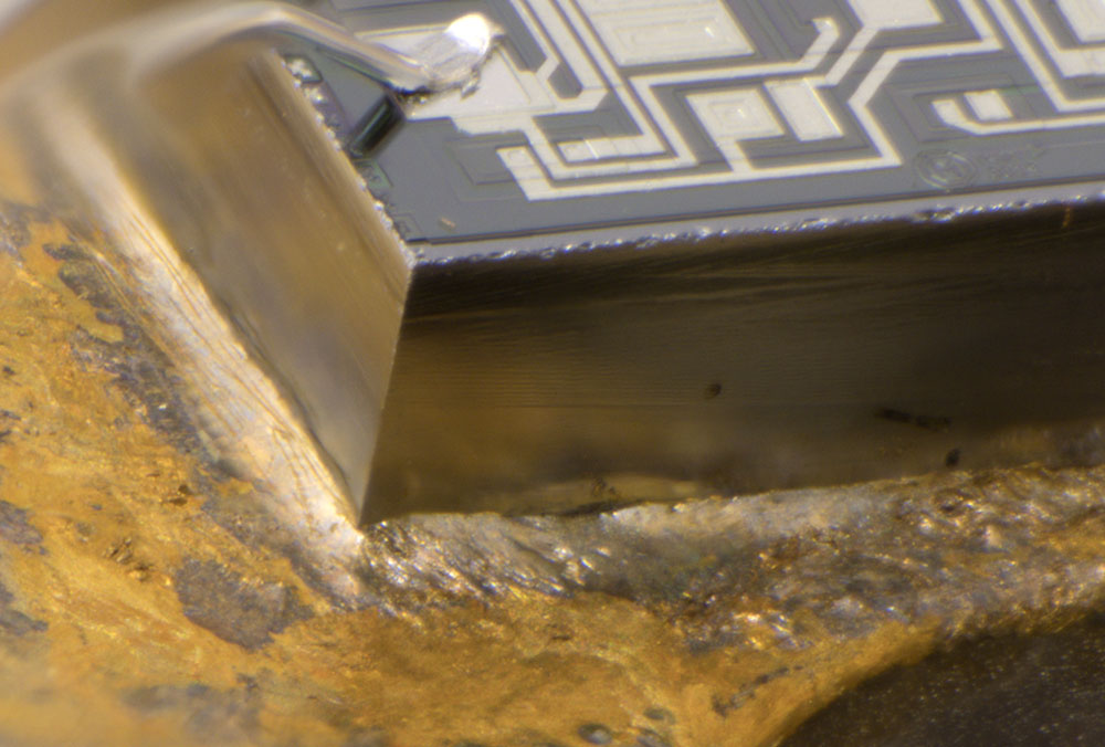
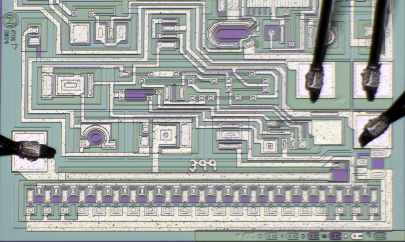
The ADR1399 has been sawn out of the wafer quite nicely while the last bit of the LM399 was broken.
https://www.richis-lab.de/REF20.htm 


