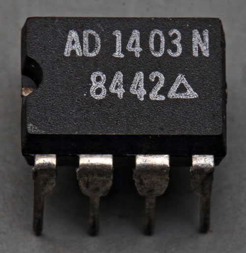
The AD1403 is a low cost 2,5V-reference. Supply voltage needs to be 4,5V and can go up to 40V. The better graded AD1403A guarantees 2,5V+/-10mV. Tempco is typically 10mV/°K. It can source 10mA.
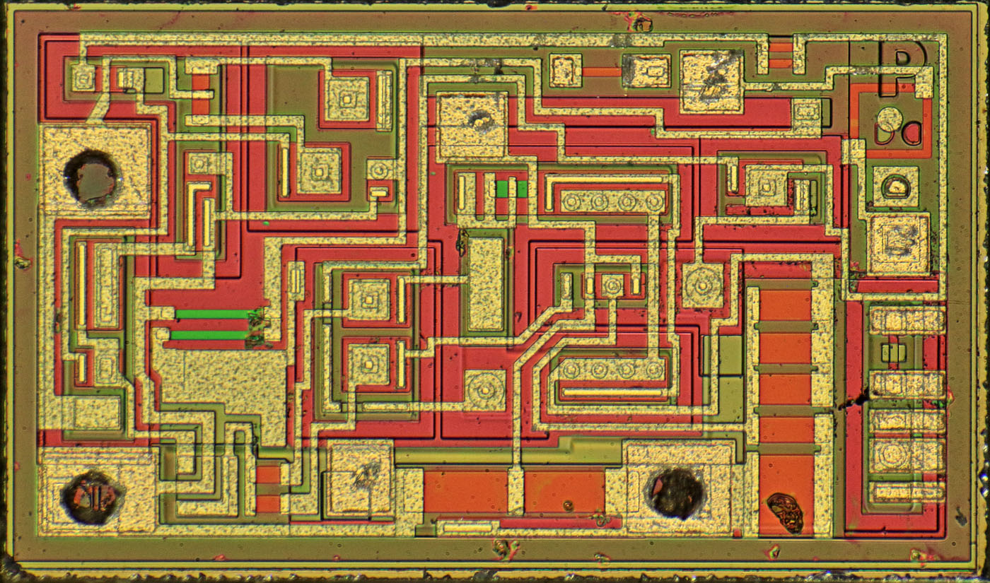
The die is 1,5mm x 0,9mm.
There is a testpad connected to the bondpad in the left corner. Would be interesting why that testpad was necessary. It would have been possible to connect the potential at the bondpad.

The big orange resistors can be laser trimmed.
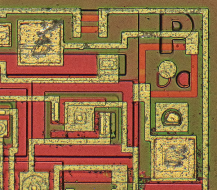
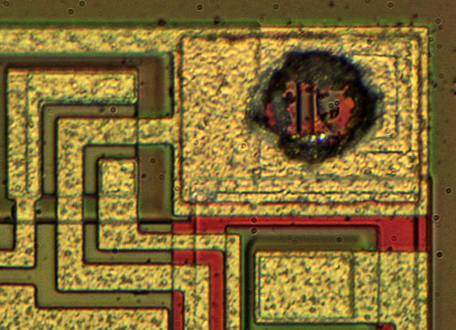
In the upper right corner there are two testpads that are just connected to a orange square. You often see such structures on dies with tunable resistors.
You can´t see any tuning. That´s interesting. Normally the laser tracks are visible. The tolerance of semiconductor resistors are quite high. I´m pretty sure the AD1403 needed some trimming.
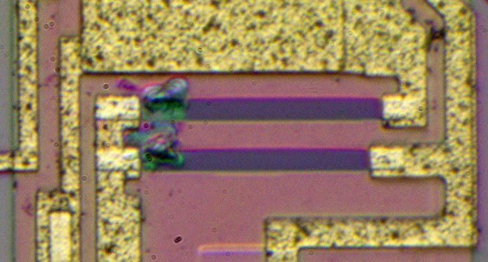
Even more interesting is this "residue" on two smaller resistors which are built with a different material. That looks quite like laser trimming. You can even see some trenches. But usually you only trim the resistors that are designed for trimming. And tunable resistors are usually bigger to make trimming easier. Strange...
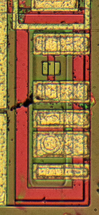
Two test structures. The upper structure is a pinch resistor, the lower one is a npn-Transistor.
Interesting point here: On top of the p+ doped trench that isolates the active areas is a red layer. The red layer is the p doped base material. It seems like Analog has used the same technique as National used in the output transistor of the LM306 (
https://www.richis-lab.de/Opamp09.htm). The less p doped base layer gives you a higher breakdown voltage between the active area and the substrate.
There seems to be an active element under the output bondpad. Perhaps some overvoltage protection...
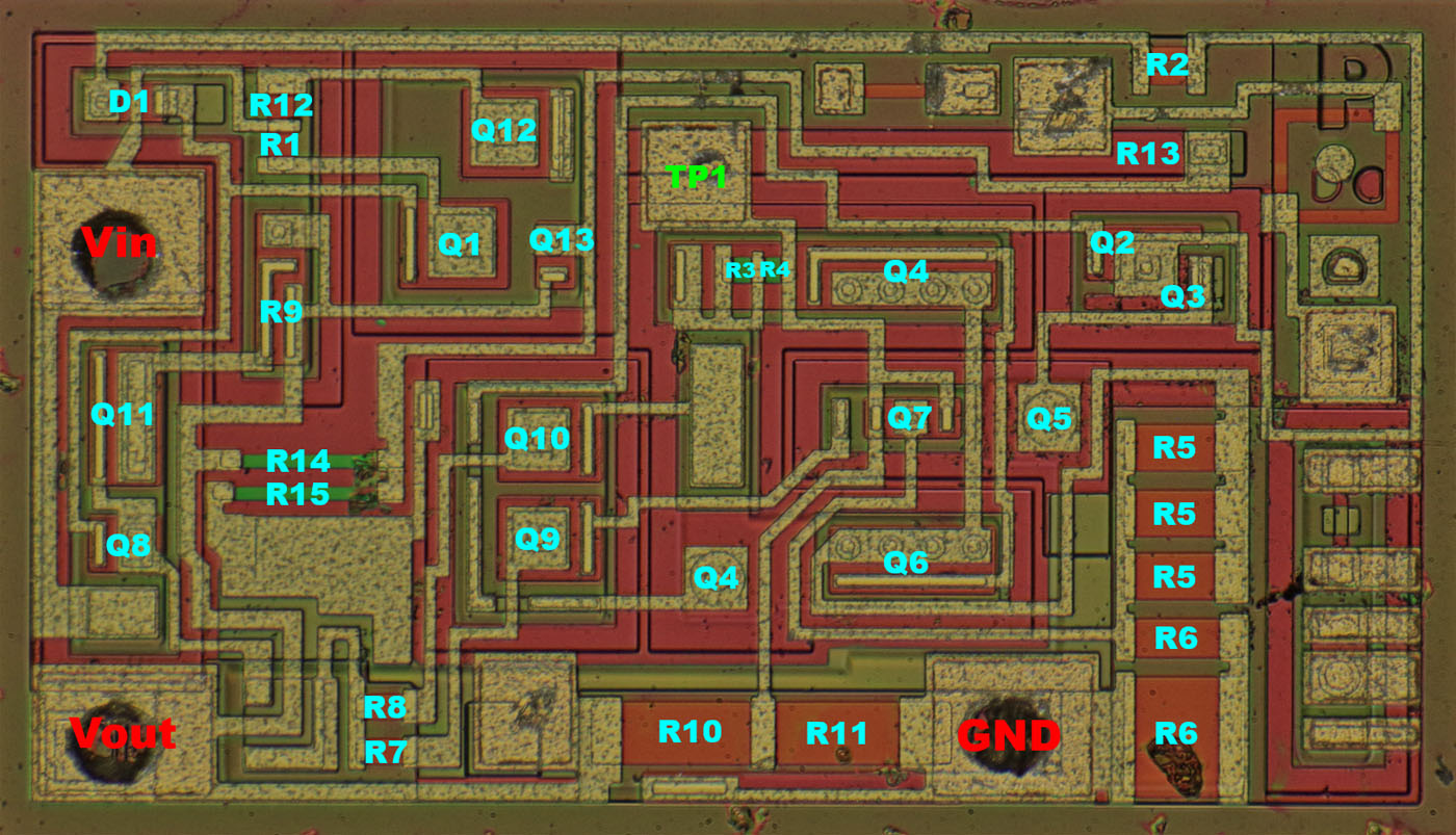
Identifying the different components is no bigger problem but there are some interesting structures...
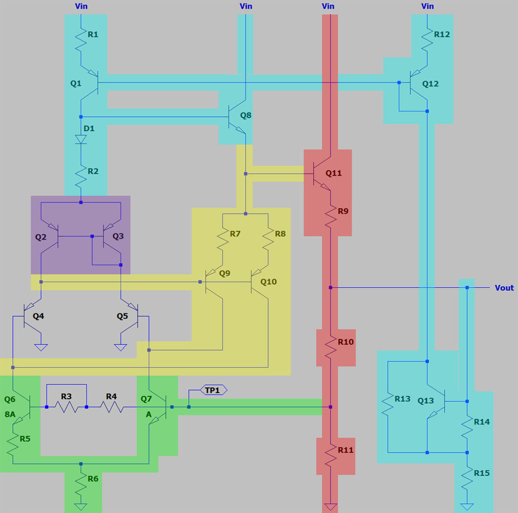
The cyan parts are the bias circuit. Q13/R14/R15 are taking the output voltage and generating a reference current. R13 is for proper start-up. R14/R15 are the small tuned resistors. That makes some sense. There is a current regulation around the bandgap cell but it´s probably a good thing to adjust the supply current to a value near the optimum.
The green area is the bandgap cell with the transistors Q6/Q7 having different areas. R5 and R6 are tunable to adjust the tempco to an optimum. With the help of the testpad 1 you can meassure the voltage while tuning the circuit.
Q2/Q3 ist a current mirror which wants equal currents in the two legs. If there are different currents Q9/Q10 are adjusting Q11 so the voltage at the bandgap-reference base goes to a level where the currents are equal and the bandgap-reference works as intended.
There are two interesting facts: The collector currents of Q9 and Q10 are directed into the bandgap-reference. And there are the two pnp-transistors Q4/Q5 which act like small amplifiers for the bandgap currents.
The whole circuit looks like they had put a lot more effort in than it looks like in the first place. I´m sure there are some smart tweaks hidden in the schematic.
The red part is the regulation loop and the output stage. R10/R11 gives you the voltage you like. Because of that R10 and R11 are tunable.
R10 adds some drift effects to the reference voltage. That drift is compensated with R3/R4. R3 is shorted with the metal layer. Perhaps there was an option to adjust R10/R11 to a different output voltage that would have needed R3.
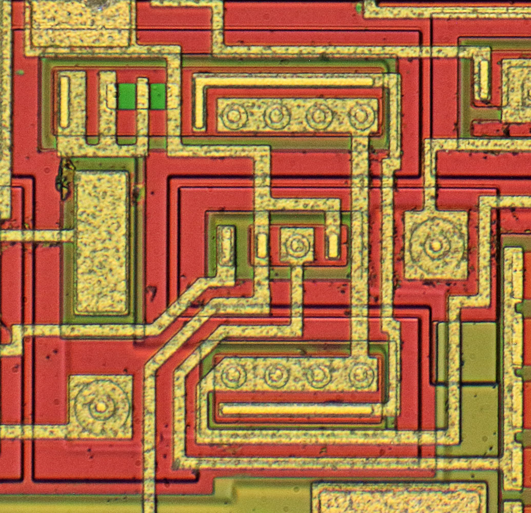
Here you can see the bandgap transistors with an area of 8:1. The bigger transistor is built with two four-emitter transistors surrounding the small one-emitter transistor.
In the red p-doped areas connected to ground there are the two pnp-transistors Q4/Q5 interacting with the collector area of the bandgap transistors.
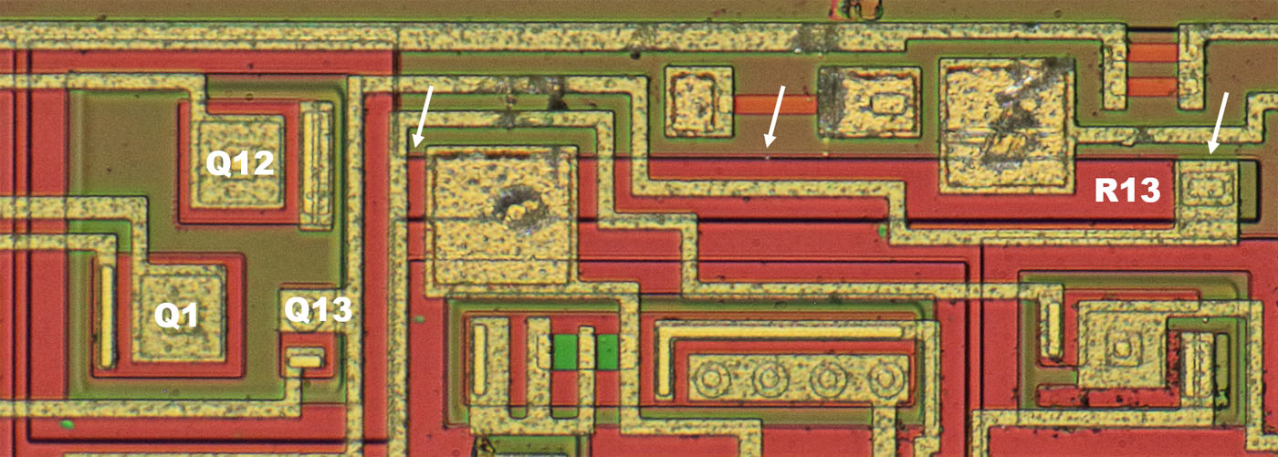
R13 is quite interesting. The collector area is shaped into a stripe building R13.
 https://www.richis-lab.de/REF16.htm


