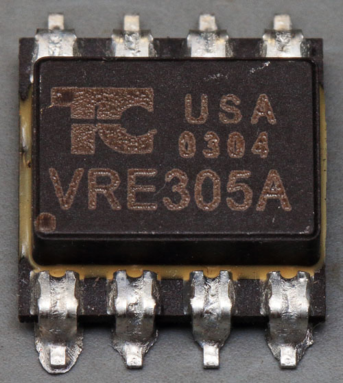
The VRE305A is a voltage reference developed by Thaler Corporation, now sold by Apex. Several variants exist with different output voltages from 2.5V to 10V, different packages and slightly different specifications.
The VRE305A delivers 5V with an initial tolerance of +/-0.5mV max and a temperature drift of 0.6ppm/K max. The long-term drift is 6ppm/1000h typ. The supply voltage must be at least 13.5V.
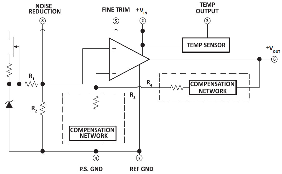
The datasheet contains a schematic that explains the operation of the VRE305A. The basis of the reference voltage is a 6.3V z-diode whose operating current is supplied by a JFET current source. A capacitor can be connected externally at pin 8 to reduce noise.
An opamp sets the desired output voltage with its gain factor. Resistors R3/R4, which define the gain factor, each contain a compensation network. According to the datasheet, this is a mixture of resistors and thermistors set to minimize the temperature drift of the reference voltage. The thermistors each make up just 2% of the total resistance so that they have as little effect as possible on the long-term drift.
Apparently one wanted to avoid setting the output voltage of the different variants by the resistor ratio R3/R4 and therefore integrated the voltage divider R1/R2 between the z-diode and the opamp. Pin 5 allows to adjust the output voltage a little. Other than shown in the schematic, this input influences the inverting input of the opamp. The VRE305A offers an additional ground pin, which allows to tap the reference voltage unloaded.
As will be shown in a moment, the temperature sensor is a simple diode whose operating current is set by a resistor.
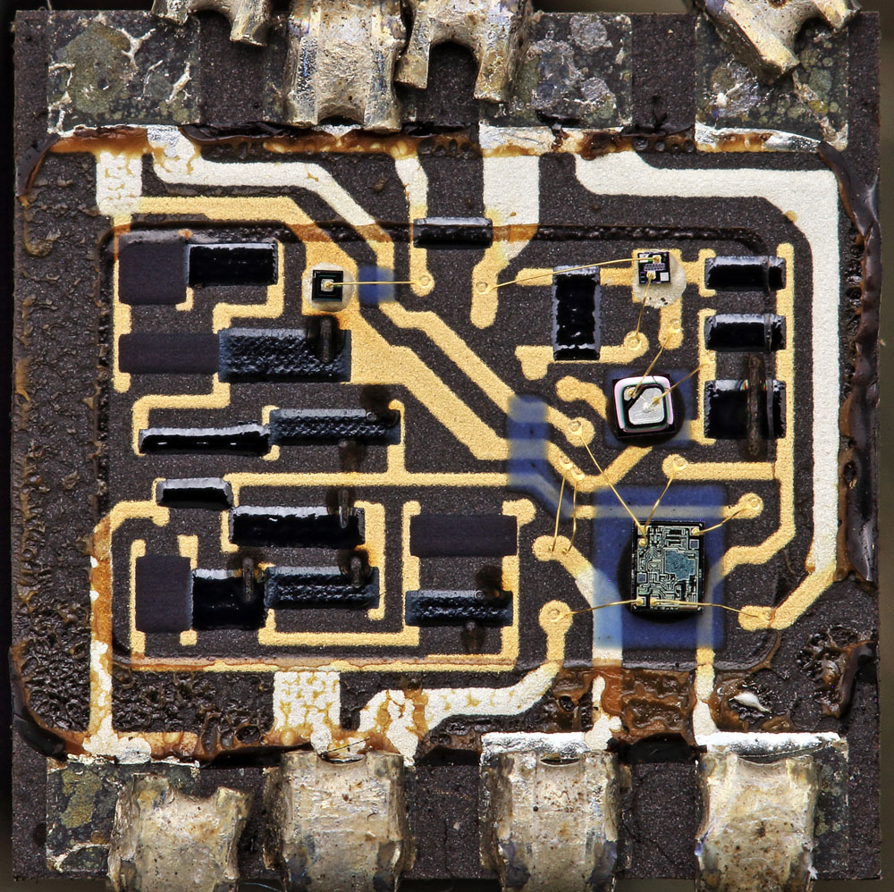
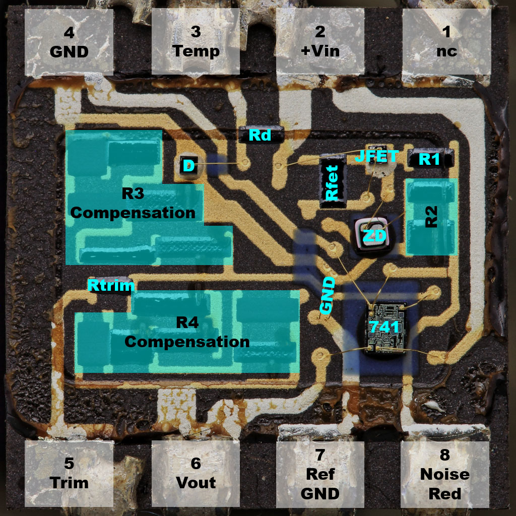
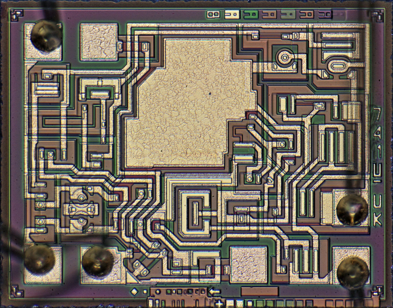
Under the cover there is a hybrid circuit. A large part of the area is taken up by the resistors R3/R4 with their compensation networks. The trim input influences the node between the resistors R3/R4 via the resistor Rtrim. The inverting input of the opamp is connected to this node too. The opamp is a National Semiconductor LM741. It has its own GND feed line.
The reference voltage source is located in the upper right corner of the board. The construction is the same as shown in the datasheet. The resistor R2 is divided into two areas of different size. Apparently these resistors are used to represent the different output voltages with little effort.
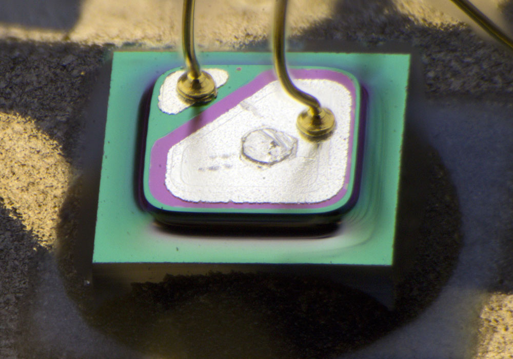
Pin 7, which is the GND for the reference voltage, is connected with two bonding wires to the z-diode so that this path is loaded as little as possible by the bias current of the diode.
At the top edge of the board is the diode, which can be used for temperature measurement. The resistor Rd provides the bias current.
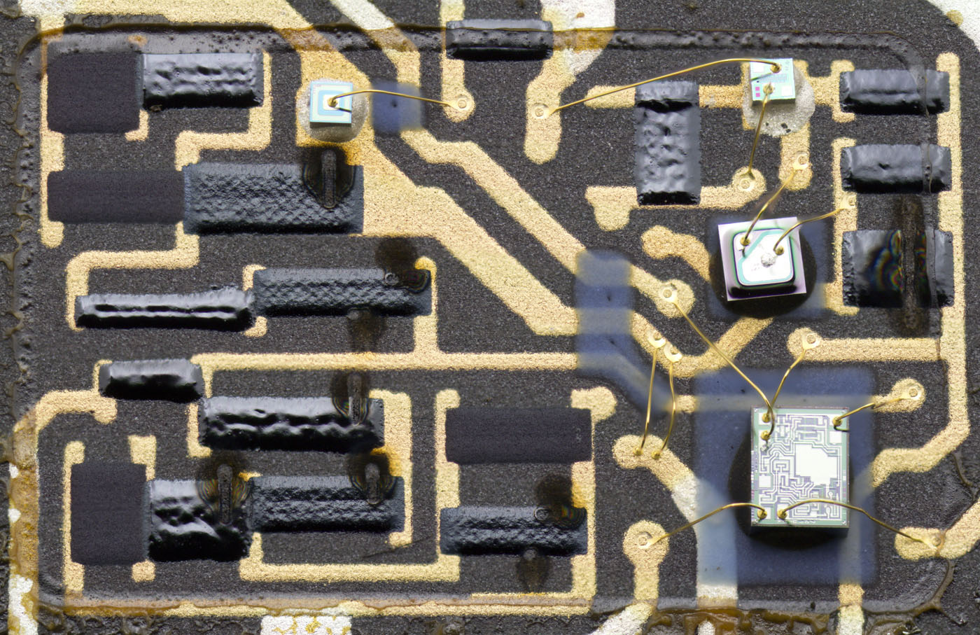
A lot of the resistors were laser tuned.
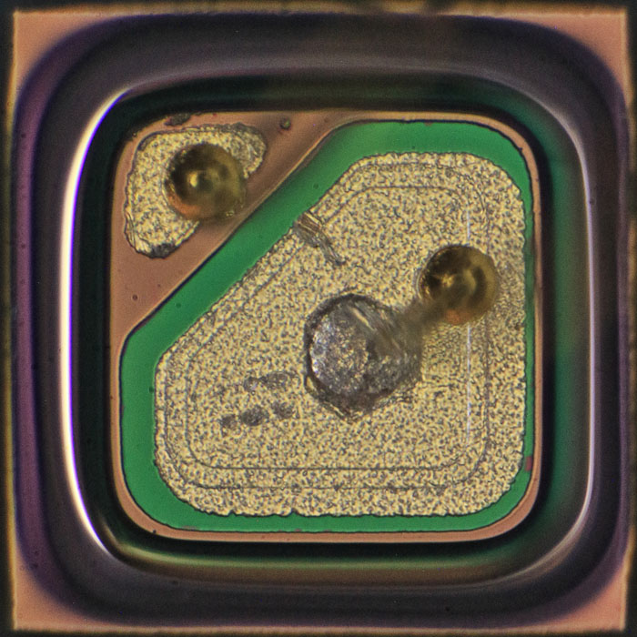
The edge length of the z-diode is 0.69mm. The design with the distinctive MESA structure is also found in the Burr-Brown DAC80 (
https://www.richis-lab.de/DAC02.htm#ZD).
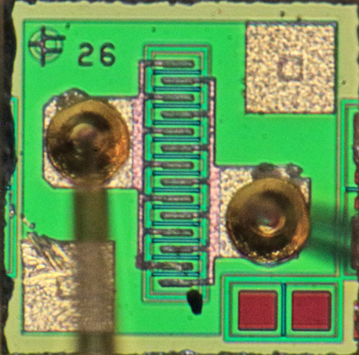
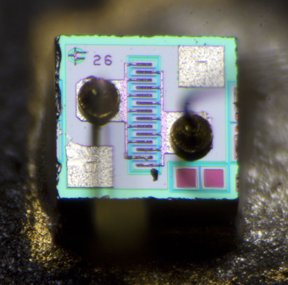
The edge length of the JFET is 0,37mm. The symbol in the upper left corner and the numbers 26 could be a hint to the manufacturer and the transistor type. Can anyone identify this part?
The bondwires feed the source and drain potential. The gate potential reaches the transistor through the substrate. The two bondpads in the corners of the dies would be alternative contact points for the gate potential. The blue elements between the source and drain areas represent the top gate electrode of the JFET. The green area is below the structures and acts as the lower gate electrode.
The test structure in the lower right corner appears to represent a large JFET.
The opamp is a National Semiconductor LM741 (
https://www.richis-lab.de/Opamp23.htm). On the right edge of the die there are the numbers 741. As described at the LM741 page the letter U after the numbers 741 is the revision of the design.
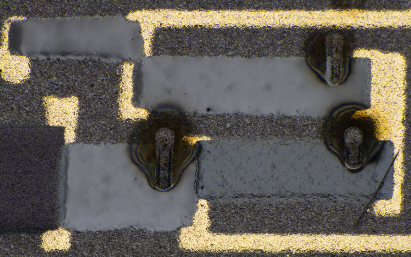
Three different resistor types appear to have been used in the compensation networks. In the bottom row, a resistor mass with a fine granular structure can be seen on the far left. This type of resistor has not been tuned. In the middle is a resistor with a smooth surface and on the right is a material with a more irregular surface. It can be clearly seen that the process of tuning has not only removed resistor mass but also heated a relatively large area of the environment.
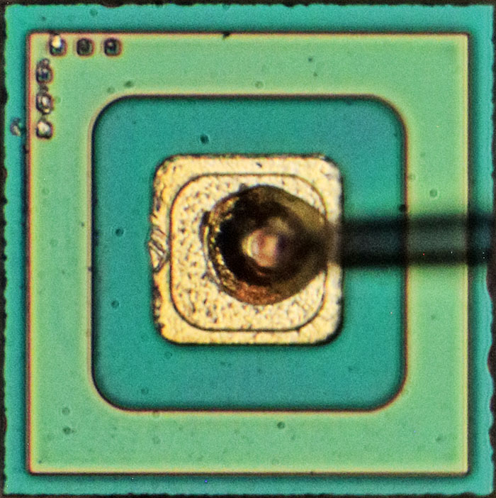
The edge length of the diode used for temperature measurement is 0,36mm. In the upper left corner there are small structures which probably allow to monitor the alignment of the masks and the quality of the manufacturing process.
The inner, darker area must be p-doped. The square that appears in the bond pad is the cutout through which the metal layer contacts the p-doped area. The light green frame must be n-doped and connected to the substrate. The substrate represents the cathode contact of the diode.
https://www.richis-lab.de/REF21.htm 


