Author Topic: More voltage references - die pictures  (Read 42660 times)

0 Members and 1 Guest are viewing this topic.

Offline NoopyTopic starter

  • Super Contributor
  • ***
  • Posts: 1726
  • Country: de
    • Richis-Lab
Re: More voltage references - die pictures
« Reply #75 on: June 26, 2022, 02:06:59 pm »
Why 'double anode', when the die has two cathodes and a single anode, shouldn't that be called a 'double cathode' diode?

Thanks for the hint! I mixed p and n!  |O
Now pictures and text are correct.
It´s too hot today...  ::)
 
The following users thanked this post: RoGeorge

Offline T3sl4co1l

  • Super Contributor
  • ***
  • Posts: 21651
  • Country: us
  • Expert, Analog Electronics, PCB Layout, EMC
    • Seven Transistor Labs
Re: More voltage references - die pictures
« Reply #76 on: June 26, 2022, 03:19:08 pm »
I wonder what hFE that has...

Is... is that still intact enough that you could get some probes on it?!  That'd be cool to see...

Hmm, ca. 200um thick... might not be enough to notice after all, think it drops off... exponentially? beyond 10s of um?

Tim
Seven Transistor Labs, LLC
Electronic design, from concept to prototype.
Bringing a project to life?  Send me a message!
 

Offline NoopyTopic starter

  • Super Contributor
  • ***
  • Posts: 1726
  • Country: de
    • Richis-Lab
Re: More voltage references - die pictures
« Reply #77 on: June 26, 2022, 03:37:22 pm »
The worst bin can be used as PNP transistors.  ;D

These parts look quite big in the pictures but contacting a 0,6mm*0,6mm*0,2mm block isn't much fun.
In addition I'm not sure if it would be possible to simply probe the n substrate and get an ohmic contact.

Offline Kleinstein

  • Super Contributor
  • ***
  • Posts: 14159
  • Country: de
Re: More voltage references - die pictures
« Reply #78 on: June 26, 2022, 03:58:21 pm »
How fast the transistor gain drops depends on the purity / carrier lifetime. With relatively pure material the diffusion length can be larger than 200 µm and carrier lifetime up to some 50 µs. For a zener diode I am afraid the substrate has relatively high doping level and this usually comes with a short carrier lifetime.

In theory one may be able to do a kind of reverse recovery test to get an idea about the carrier lifetime.  My function generator is a bit on the weak side for this, but it looks a bit like a rather fast recovery, more in the <200 ns range and not >5 µs range needed for aceptable transistor function. The 1N825 I tested is a relatively new one from microchip and not symmetric - the other direction does not show conduction at 7.5 V. So this one is not symmetric. As much as one can see from the outside the construction looks similar: a silicon die with 2 rather thick shiny metal pads on both sides.
 

Online mawyatt

  • Super Contributor
  • ***
  • Posts: 3234
  • Country: us
Re: More voltage references - die pictures
« Reply #79 on: June 26, 2022, 04:17:19 pm »
I wonder what hFE that has...

Is... is that still intact enough that you could get some probes on it?!  That'd be cool to see...

Hmm, ca. 200um thick... might not be enough to notice after all, think it drops off... exponentially? beyond 10s of um?

Tim

Remember as a kid about 65 years ago when I started getting interesting in transistors and had started the beginning of a home lab with surplus stuff. After reading a bunch of books & articles about transistors, got a couple 1N34 Germanium diodes and connected them together in an attempt to create a Germanium PNP transistor ::)  :-DD

Best,
Curiosity killed the cat, also depleted my wallet!
~Wyatt Labs by Mike~
 

Offline NoopyTopic starter

  • Super Contributor
  • ***
  • Posts: 1726
  • Country: de
    • Richis-Lab
Re: More voltage references - die pictures
« Reply #80 on: June 26, 2022, 05:10:25 pm »
The 1N825 I tested is a relatively new one from microchip and not symmetric - the other direction does not show conduction at 7.5 V. So this one is not symmetric. As much as one can see from the outside the construction looks similar: a silicon die with 2 rather thick shiny metal pads on both sides.

I have a new 1N821 here...  ;D


got a couple 1N34 Germanium diodes and connected them together in an attempt to create a Germanium PNP transistor ::)  :-DD

Sounds perfectly right!  :-+  ;D

Offline T3sl4co1l

  • Super Contributor
  • ***
  • Posts: 21651
  • Country: us
  • Expert, Analog Electronics, PCB Layout, EMC
    • Seven Transistor Labs
Re: More voltage references - die pictures
« Reply #81 on: June 26, 2022, 06:08:53 pm »
How fast the transistor gain drops depends on the purity / carrier lifetime. With relatively pure material the diffusion length can be larger than 200 µm and carrier lifetime up to some 50 µs. For a zener diode I am afraid the substrate has relatively high doping level and this usually comes with a short carrier lifetime.

Ah yeah, good point.  Guess I wouldn't know if the doping is stronger on just the diffusions, but probably has to be both (them and substrate), eh?


Remember as a kid about 65 years ago when I started getting interesting in transistors and had started the beginning of a home lab with surplus stuff. After reading a bunch of books & articles about transistors, got a couple 1N34 Germanium diodes and connected them together in an attempt to create a Germanium PNP transistor ::)  :-DD

Such tiny things!  I used a pair of 1N5404s, sadly they didn't work any better. ;D

I suppose it's....kinda dishonest, that those block diagrams are given like with ice cubes of N/P, without any mention of how they were "stacked" together, and why it has to be made in such a particular way as it does.  And why it's not cubes to begin with, for very good reason.  Well, oversimplifications being what they are...

Tim
Seven Transistor Labs, LLC
Electronic design, from concept to prototype.
Bringing a project to life?  Send me a message!
 

Offline floobydust

  • Super Contributor
  • ***
  • Posts: 6956
  • Country: ca
Re: More voltage references - die pictures
« Reply #82 on: June 26, 2022, 06:29:25 pm »
Off topic - Crystal radio experimenters playing around adding an extra cat's whisker electrode to the galena (lead sulfide PbS) crystal, discovered transistor action.
 
The following users thanked this post: ch_scr

Offline Gyro

  • Super Contributor
  • ***
  • Posts: 9473
  • Country: gb
Re: More voltage references - die pictures
« Reply #83 on: June 26, 2022, 07:49:25 pm »
This is what you're looking for guys... Complete with orignal article:  https://www.eevblog.com/forum/projects/diodes-die-pictures/msg3870872/#msg3870872
Best Regards, Chris
 

Offline NoopyTopic starter

  • Super Contributor
  • ***
  • Posts: 1726
  • Country: de
    • Richis-Lab
 
The following users thanked this post: ch_scr

Offline NoopyTopic starter

  • Super Contributor
  • ***
  • Posts: 1726
  • Country: de
    • Richis-Lab
Re: More voltage references - die pictures
« Reply #85 on: September 21, 2022, 02:20:25 pm »

Offline NoopyTopic starter

  • Super Contributor
  • ***
  • Posts: 1726
  • Country: de
    • Richis-Lab
Re: More voltage references - die pictures
« Reply #86 on: October 10, 2022, 08:16:35 am »
Some more information about the LTFLU and parts you can order from Alibaba.

Here we have the updated LTFLU page: https://www.richis-lab.de/REF04.htm

And here we have the LTFLU (Alibaba) page: https://www.richis-lab.de/REF25.htm

Here we have the "englisch version": https://www.eevblog.com/forum/metrology/the-ltflu-(aka-sza263)-reference-zener-diode-circuit/msg4456426/#msg4456426
 
The following users thanked this post: iMo, arcnet

Offline NoopyTopic starter

  • Super Contributor
  • ***
  • Posts: 1726
  • Country: de
    • Richis-Lab
Re: More voltage references - die pictures
« Reply #87 on: October 24, 2022, 08:05:41 pm »


We had this old 1N829A: https://www.richis-lab.de/REF22.htm
Now here we have a 1N821 built by Microsemi (now owned by Microchip Technology) which I bought this year.
The 1N821 is the worst bin of the family with a temperature coefficient of 0,01%/K.


The die can be seen in the center of the glass package. The picture improves when you carefully crack the case open. The red areas are treated to reliably bond with the glass. Round metal elements are applied to it, each of which has a kind of plinth. The die in the center is 0,23mm thick.


Here the body is already disassembled. The elevated placement due to the plinth is clearly visible.


The contacts are more complex than one would expect. There is a very smooth layer on both contacts, reminiscent of a silicon surface. A round structure can be seen around the contact area.


The silicon block in the center has round contact areas on both sides that match the contacts. According to the optical appearance, the red area contains the initial doping of the substrate. The green region most likely contains the inverse doping to it, creating a diode structure. The two diodes on the two sides are connected via the substrate, resulting in the desired series connection of a zener and a "normal diode".

The contacts are apparently just used for contacting. Why the relatively complex surface was built there remains unclear.  :-//


https://www.richis-lab.de/REF26.htm

 :-/O
 
The following users thanked this post: SeanB, Andreas, BU508A, RoGeorge

Offline NoopyTopic starter

  • Super Contributor
  • ***
  • Posts: 1726
  • Country: de
    • Richis-Lab
Re: More voltage references - die pictures
« Reply #88 on: November 15, 2022, 12:44:19 pm »


Finally, a TL431!  8)

The TL431 is a very widely used voltage reference developed by Texas Instruments. It could be that the TL431 and its variants have been sold even more often than the famous NE555. A typical application is the reference voltage generation in power supplies. The integrated amplifier makes it possible to get by with very few components.

The TL431 shown here has been built 1986. The I at the end of the designation stands for the bin with the larger temperature drift of typically 14mV. There are also variants available that carry another letter after this one and offer different initial tolerances. The best grade has an accuracy of 0,2% and typically drifts 6mV over the operating temperature range.


The TL431 is a shunt regulator. The datasheet shows typical applications. If you connect the REF with the cathode, the device works similar to a zener diode, which explains the symbol of the TL431. The reference voltage then is 2,5V. With a voltage divider at the REF input one can set any reference voltage up to 36V.


The block diagram in the datasheet shows the basic structure of the TL431. Between cathode and anode is the shunt regulator, which is protected from negative voltages by a freewheeling diode. An operational amplifier controls the shunt transistor, by comparing the voltage at the REF input with an internal reference voltage.


In addition to the block diagram, the datasheet shows a circuit diagram, which I have colored and provided with some additional designators.

The core of the circuit is a bandgap reference, which roughly corresponds to the reference in the TDB7805 (https://www.richis-lab.de/voltageregulator05.htm). The goal of a bandgap reference is to compensate the negative temperature coefficient of the forward voltage of a pn junction with a positive temperature coefficient. To do this one uses the temperature voltage that is included in a pn junction too. Its small positive temperature coefficient is usually overcompensated by the larger negative temperature coefficient of the forward voltage.

The red area generates the voltage with the positive temperature coefficient. For this purpose, the transistors T3/T4, which work as current mirrors, are designed with different sizes. This would result in different currents in the two branches. The 800Ω resistor ensures equal currents nevertheless. In the T3/T4/800Ω loop, the negative temperature coefficients of the two forward voltages cancel each other out. Across the 800Ω resistor you see the difference of the two forward voltages, (caused by the different current densities). This voltage still contains the positive temperature coefficient, which results from the temperature voltage of the pn junctions. The 800Ω resistor generates a current with a positive temperature coefficient, which subsequently flows through the 7,2kΩ resistor. The voltage drop across this resistor then represents one part of the reference voltage. The 7,2kΩ/800Ω resistor ratio amplifies the small positive temperature coefficient and thus defines its share of the reference voltage.

The base-emitter path of transistor T5 (dark red) provides the negative temperature coefficient of the reference voltage and in addition represents the control output. If the voltage at the input of the bandgap reference increases, the transistor T5 conducts more current. The 3,28kΩ resistor in the supply line to the bandgap reference is used for biasing (purple). The 20pF capacitor limits the bandwidth and thus prevents oscillations.

The cyan area is the interface between the bandgap reference and the output stage. Transistor T6 forms a cascode circuit with T5. Thus T5 is protected from potential changes at its collector. The current mirror T7/T8 copies the current from T5 towards the output stage and controls it in such a way that the voltage between cathode and anode of the TL431 is adjusted to the desired level. The transistor T9 (green) is a current sink for biasing T8.

The output stage (blue) is built with two transistors in a Darlington circuit. Another 20pF capacitor limits the bandwidth here as well. The diode D2 protects the circuit against negative voltages. The necessity of D1 remains unclear.

Transistor T1 (yellow) reduces the current that the TL431 draws from the REF input, so that any external voltage divider is less loaded. Transistor T2 reduces the driver current of the output stage if there is a fast voltage dip at the input.


The dimensions of the die are 1,2mm x 1,0mm. TL431 is shown in the lower area.

There are no fuses or other possibilities to tune the circuit. There is just a testpad at the cathode potential.


On the die the bandgap reference is arranged on the left side. The transistor T4 is divided into two transistors and integrated around T3. This creates the necessary area ratio and guarantees that the temperature of the two transistors is as equal as possible.

The output stage is located on the right side. The largest element is the power transistor at the right edge. Not directly visible are the diode D1 and D2. Apparently these are just the parasitic diodes that form between the p-doped substrate and the n-doped collector region of each NPN transistor, in this case at T9 and T11.


At the left edge of the die the resistors with the values 2,4kΩ, 7,2kΩ, 800Ω and 3,28kΩ are represented by many small resistor elements. For better understanding, these are colored differently here. It is a mixture of series and parallel connection. The network most likely has two tasks. On the one hand, the interconnection ensures that the temperatures are as equal as possible, thus reducing temperature drifts. On the other hand, the interconnection and thus the resistance values can be changed by modifying the metal layer. On some resistors the contacts are very wide, so that only the vias can be moved for smaller adjustments.


The two 20pF capacitors are very different. This is due to the fact that the capacitance located at the output transistor T10/T11 (left) is a classic capacitor, while the capacitance in the bandgap reference (right) is represented by a pn structure.

In the classical capacitor, the electrodes are the metal surface and the underlying n-doped surface. Between them there is usually an oxide layer as thin as possible in order to represent a high capacitance per unit area.

The pn structure takes advantage of the fact that its junctions are very thin, which enables a significantly higher capacitance per unit area. However, the voltage strengths of the junction must be taken into account, which is why this type of capacitor cannot be used everywhere.


In detail you can see the structure of the pn-capacitor. When assigning the areas and structures, a comparison with a normal NPN transistor (here top left) is useful.

The upper potential is connected to the base area which appears red. The lower potential contacts not only emitter areas, but also the collector area. Thus, both the base-emitter junction and the base-collector junction serve as capacitance. Both junction layers must, of course, be operated in the reverse direction for this purpose. The base-emitter junction defines the maximum permissible voltage, which is usually in the low single-digit volt range, depending on the doping.

It is nice to see that it is not a full area emitter, but three individual areas. By adjusting the areas or cutting off one area completely, one can change the effective capacitance.

The structures in the collector area belong to the low impedance collector feed line ("buried collector"). It remains questionable which background the edges in the base area have. The structure is located in the area where the base and emitter layers lie on top of each other, but it leaves out the contact areas.  :-//


https://www.richis-lab.de/REF27.htm

 :-/O
 
The following users thanked this post: SeanB, Andreas, Kean, doktor pyta, Jim Narem, BU508A, RoGeorge, ch_scr, iMo, eplpwr, DH7DN

Offline NoopyTopic starter

  • Super Contributor
  • ***
  • Posts: 1726
  • Country: de
    • Richis-Lab
Re: More voltage references - die pictures
« Reply #89 on: November 28, 2022, 06:15:26 pm »


The AD580 from Analog Devices is a 2,5V voltage reference in a TO-52 package. There are a total of seven variants with slightly different specifications. The first letter after the type designation identifies the variant. The letters J, K, L, M keep their specifications in an operating temperature range from 0°C to 70°C. The specifications of the variants S, T, U are slightly worse, but refer to an operating temperature range from -55°C to 125°C.

The best bin AD580M guarantees an initial error of +/-10mV max. The temperature drift is 10ppm/°C max. In addition, there is a long-term drift of 250µV. The current consumption is just 1.5mA.


The datasheet of the AD580 contains a schematic which corresponds to the schematic in the patent US3887863A and thus is the same as in the AD1403 (https://www.richis-lab.de/REF16.htm). Only the resistor marked UP in the patent specification is missing here. On the die, however, it can be seen that the resistor is present in the AD580 too. The circuit was analyzed in more detail in the context of the AD1403.


The output of the voltage reference is connected to the die with two bondwires.


The datasheet contains a picture of the metal layer of the die. Since the AD580 can be purchased as bare die, there is an extra note that both eout bondpads must be connected to the output. The control loop of the voltage reference is closed via these bondpads.


The die is surprisingly high.


The design dates back to 1990 and it seems that the AD580 is an updated version of the AD1403.

In the overview, many elements are clearly visible. The more powerful transistors are integrated on the left side, while the bandgap reference transistors are on the far right. As shown in the schematic, there are two transistors with a size ratio of 8:1. The larger transistor is divided into two elements and surrounds the smaller transistor, so that all structures have as equal temperatures as possible.

The resistor at the lower edge was adjusted with a laser and allows to adjust the output voltage. The resistors on the right edge are used to adjust the temperature drift. For this purpose two testpads contact the bandgap reference directly.

In the upper right corner there is a test structure, which is typical for laser tuned circuits. The structure is used to adjust the tuning process. Next to it, a 1 has been written in a square. This could be the documentation of a quality level or the number allows tracing the alignment process.


https://www.richis-lab.de/REF28.htm

 :-/O
 
The following users thanked this post: SeanB, Mickle T., Andreas, BU508A, RoGeorge, ramon, ch_scr, iMo, eplpwr, arcnet

Offline NoopyTopic starter

  • Super Contributor
  • ***
  • Posts: 1726
  • Country: de
    • Richis-Lab
Re: More voltage references - die pictures
« Reply #90 on: March 20, 2023, 07:01:54 am »
Pictures from inside the ADR1001 can be found here in the ADR1001 thread:

https://www.eevblog.com/forum/metrology/adr1001-ovenized-voltage-reference-system/msg4767737/#msg4767737

And of course on my website:

https://www.richis-lab.de/REF29.htm

 :-/O
 
The following users thanked this post: mycroft, Gyro, BU508A, RoGeorge, bsw_m, alm, MiDi, ch_scr, maat, iMo, DH7DN

Offline NoopyTopic starter

  • Super Contributor
  • ***
  • Posts: 1726
  • Country: de
    • Richis-Lab
Re: More voltage references - die pictures
« Reply #91 on: May 17, 2023, 06:44:16 pm »


The REF3033 is a voltage reference built by Texas Instruments. It outputs a voltage of 3,3V. Other variants produce the common 1,25V 2,5V and 3,0V voltage levels (REF3012, REF3025 and REF3030). Additionally, 2,048V and 4,096V are available, values adjusted to integer binary division factors (REF3020 and REF3040).

The initial accuracy of the voltage is given in the datasheet as +/-0,2%. Between 0°C and 70°C the temperature drift is 50ppm/°C max. Between 0,1Hz and 10Hz you have to expect a noise voltage of up to 45µVpp. The aging drift is given as 24ppm for the first 1000 hours and 15ppm for the second 1000 hours.

Current consumption is typically just 42µA. The device can deliver up to 25mA. The input voltage only needs to be 300mV higher at this operating point. Without load even only 1mV is specified as typical value.


According to the datasheet, the REF3033 is based on a CMOS process. The schematic above is taken from the datasheet and shows that the output voltage is based on a bandgap reference, as it is described in more detail for example in the AD1403 (https://www.richis-lab.de/REF16.htm). Interesting is the rotated arrangement of the bipolar transistors. Usually, the emitters are connected to GND via their emitter resistors. This is not the case in the REF3033. Nevertheless the working principle is very similar. The voltage with the necessary positive temperature coefficient drops at resistor R1.


On the die there is a protective layer with some openings. Most likely, this is a polyimide layer.


The dimensions of the die are 1,4mm x 0,7mm.


In the upper right corner there is a very wide bondpad. The beveled corners are an indication that this is pin 1, which supplies the device. This is matched by the massive connection to the wide parallel supply lines. In the lower left corner, another wide bondpad gets the ground potential. The wide bondpads seem to be a hold-off to connect the supply and the reference potential with two bondwires.

In the upper left corner is the output and another bondpad. The output can be recognized by its massive connection to a larger structure. The upper bondpad is almost certainly a sense input, reading back the output voltage directly at the pin. The not-contacted bondpad in the lower right corner is most likely used for an adjustment of the device.


The design apparently dates back to 2001. The first revision of the datasheet dates back to 2002.


On the left edge, the strings ICC02978 and ICC02974 are integrated. Judging by the colors, the characters are "written" with the mask for the metal layer and the mask for the bondpads. Why there are two different strings remains unclear.


A little further in the center, the revisions of six masks can be seen. The characters OP3 cannot be assigned with absolute certainty. It is quite possible that variants of the metal layer are shown here, representing the different output voltages.


Next to the Texas Instruments logo, there are eight electrically isolated squares that were partly cut with a laser. These squares, to which letters are assigned, are known from Burr-Brown (see for example the OPA627: https://www.richis-lab.de/Opamp22.htm).


In the right area at the lower edge, there are two bright stripes that are presumably used to align the laser. Ten resistor strips are integrated to the left. You can't see any traces of an alignment, but the opening in the polyimide shows that this area is used for alignment.


In the upper left area of the die two more strips with adjustable resistors are integrated.


The structures are very small. On closer inspection, however, you can see that the large purple areas consist of very many resistor strips that are contacted very differently at the sides. The brighter area in the upper region could be a capacitor.

There is every indication that the right area contains much of the basic bandgap reference. The regular structures in the two larger rectangles could contain the bipolar transistors. The central arrangement would suggest this. The very complex structure of the resistors could be used to compensate for parasitic effects and drifts. The adjustable resistors at the lower edge are then used to adjust the strength of the positive temperature coefficient.


The left area of the die most likely contains the differential amplifier of the bandgap reference and of course the regulator transistor. The relatively large output transistor is clearly visible between the bondpads.

The adjustable resistors at the top edge are most likely used to adjust the output voltage. It can be assumed that the rough adjustment of the output voltage for the different variants is done by different structures in the metal layer. The final adjustment is then made via the laser alignment.


https://www.richis-lab.de/REF30.htm

 :-/O
 
The following users thanked this post: SeanB, Mickle T., Andreas, Jim Narem, BU508A, RoGeorge, alm, ch_scr, eplpwr, mawyatt

Offline BU508A

  • Super Contributor
  • ***
  • Posts: 4522
  • Country: de
  • Per aspera ad astra
Re: More voltage references - die pictures
« Reply #92 on: May 18, 2023, 07:20:11 am »
How cool is that?   :D  8)

Thank you Noopy, for going through all those efforts, much appreciated!  :-+ :-+
“Chaos is found in greatest abundance wherever order is being sought. It always defeats order, because it is better organized.”            - Terry Pratchett -
 
The following users thanked this post: Noopy

Offline NoopyTopic starter

  • Super Contributor
  • ***
  • Posts: 1726
  • Country: de
    • Richis-Lab
Re: More voltage references - die pictures
« Reply #93 on: June 29, 2023, 08:11:21 pm »


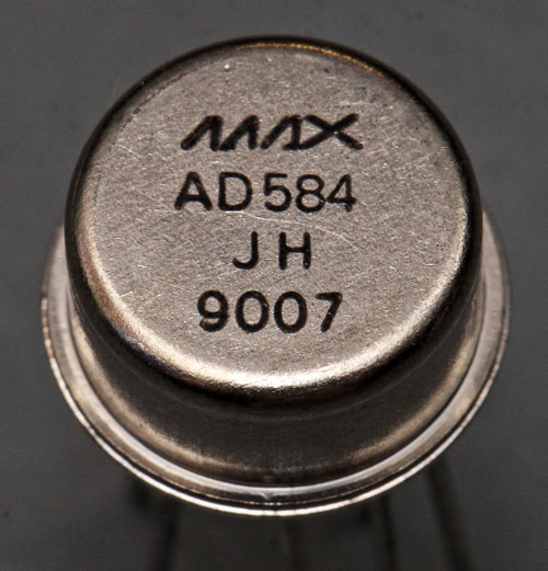
As the name implies, the AD584 reference voltage source was originally developed by Analog Devices. Maxim had its own variant on offer, which can be seen here. The index J is the worst of three bins. The best bin L offers an accuracy of +/-2,5mV (on the 2,5V rail). The temperature drift is typically given as 3ppm/°C. In addition, there is a long-term drift of 25ppm/1000h. The noise voltage is 50µVpp (0,1-10Hz). The output delivers up to 10mA. A strobe input can be used to deactivate the AD584, which reduces the current consumption from 750µA to 100µA.


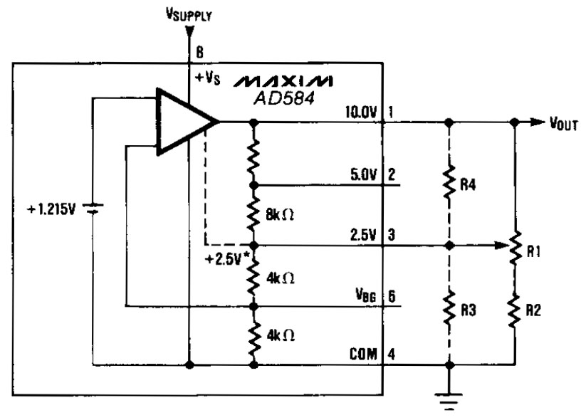
The AD584 offers four outputs: 10V, 5V, 2,5V and the bandgap voltage, which usually is 1,215V. The datasheet shows how to adjust the reference voltage to other values with additional resistors.


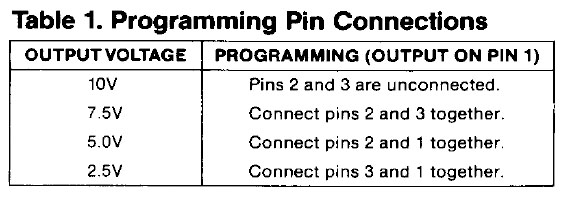
Depending on which output voltage you want to use, you can bridge different pins and thus adjust the internal voltage divider. In such a connection, the respective output offers the specified load capacity. If you use an external buffer, you can work without bridges and also access several of the output voltages.


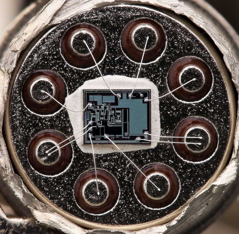
In the housing it can be seen that both the 10V reference potential and the reference potential are connected with two bondwires. Here, the connection has not simply been reinforced. On the die, the bondwires each contact different potentials.


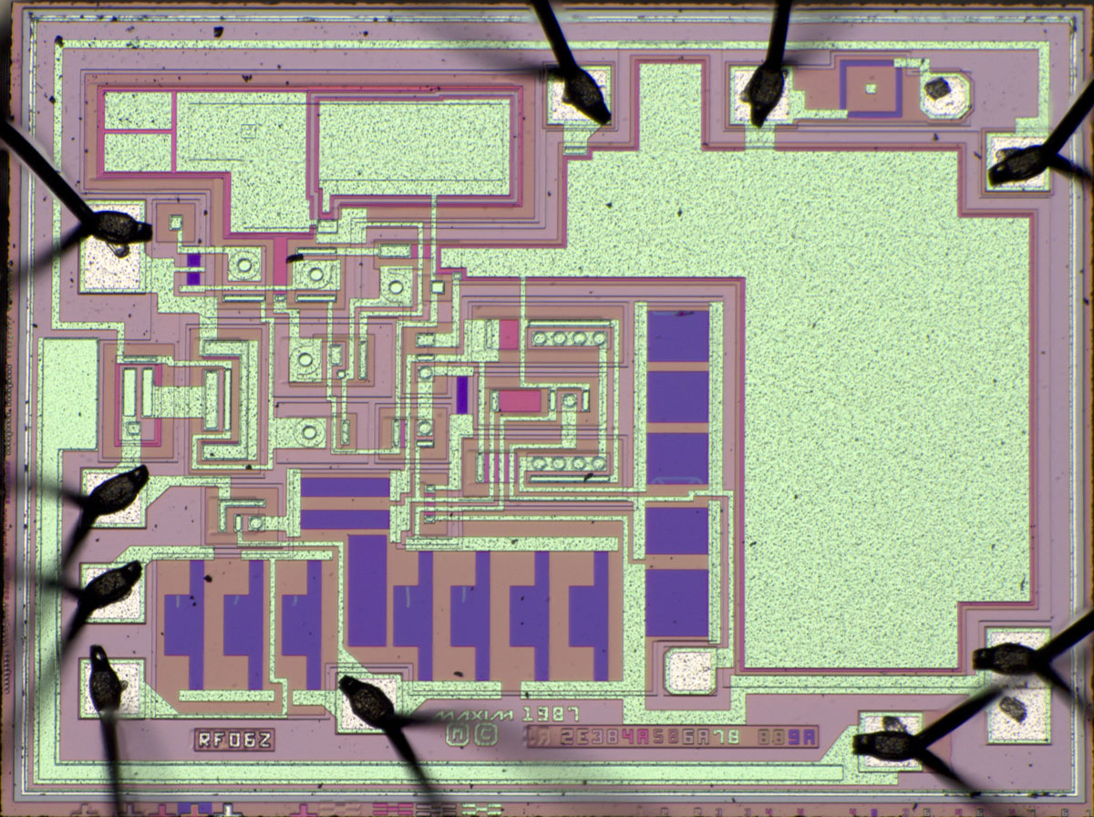
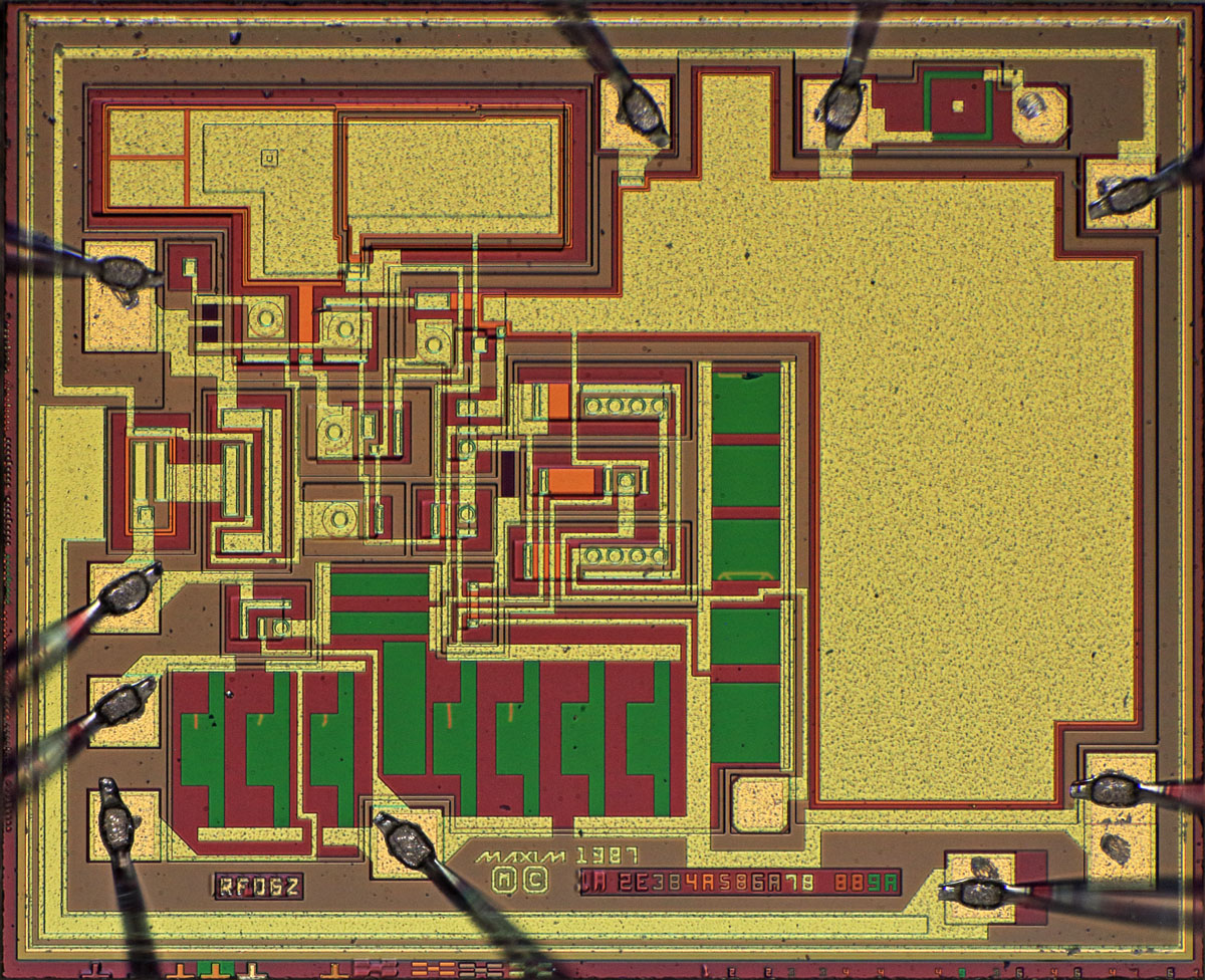
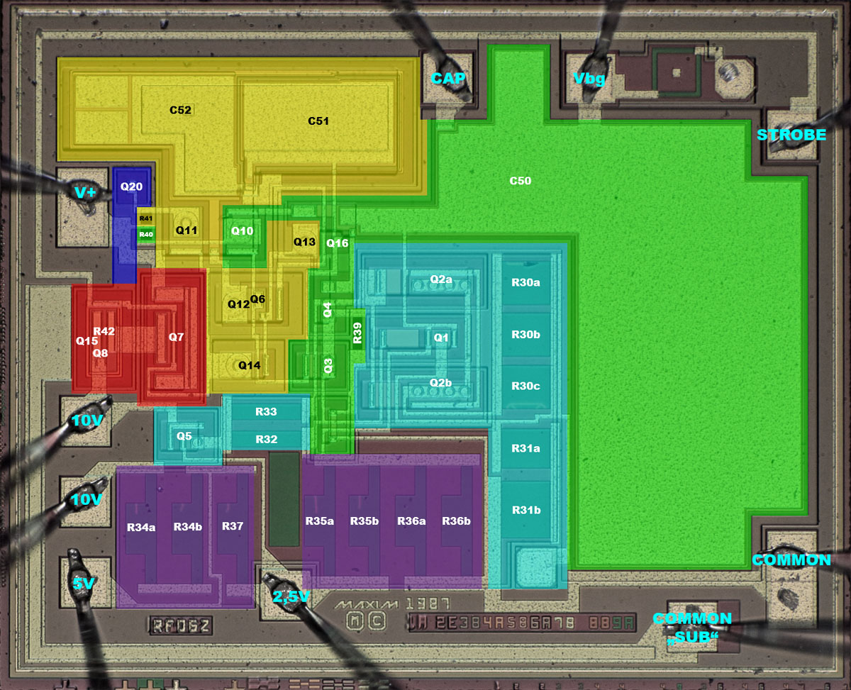
The dimensions of the die are 2,2mm x 1,8mm.


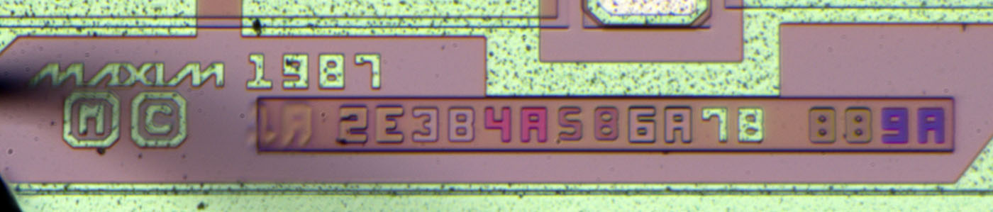
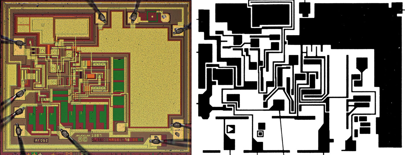
The design is obviously from Maxim and dates back to 1987.

Nine masks are depicted on the lower edge of the die. Many can be assigned to their function. 1A depicts the low-lying collector feed line. 2E creates the isolated areas. 4A represents a strong n-doping. Since the metal layer is preceded by mask 5B, it seems likely that 4A generates so-called sinkers, the connection between the low-lying n-dotations and the surface. 5B then generates the emitter regions. 6A creates openings in the silicon oxide through which the metal layer contacts the active elements. 7B then structures the metal layer. 9A obviously serves to define the shape of the adjustable resistors. 8B could be the mask that opens the passivation layer in the bond areas.

Some masks have been revised once. The mask for the isolated wells (2E), on the other hand, has been revised four times.


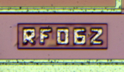
RF06Z seems to be the internal designation of the AD584. One can guess that at least a similar string is shown in the lower layers.


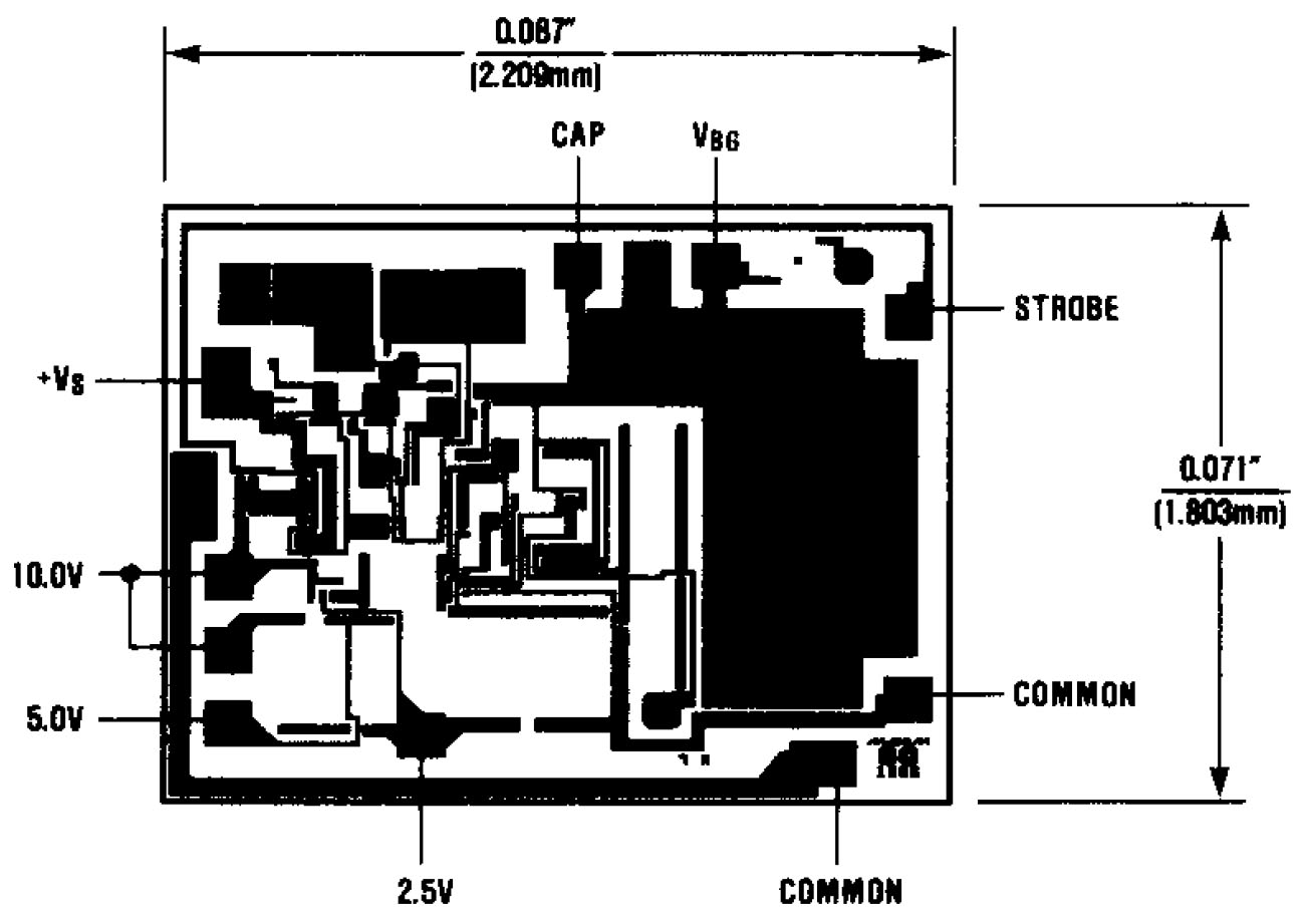
The Maxim datasheet for the AD584 contains an illustration of the metal layer that matches the present die very well. The only noticeable difference is in the bottom right corner, where the bondpad for the reference potential has been extended on the present die. The Maxim logo with the copyright had to be moved to the left accordingly.


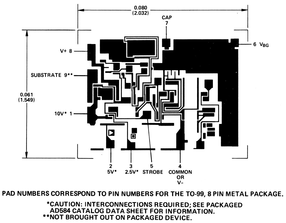
In the Analog Devices Data-Acquisition Databook from 1982, the metal layer of the Analog Devices AD584 is shown. This AD584 is slightly smaller than the Maxim model: 2,03mm x 1,55mm versus 2,2mm x 1,8mm.

You can see that the arrangement of the areas on the die is roughly the same. However, they are clearly two different designs.


In the middle of the die, you immediately notice the typical bandgap structure, where a large transistor surrounds a small transistor. The ratio of the transistors here is 8:1. The working principle of a bandgap reference voltage source is described in more detail in the context of the AD1403 (https://www.richis-lab.de/REF16.htm).

In the right area there are adjustable resistors. The traces of the adjustment are clearly visible. It is interesting that not only a simple cut was made at the lower resistor. An area was cut off whose ends describe a kind of triangle.


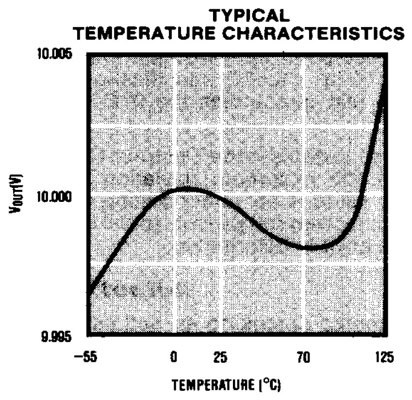
A bandgap reference compensates the negative temperature coefficient of the forward voltage of a pn junction with the positive temperature coefficient of the thermoelectric voltage of a pn junction. The datasheet of the AD584 shows the temperature variation of the output voltage and thus also that the compensation of the temperature coefficients is not perfect.


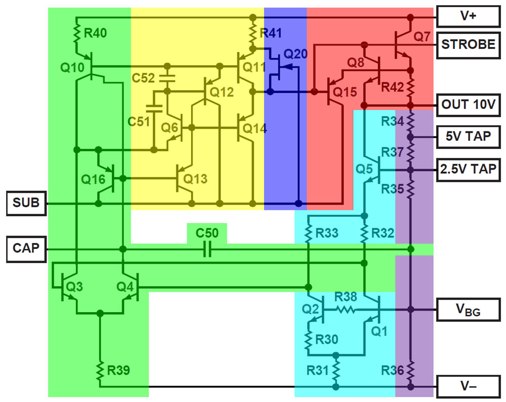
The datasheet from Analog Devices contains a complete circuit diagram for the AD584. As will become apparent, the circuit corresponds almost exactly to Maxim's circuit.

The core of the typical bandgap cell (cyan) is formed by the transistors Q1 and Q2. Q5 represents the associated current source. The 2,5V reference voltage is used to control this current source. This is also the reason why the datasheet points out that this node must not be trimmed more than 100mV.

The two branches of the bandgap reference are connected to a differential amplifier (green). The differential amplifier is supplied by Q10, which descripe two current sources. C50 reduces the noise of the reference output. For this reason, the package provides the CAP pin. Up to 100nF can be added externally between CAP and Vbg to further reduce noise.

The differential amplifier is followed by a somewhat unusual amplifier stage (yellow), at whose output is the push-pull stage Q11/Q14. C51 and C52 stabilise the circuit. It is interesting that this section is directly connected to the substrate. In principle, the substrate and the reference potential V- have the same potential, but the separation reduces the danger of disturbing feedback effects from the output driver to the reference voltage source.

Q20 (blue) ensures a safe start-up of the circuit. Q7 forms the output driver of the output stage (red). The output can be switched off with the strobe input. This pin is directly connected to the base of the output stage transistor. Q8 and R42 form an overcurrent protection. Transistor Q15 is a way of diverting the output current from Q7, which improves the control behaviour.

Below the 10V output is a resistor divider (purple) that maps the different output voltages.


The control loop closes at the base of transistor Q1. At this point, the bandgap voltage is set at which the temperature coefficient becomes minimal. Since the control loop closes across the voltage divider, you can load the taps without changing the voltages. Of course, these taps are not as powerful as the 10V output. For this reason, you have to bridge outputs as described above if you want to fully load the lower output voltages.


All the elements of the Analog Devices circuit diagram can be found on the die. Only resistor R38 is missing. The base current of the transistors Q1/Q2 flows through the voltage divider at the output. It varies with the amplification factor and thus also with the temperature, which creates an additional temperature drift. The influence can be compensated by a resistor between the transistors. Alternatively, the voltage divider can be designed with as low an resistance as possible. Since the output is relatively powerful, the voltage divider could probably be chosen with sufficiently low resistance and thus do without the base resistor.

In the upper right corner of the die is the familiar square structure that can be used to set the adjustment process. The resistors R30 and R31, which define the temperature coefficient of the reference voltage, are adjusted. A testpad under R31 facilitates the adjustment. Resistors R34-R37, which define the value of the individual reference voltages, are also adjusted. The resistor R39 in the current sink of the differential amplifier and the collector resistors R23/R33 are made of the same material, but the geometries are much smaller. Presumably, the material was not chosen for balancing, but for other reasons.


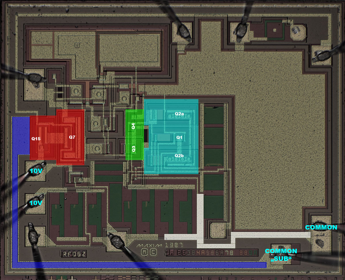
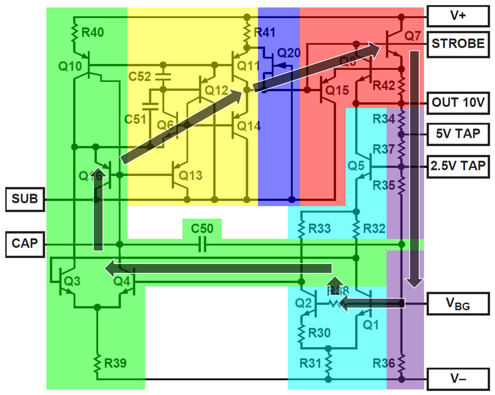
The output stage (red) and the critical elements of the bandgap reference (green/cyan) are arranged in such a way that the heat dissipation of the output stage affects the two paths of the bandgap reference as equally as possible.

The upper of the two 10V bondpads is connected to the output stage. From the 10V pin, the second bondwire then leads to the voltage divider on the die. This also compensates for the voltage drop across the bondwires. The reference potential is connected to the substrate over the entire lower edge and half of the left edge (blue). Next to the output stage, there is also a large-area contact to the substrate. The bandgap reference is connected to the reference potential via the second bondwire so that it is not influenced by load currents.


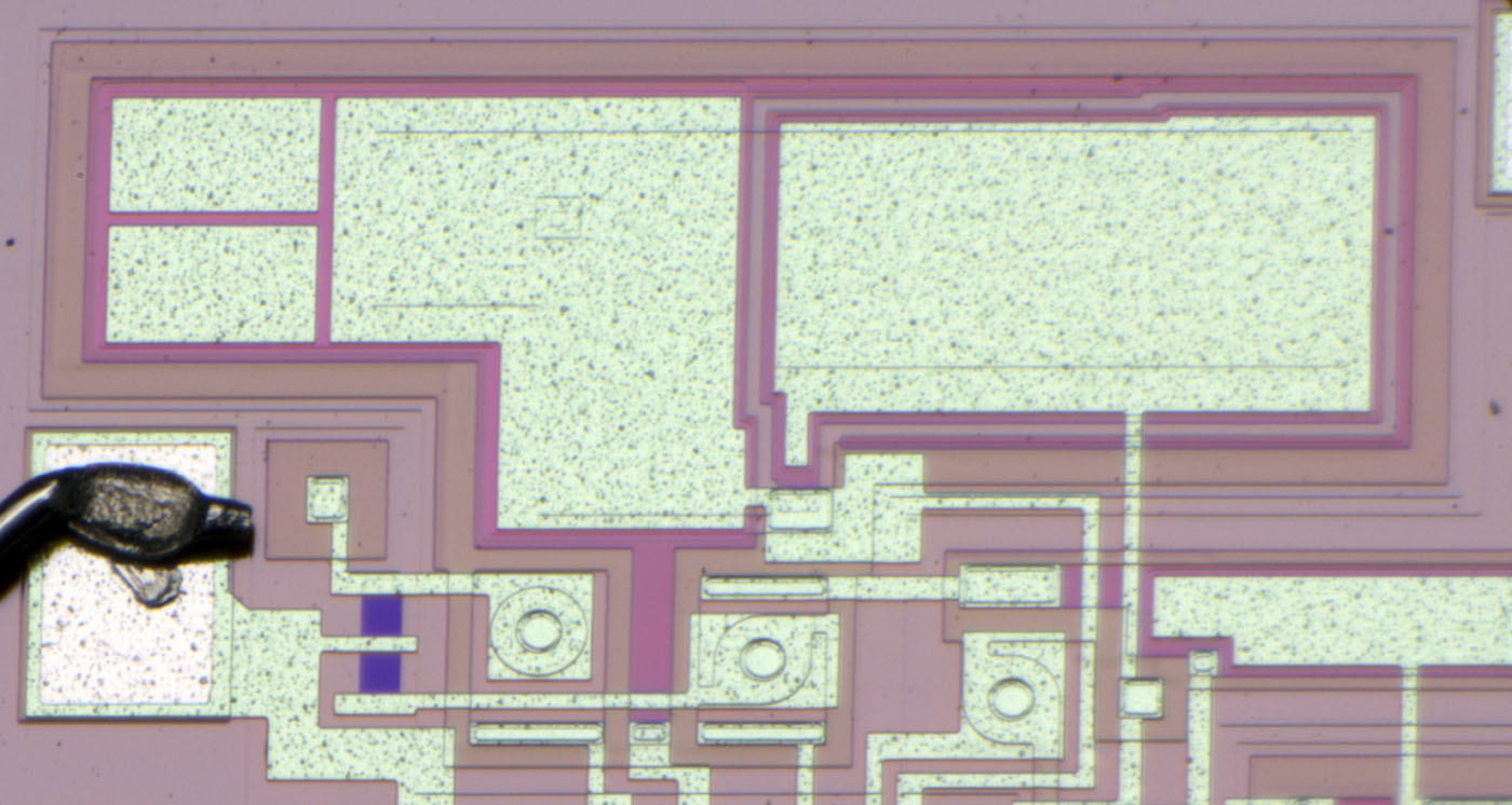
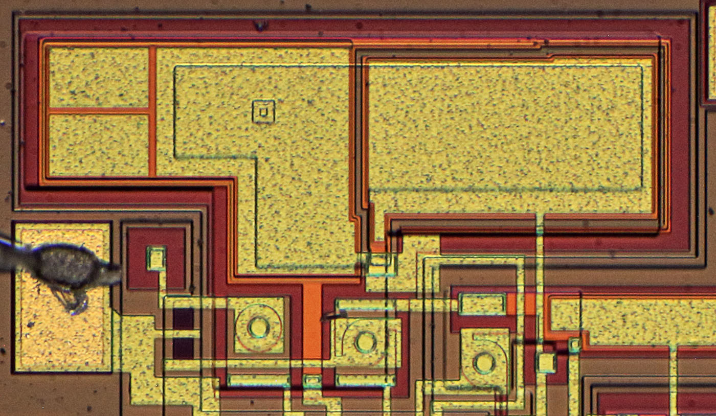
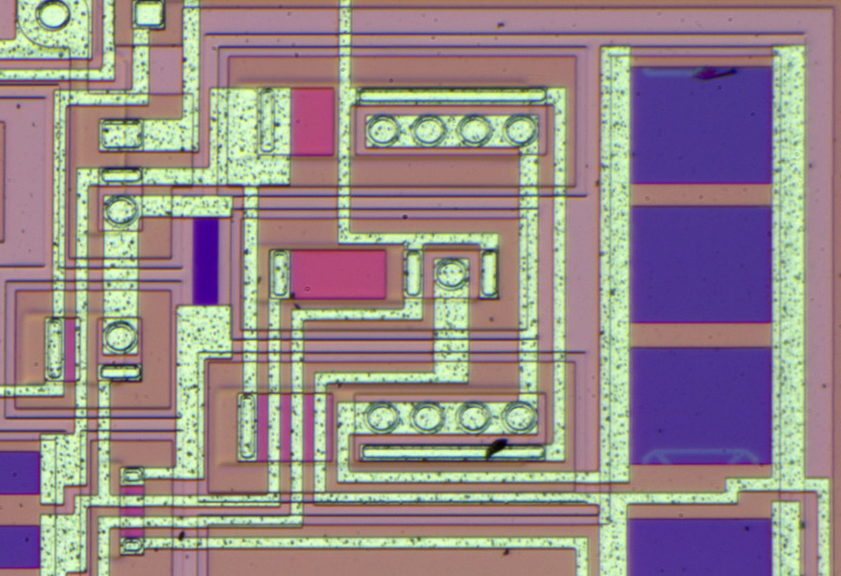
Capacitor C50 occupies almost half of the silicon area. In contrast, the capacitors C52 (left) and C51 (right) are much smaller. C51 is a classic capacitor, while C52 additionally uses the capacitance of the base-emitter junction. This can be seen in the contact window, which is visible in the metal layer. In the left area, the capacitance can be varied with two additional metal areas so that one can set an optimum between control speed and stability.


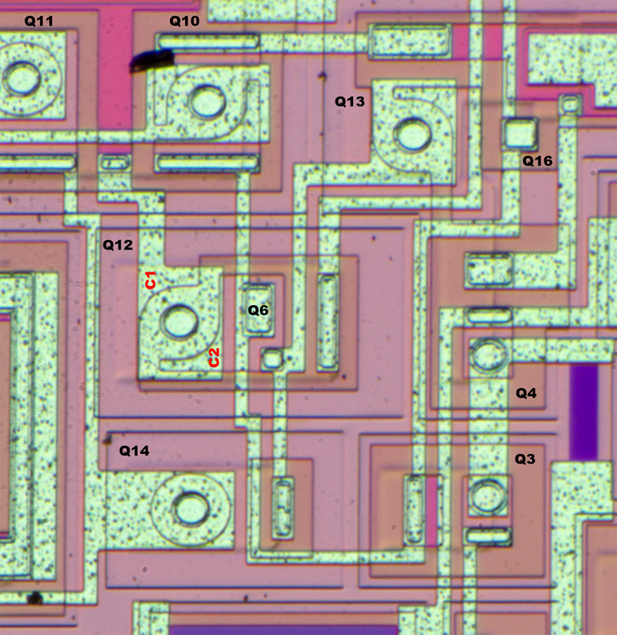
Usually, transistors are located in an n-doped well enclosed by p-doped regions. As long as the substrate has the most negative potential of the circuit, the wells are electrically isolated. This can be seen well in transistors Q3 and Q4, where the orange material represents the n-doping surrounded by the p-doping, which appears light pink. The slightly more prominent structures are p-doped frames that extend to the substrate.

As shown in the schematic, some transistors are directly connected to the substrate. This can be seen clearly in the case of transistor Q14, where the orange n-doping has only been introduced at the base contact. The collector is the p-doping surrounding all sides, which is directly connected to the substrate via the frame structure.

The transistor Q12 has two collectors. While C1 is directly connected to the substrate, as in Q14, C2 and its surroundings are somewhat more obscure. In the centre of the large metal surface is the circular, p-doped emitter, as usual for a PNP transistor. The ring around this circle is the n-doped base. The base area has been extended to the right and contains the p-doped collector C2, which is isolated from the substrate and is contacted in the lower right corner. In this p-doped collector area, an n-doping has again been introduced so that the NPN transistor Q6 can form there.

The PNP transistor Q16 is just as difficult to recognise. Here, the metal layer contacts a square, p-doped area that is completely covered by the metal layer. This area is located in an n-doped area, so that a substrate transistor is formed.


https://www.richis-lab.de/REF31.htm

 :-/O
 
The following users thanked this post: SeanB, Mickle T., Andreas, Jim Narem, BU508A, RoGeorge, ramon, alm, ch_scr, iMo, eplpwr

Online AnalogTodd

  • Regular Contributor
  • *
  • Posts: 85
  • Country: us
Re: More voltage references - die pictures
« Reply #94 on: June 29, 2023, 09:47:35 pm »

Interesting bits to take into consideration: this is a very basic bipolar process with the addition of two layers, the rich N-doping to get low resistance connections to the buried N-doping and a deposited resistor (likely sichrome) layer. Layer 1 is the buried N-doping and is not perfectly aligned in the mask revisions box because the shadow that appears on the surface of the die is offset from the actual location of the buried N-doping due to the crystal structure of the wafer and the epi growth process. Layer 2 is P-type isolation to define tubs for individual transistors and resistors, Layer 3 is the shallow P-base used for NPN transistor bases and lateral PNP emitter and collector diffusions, layer 4 is the deep N connection to the buried N, layer 5 is the shallow N+ for NPN emitters (and sometimes connection to layer 4). Layer 6 makes contact to the silicon, layer 7 is metallization, layer 8 is oxide/nitride passivation, and layer 9 is the deposited resistor layer.

The deposited resistor layer has some benefits such as being very resistant to mechanical stress on the die. The 8:1 transistor pair of Q1 and Q2 is centered in the die for avoiding mechanical stress as well. What is quite noticeable on the deposited resistors is the thin lines etched into a number of them. The shape of the resistors and those lines are hallmarks of laser trimming of the resistor values. Resistors R34, R35, and R37 are trimmed to match R36 and give precise output voltages. Trims are also seen on R30 and R31 to get the bandgap voltage as close to the magic voltage that provides a flat output across temperature. The targets to align the laser to the resistor positions are not seen on the die, they are likely in part of the scribe that was lost during wafer saw.
Lived in the home of the gurus for many years.
 
The following users thanked this post: RoGeorge, ramon, alm, razvan784

Offline NoopyTopic starter

  • Super Contributor
  • ***
  • Posts: 1726
  • Country: de
    • Richis-Lab
Re: More voltage references - die pictures
« Reply #95 on: June 30, 2023, 02:58:48 am »
The targets to align the laser to the resistor positions are not seen on the die, they are likely in part of the scribe that was lost during wafer saw.

As far as I know the rectangle in the upper right corner is used to align the laser. Perhaps there is another structure in the scribe line.

Online magic

  • Super Contributor
  • ***
  • Posts: 6748
  • Country: pl
Re: More voltage references - die pictures
« Reply #96 on: June 30, 2023, 08:26:34 am »
The resistor square in the top right corner looks like a test structure included to measure resistance of the thin film layer.

Analog Devices die revision D is on zeptobars.
R38 is also not included.
R31 includes a segment made of diffused resistor, which according to Brokaw was intended for curvature correction. Not sure why Maxim doesn't have it.

The differential amplifier is followed by a somewhat unusual amplifier stage (yellow), at whose output is the push-pull stage Q11/Q14. C51 and C52 stabilise the circuit.
The output stage is driven from Q4 collector by a straightforward darlington emitter follower Q13,Q14.
Q11 contribution to output stage control seems negligible due to its collector having much higher output impedance than Q14 emitter. That being, it is a mirror of Q3 collector current so it works in phase with Q4 and Q14.
Q6 allows Q3 to drive the PNP current mirror while having constant collector voltage roughly equal to Q4, this improves PSRR at Q3/Q4 and more importantly at Q10 (lousy lateral PNP with low Early voltage).
Current injected into Q3 by Q6 is the base current of Q12, while Q4 receives the base current of Q13.
The weird splitting of Q12 ensures that these currents are equal (Q12 passes base currents of Q10+Q11, Q13 half of the former plus base current of Q14).
« Last Edit: June 30, 2023, 09:25:24 am by magic »
 
The following users thanked this post: Noopy

Online AnalogTodd

  • Regular Contributor
  • *
  • Posts: 85
  • Country: us
Re: More voltage references - die pictures
« Reply #97 on: June 30, 2023, 02:57:38 pm »
The targets to align the laser to the resistor positions are not seen on the die, they are likely in part of the scribe that was lost during wafer saw.

As far as I know the rectangle in the upper right corner is used to align the laser. Perhaps there is another structure in the scribe line.
As magic noted, the structure in the top right appears to be a test structure of some sort. No reason to have connections to it from any bond/probe pads. It is possible they designed it to also be a laser alignment target, but a second target is also necessary at the opposing corner of the die to align the laser on each die, and it should be on the deposited resistor layer.
R31 includes a segment made of diffused resistor, which according to Brokaw was intended for curvature correction. Not sure why Maxim doesn't have it.
A lot of the reason for diffused resistor usage isn't just curvature correction, it's correction for the temperature coefficient of the resistors used in creating the bandgap to get it exactly to 1.25V and as flat as possible. Look at a number of different products out there and you'll find that reference voltages aren't always 1.25V, sometimes they are 1.24V, 1.21V, etc. Depending on the process, the flattest bandgap voltage isn't always 1.25V. Add a resistor in there that has a different TC and you can dial things in to the point you want (first-order correction). Second- and third-order correction takes a fair bit more to do. The LT6657 (A-grade) is probably one of the best transistor based references out there at guaranteed 1.5ppm/deg. C over the -40 to 125C range (typical parts are better than 1ppm/deg. C, often around 0.5ppm/deg. C). The method used to achieve that is ingenious.
Lived in the home of the gurus for many years.
 
The following users thanked this post: magic, Noopy

Offline NoopyTopic starter

  • Super Contributor
  • ***
  • Posts: 1726
  • Country: de
    • Richis-Lab
Re: More voltage references - die pictures
« Reply #98 on: June 30, 2023, 08:23:34 pm »
I just can say I found these rectangles on nearly every die with laser trimming and never on a die without laser trimming...  ;)


The output stage is driven from Q4 collector by a straightforward darlington emitter follower Q13,Q14.
Q11 contribution to output stage control seems negligible due to its collector having much higher output impedance than Q14 emitter. That being, it is a mirror of Q3 collector current so it works in phase with Q4 and Q14.
Q6 allows Q3 to drive the PNP current mirror while having constant collector voltage roughly equal to Q4, this improves PSRR at Q3/Q4 and more importantly at Q10 (lousy lateral PNP with low Early voltage).
Current injected into Q3 by Q6 is the base current of Q12, while Q4 receives the base current of Q13.
The weird splitting of Q12 ensures that these currents are equal (Q12 passes base currents of Q10+Q11, Q13 half of the former plus base current of Q14).

That sounds very reasonable. Thanks!  :-+


R31 includes a segment made of diffused resistor, which according to Brokaw was intended for curvature correction. Not sure why Maxim doesn't have it.
A lot of the reason for diffused resistor usage isn't just curvature correction, it's correction for the temperature coefficient of the resistors used in creating the bandgap to get it exactly to 1.25V and as flat as possible. Look at a number of different products out there and you'll find that reference voltages aren't always 1.25V, sometimes they are 1.24V, 1.21V, etc. Depending on the process, the flattest bandgap voltage isn't always 1.25V. Add a resistor in there that has a different TC and you can dial things in to the point you want (first-order correction). Second- and third-order correction takes a fair bit more to do. The LT6657 (A-grade) is probably one of the best transistor based references out there at guaranteed 1.5ppm/deg. C over the -40 to 125C range (typical parts are better than 1ppm/deg. C, often around 0.5ppm/deg. C). The method used to achieve that is ingenious.

I had the same thoughts as magic. There is a curvation correction missing. The temperature characteristic graph shows that there should be one.  :-//

Online AnalogTodd

  • Regular Contributor
  • *
  • Posts: 85
  • Country: us
Re: More voltage references - die pictures
« Reply #99 on: July 02, 2023, 02:52:22 pm »
R31 includes a segment made of diffused resistor, which according to Brokaw was intended for curvature correction. Not sure why Maxim doesn't have it.
A lot of the reason for diffused resistor usage isn't just curvature correction, it's correction for the temperature coefficient of the resistors used in creating the bandgap to get it exactly to 1.25V and as flat as possible. Look at a number of different products out there and you'll find that reference voltages aren't always 1.25V, sometimes they are 1.24V, 1.21V, etc. Depending on the process, the flattest bandgap voltage isn't always 1.25V. Add a resistor in there that has a different TC and you can dial things in to the point you want (first-order correction). Second- and third-order correction takes a fair bit more to do. The LT6657 (A-grade) is probably one of the best transistor based references out there at guaranteed 1.5ppm/deg. C over the -40 to 125C range (typical parts are better than 1ppm/deg. C, often around 0.5ppm/deg. C). The method used to achieve that is ingenious.

I had the same thoughts as magic. There is a curvation correction missing. The temperature characteristic graph shows that there should be one.  :-//
Looking at the temperature characteristic graph, the rise in the reference voltage above 70C may not be due to any curvature correction but instead from leakage current in the device. Oftentimes, curvature correction may be put in as a second transistor that is off at low temperatures and turns on as temperature rises. This requires setting the initial bandgap low, such that if there was no second transistor the 'peak' of the bow would be at low temperature and overall would show a strongly negative TC at higher temperature. When the second transistor turns on, it creates a second bow that adds in, creating a 'double hump' characteristic across temperature. I have seen circuits that even use a third transistor to try and flatten things as much as possible. This is called 'breakpoint' compensation where I have run into it.

The problem with trying to use a second type of resistor to flatten a reference is that the process is quite often severely limited in the types of resistors available and their temperature characteristics. You would quite literally want resistor types that have exact first order temperature coefficients to get the 1.25V as flat as possible as well as second order coefficients that would oppose the bow inherent in a transistor-based bandgap reference. Don't forget how well the multiple resistor types will need to match in the process...good luck!

The way I can tell this is leakage currents is the shape of the curve. Leakages start to show across temperature as a function of the operating quiescent current--the more micropower the part (and the bigger the devices) the sooner it becomes an issue. Leakage currents are exponential with temperature, which is what is being seen in the temperature characteristic graph; the 10V reference starts climbing exponentially above 100C. You can even infer how it will happen via looking at the layout and the circuit: Q2 has more than twice the tub area and periphery than Q1 so it will leak significantly more, lowering the base of Q4 relative to Q3 and that will eventually raise the output voltage. Newer products now will actually work to balance leakages so you don't see this characteristic, this design uses the leakage to oppose what would normally be a slightly negative temperature characteristic.

The absolute flattest temperature curves I have seen use a completely different type of curvature correction that totally cancels the second order effects. Can't discuss more than that as it is patent pending for a previous employer (last I knew of it, still haven't seen the patent issued yet).
Lived in the home of the gurus for many years.
 
The following users thanked this post: RoGeorge, Noopy


Share me

Digg  Facebook  SlashDot  Delicious  Technorati  Twitter  Google  Yahoo
Smf