Author Topic: Nanovolt design challenge - build and show your own nV-meter in 256 days [DONE]  (Read 30551 times)

0 Members and 1 Guest are viewing this topic.

Offline TiNTopic starter

  • Super Contributor
  • ***
  • Posts: 4543
  • Country: ua
    • xDevs.com


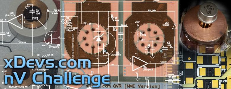
What is this Nanovolt Challenge?

Welcome to this friendly competition dedicated to building some nanovolt-grade hardware and analog designs! This public challenge dedicated for making your own open-source DC Voltage measurement device. Main audience is the electronic design engineers and metrology scientists, who have practical interests in performing very low level DC Voltage signal measurements (microvolt level and below).

Main goal of this contest is to show practical benefits of proposed nanovolt-capable design, not just theoretical possibility of such. There are many new ideas for low-level DC voltage measurements available with modern electronics and advance in digital and analog circuit designs, but very few are actually publicly discussed or demonstrated. This contest main goal is to promote such ideas and show openly what can be achieved in practical accomplished device.  :-/O

Challenge terms and rules

For international metrology community benefits it was decided that each project must comply with next conditions:

* Each submission entry must be based on actual physical design prototype and include design, measurement results and proof of operation.
* Submissions must be completed in 256 days term between September 2, 2021 23:59 EST and May 16, 2022 23:59 EST.
* All design information, including schematics, PCB files (not only Gerbers), libraries, simulation files and source code/firmware files must be publicly available under free to reuse license.
* Wiki or work log write-up about the project (at least 2000 words) with permission to publish it on xDevs.com site.
* There is no budget or component selection limit, as far as previous conditions about public design information is met.
* All designs must come with some sort of verification and performance results data. Noise, gain accuracy, thermal stability (+18 to +28 °C) and linearity parameters data is expected.
* Must not violate any commercial IP or 3rd-party license(s) (e.g. reverse-engineered commercial nano-voltmeter is not OK).
* All submissions must be written in English language.

Bonus point – if you were already working on nanovolt-related project before September 2, 2021, you can reuse any existing hardware, software or firmware and knowledge acquired, given that it should be published within submission entry and released for public as result.

Criteria for project relevance for acceptance

Proposed design must include hardware and software/firmware related to functionality of the unit. Additional calibration and used testing fixtures information is not required but very welcome. To focus design around somewhat common goal each of the nanovolt device entry should be able to perform next functionality to be accepted:

* Have local onboard power regulation. Single common DC (+9 to +24 VDC) or 110/220VAC mains input jack is expected.
* Provide DC Voltage measurement ranges ±100 µV or below and include ±1V and ±10VDC range.
* Have at least two user-accessible input channels for signal to be measured.
* Have low-thermal connection interface to minimize thermal EMF parasitic errors.
* Provide at least 5½-digit resolution for each reading.
* Ability to digitize input DC signal with resolution at least 10 nV and noise better than 30 nV peak to peak over at least 0.1-10 Hz bandwidth.
* Have autozero functionality to correct for static offsets.
* Have galvanic isolated analog front end, with isolation resistance to earth/chassis better than 10 GΩ.
* Device should have ADC (any type) integrated.
* Have good long-term stability and use ovenized DC voltage reference (LM399, LTZ1000 or LTFLU with oven).
* Provide RJ45 Ethernet and/or IEEE-488 GPIB interface for communications with external world / external equipment.
* 40W total input power budget (friendly to battery operation for sensitive experiments)
* Device should be fully operational as standalone device (e.g. no debuggers or external equipment attached to make it work).

Everything else is up to designers, no other limitations or restrictions. References with voodoo-slots, multi-layer PCBs, fancy OLED displays, Raspberry Pi controllers, gold-plated Titanium enclosures – all is welcome.

Compensation for winning project

Since reaching goals of the project are not easy nor simple additional motivation is provided for the best design award.

* Special version of xDevs.com QVR-A module with four of brand new Analog Devices ADR1000 ultra-low noise references.
* Calibration of QVR-A module on Josephson Junction Voltage Quantum Standard (once) with uncertainty below 0.1 ppm.


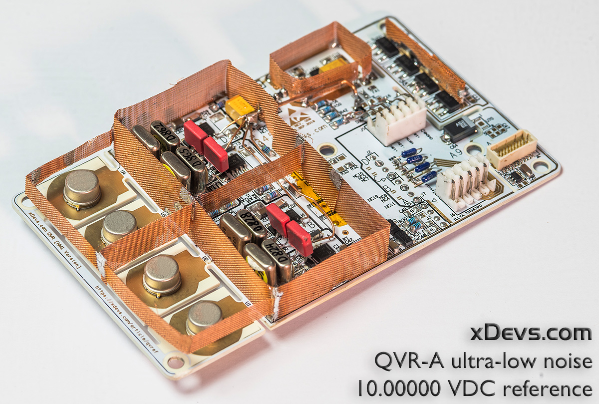
Reference will be packaged in custom rugged aluminum enclosure with low-thermal connectors and protected in hard-case shipping container.

Shipping cost of the QVR-A and JVS calibration will be covered by xDevs.com. Projects will be judged and carefully reviewed after challenge reach the deadline cutout. Final results and ranking will be provided on this page no later than June 16, 2022 23:59 EST. Reference and calibration will be shipped to winner no later than July 31, 2022.

Additional items and prizes might be added in future.

Full details about this challenge contest provided here. Instructions for project submissions are there as well.

Discussion and feedback also can be done in this thread.
« Last Edit: May 17, 2022, 04:14:07 am by TiN »
YouTube | Metrology IRC Chat room | Let's share T&M documentation? Upload! No upload limits for firmwares, photos, files.
 
The following users thanked this post: croma641, bck, jaromir, chuckb, ramon, Irv1n, macaba, I wanted a rude username, Trader

Offline MegaVolt

  • Frequent Contributor
  • **
  • Posts: 917
  • Country: by
Re: Nanovolt design challenge - build and show your own nV-meter in 256 days
« Reply #1 on: September 03, 2021, 10:00:25 am »
Make a Keithley 181 analog in 256 days.

This is a serious challenge...
 
The following users thanked this post: niner_007

Online Kleinstein

  • Super Contributor
  • ***
  • Posts: 14174
  • Country: de
Re: Nanovolt design challenge - build and show your own nV-meter in 256 days
« Reply #2 on: September 03, 2021, 12:37:09 pm »
The Keithley 181 would fail the criteria. Not sure it could measure at a speed to cover the 0.1 to 10 Hz range. This kind of needs at least some 20 readings per second, to really cover it more like 30 or 50 readings per second. Because of mains hum one would kind of need integration over full mains periods. So this would mean using 1 PLC, maybe 2 PLC with no time lost to AZ.
The point noise is a difficult one if it is meant as 30 nV_pp for 0.1 to 10 Hz BW, and not as allowing to measure 0.1 to 10 Hz BW and get the 30 nV_pp noise level at a lower speed.

With "only" the 5.5 digit range, I see no real need for a oven stabilized reference though. It is still easy if the LM399 is available.
 

Offline Psi

  • Super Contributor
  • ***
  • Posts: 9930
  • Country: nz
Re: Nanovolt design challenge - build and show your own nV-meter in 256 days
« Reply #3 on: September 03, 2021, 12:51:46 pm »
* All design information, including schematics, PCB files (not only Gerbers), libraries, simulation files and source code/firmware files must be publicly available under free to reuse license.

Do you mean a open source hardware license that allows free commercial use?

Are the participants going to see a company making and selling their exact design a year later  :-//

I'm not criticizing this, it's just important people know from the start.
It's pretty disheartening when you spend a year of your free time making something awesome for the community
and the next year your product is being sold in the 1000's with a high price tag by some company.

To be clear, this is a cool competition/design challenge and I'm 100% for it, it just need to be transparent on this issue.
« Last Edit: September 04, 2021, 02:06:37 am by Psi »
Greek letter 'Psi' (not Pounds per Square Inch)
 
The following users thanked this post: The Soulman

Offline ramon

  • Regular Contributor
  • *
  • Posts: 143
  • Country: tw
Re: Nanovolt design challenge - build and show your own nV-meter in 256 days
« Reply #4 on: September 03, 2021, 03:50:35 pm »
Thank you Tin for this challenge!

Wouldn't be great if someone provides for free something that is a hit (both technically and economically)?

Wonder if this open contest could translate into colleagues trying to contribute ideas to make something great that could not be possible if each one individually try to beat each other.

Unfortunately, I am not able to contribute any special skill into this task. So I will be just happy to watch how this develops ...

The terms and rules states that ALL must be publicly available, with granted permission to xDevs to publish it. This means to me that it is completely open. Anyone could make the device too, not just one company.

Success would mean that the next year the evil auction site will have tens of sellers selling the PCBs or assembled boards to make our own nanovoltmeter for less than the price of AoE book.

It's not the winning, it's the taking part. So they say!
 
The following users thanked this post: bck

Offline ramon

  • Regular Contributor
  • *
  • Posts: 143
  • Country: tw
Re: Nanovolt design challenge - build and show your own nV-meter in 256 days
« Reply #5 on: September 03, 2021, 04:05:40 pm »
Hey, I am reading the rules again and I think that It's super easy.

5½-digit, 100uv (10nV resolution):

Code: [Select]
+100.00
+ 99.99
+  0.00
- 99.99
-100.00

I have a few ICL7135 here, I think I can have some hack prepared next week.
 

Offline The Soulman

  • Frequent Contributor
  • **
  • Posts: 949
  • Country: nl
  • The sky is the limit!
Re: Nanovolt design challenge - build and show your own nV-meter in 256 days
« Reply #6 on: September 03, 2021, 04:37:01 pm »
* Have local onboard power regulation. Single common DC (+9 to +24 VDC) or 110/220VAC mains input jack is expected.
* Provide DC Voltage measurement ranges ±100 µV or below and include ±1V and ±10VDC range.
* Have at least two user-accessible input channels for signal to be measured.
* Have low-thermal connection interface to minimize thermal EMF parasitic errors.
* Provide at least 5½-digit resolution for each reading.
* Ability to digitize input DC signal with resolution at least 10 nV and noise better than 30 nV peak to peak over at least 0.1-10 Hz bandwidth.
* Have autozero functionality to correct for static offsets.
* Have galvanic isolated analog front end, with isolation resistance to earth/chassis better than 10 GΩ.
* Device should have ADC (any type) integrated.
* Have good long-term stability and use ovenized DC voltage reference (LM399, LTZ1000 or LTFLU with oven).
* Provide RJ45 Ethernet and/or IEEE-488 GPIB interface for communications with external world / external equipment.
* 40W total input power budget (friendly to battery operation for sensitive experiments)
* Device should be fully operational as standalone device (e.g. no debuggers or external equipment attached to make it work).

Why 1 and 10Vdc? must they use the same front-end/connections?
Why Lan or GPIB? no opto isolated serial connection?
Why ovenized v-ref? There are plenty non-ovenized low tempco zeners (good enough for 6 digits) available?
Minimum two in-depended channels with own adc, multiplexed or manual switchable?
Minimum input impedance requirements??

Looks like fun, but a lot of work with a few unnecessary complications.
 
The following users thanked this post: nuclearcat

Online dietert1

  • Super Contributor
  • ***
  • Posts: 2061
  • Country: br
    • CADT Homepage
Re: Nanovolt design challenge - build and show your own nV-meter in 256 days
« Reply #7 on: September 03, 2021, 04:57:20 pm »
...
I have a few ICL7135 here, I think I can have some hack prepared next week.
I think your table and that chip is considered 4 1/2.
Better way to go is an AD7177 or a TI ADS1263. Those have on-chip temperature sensors, so they can be made nV stable even without zeroing by a relay. I think a fairly easy challenge, build something like the HPM7177. There is one for sale in Germany right now and the design is open. Just add a variable gain front-end.

Regards, Dieter
 
The following users thanked this post: ramon

Offline guenthert

  • Frequent Contributor
  • **
  • Posts: 712
  • Country: de
Re: Nanovolt design challenge - build and show your own nV-meter in 256 days
« Reply #8 on: September 03, 2021, 05:17:39 pm »

Why 1 and 10Vdc? must they use the same front-end/connections?
Why Lan or GPIB? no opto isolated serial connection?
Why ovenized v-ref? There are plenty non-ovenized low tempco zeners (good enough for 6 digits) available?
Minimum two in-depended channels with own adc, multiplexed or manual switchable?
Minimum input impedance requirements??

Looks like fun, but a lot of work with a few unnecessary complications.

     Not that I'll be able to compete, but I was wondering the same.  It's easy enough to slap a RPi/Beagle Bone at the end for Ethernet or a AR488 in device mode for GPIB (for new devices? really?), once there is a serial connection, but why make it part of this challenge?

     And yes, instead of specifying an ovenized reference, I'd rather see some 120s / 24h drift specifications.

     Not sure why asking for a 1V and 10V range on a nanovoltmeter (the Keithley 181 has those and they are imho utterly useless as they i) use a different connector there and ii) performance is only mediocre).  I'd rather see a minimum safe input voltage (difference on input as well as common mode) specification.
« Last Edit: September 03, 2021, 05:30:10 pm by guenthert »
 

Online Kleinstein

  • Super Contributor
  • ***
  • Posts: 14174
  • Country: de
Re: Nanovolt design challenge - build and show your own nV-meter in 256 days
« Reply #9 on: September 03, 2021, 07:23:09 pm »
A 1 and 10 V range using the same reference and ADC  are nice sometimes, especially if there is enough resolution.
Requiring a 100 µV range is odd, as this would mean 1 nV resolution (if still 5 digits) - depending on the ADC resolution one may not even need a 1 mV range to get 10 nV resolution. Ok one could allways "cheat" in SW and arificially limit the range. I would guess a 20 V range instead of 10 V should be OK too.

The 1 and 10 V range may be good to test the reference drift. It would add a bit to the challenge if the 10 V need to work from the same terminals.

I would consider the front end the real challenge, the rest is more like easy.
 

Offline maxwell3e10

  • Frequent Contributor
  • **
  • Posts: 869
  • Country: us
Re: Nanovolt design challenge - build and show your own nV-meter in 256 days
« Reply #10 on: September 03, 2021, 07:52:02 pm »
So it's a bit better noise performance than HP 34420, which can do about 70 nVpp at 1NPLC and  30nVpp at 10NPLC.

30 nVpp in 0.1Hz to 10 Hz one can get with a single LT6018 op-amp (if datasheet is to be believed).

One needs to specify a source resistance or current noise level. Also long term gain and offset stability.
 

Offline 1audio

  • Frequent Contributor
  • **
  • Posts: 304
  • Country: us
Re: Nanovolt design challenge - build and show your own nV-meter in 256 days
« Reply #11 on: September 04, 2021, 04:21:24 am »
I got one of these https://quantasylum.com/collections/frontpage/products/qa351-uv-dc-voltmeter some time ago. Its actually pretty close to what is specified.  It does have really good (gigaOhm) isolation from the USB interface. The weakness are BNC input (I added a double banana jack) and the need for an input conditioner/gain to get deeper into the nanovolts. I have tried it between two precision references and its been quite stable. Its not a direct replacement as is for a nanovoltmeter but it suggests a pretty direct path.

One aspect I would suggest for this competition is using a USB interface. Easier possibly and you can get power from the interface and move the analysis off to a PC.
 

Offline TiNTopic starter

  • Super Contributor
  • ***
  • Posts: 4543
  • Country: ua
    • xDevs.com
Re: Nanovolt design challenge - build and show your own nV-meter in 256 days
« Reply #12 on: September 04, 2021, 05:12:07 pm »
Let's address questions.

Quote
Do you mean a open source hardware license that allows free commercial use?

Project should be fully open to benefit everyone. From my end I can only tell that there is no commercial or business interest from me in making or selling anything resulted from this challenge. But others, including author of design is welcome to start an enterprise and sell stuff. It is however niche market and would need serious invenstment to turn into business, so not something you can easily sell "in 1000's next year". Goal is to share the knowledge and educate new generation engineers about difficulty of low level voltage measurements. I'm going to design my own version of device as well (not competing in challenge  ;D).

Quote
I have a few ICL7135 here, I think I can have some hack prepared next week.

+100.00 uV to -100.00 uV was 4.5-digit indeed. I expect ADC side to be very easy/easy, comared to sensitive nV-frontend, where the main challenge is. The requirement to have ADC integrated in project is to rule out designs with just nV-preamplifier box connected to commercial DMM and calling it a day.

Quote
Why 1 and 10Vdc? must they use the same front-end/connections?
So you could quicky check if your DUT performing or what signal is there, before you switch to low voltage ranges (and overload them). Should use same input port (challenge about switching nV-type signals and 10V FS? ;) )

Quote
I'd rather see a minimum safe input voltage (difference on input as well as common mode) specification.
Well, consider 10V as minimum safe input voltage, meaning that nV frontend should not blow up when 10V applied to it (it does not have to be functional, obviously). You never connected 10V DC Voltage reference for opposite measurement in wrong polarity before, having 20V across nV-input, instead of few uV/mV?  :-BROKE
No need to have CAT rating or safety certification for design, it's for laboratory bench use in baby care gloves anyway :)

Quote
Why Lan or GPIB? no opto isolated serial connection?
No serial or USB or SPI/I2C so you could easily integrate meter into bigger experiments with commercial gear.

Quote
It's easy enough to slap a RPi/Beagle Bone at the end for Ethernet or a AR488 in device mode for GPIB (for new devices? really?), once there is a serial connection, but why make it part of this challenge?
Ease of integration was the reason for LAN/GPIB. LAN(VXI) and GPIB are existing infrastructure and allow paralleling many devices without effort. Serial/optical/USB not so much as there is no single standard way and hardware for multi-device with those interfaces. They are fine for one, maybe two devices, but what if you want 8?

Quote
Why ovenized v-ref? There are plenty non-ovenized low tempco zeners (good enough for 6 digits) available?
It's not about tempco, but about long-term stability, so device should not need frequent recalibration.

Quote
And yes, instead of specifying an ovenized reference, I'd rather see some 120s / 24h drift specifications.
No rules or hard specifications here, that would be points for judging from actual designs. Using ovenized reference by default will already make it very good and limited by nV-frontend stability. ;)

Quote
Minimum two in-depended channels with own adc, multiplexed or manual switchable?
Input channels can be switched at the front-end (think as integrated nV-multiplexer? Can be more than 2 channels too).

Quote
Minimum input impedance requirements??

Quote
One needs to specify a source resistance or current noise level. Also long term gain and offset stability.
These are up to designer. Idea is to have and demo performance of different designs with possible different use cases, not some fully specified and polished commercial-grade instrument being built in 256 days.  :-DMM

Quote
I think a fairly easy challenge, build something like the HPM7177.
HPM7177 was motivational for this idea, yes. But with more focus on low level voltage signals, rather than ultimate stability.


« Last Edit: September 04, 2021, 05:25:03 pm by TiN »
YouTube | Metrology IRC Chat room | Let's share T&M documentation? Upload! No upload limits for firmwares, photos, files.
 
The following users thanked this post: bck

Offline armandine2

  • Frequent Contributor
  • **
  • Posts: 596
  • Country: gb
Re: Nanovolt design challenge - build and show your own nV-meter in 256 days
« Reply #13 on: September 04, 2021, 08:53:52 pm »
Let's address questions.
HPM7177 was motivational for this idea, yes.

when I google "hpm7177 open source" something comes up - whether in 256 days from now I'll know much more is doubtful? But from to doubt to to know is the usual way.
Funny, the things you have the hardest time parting with are the things you need the least - Bob Dylan
 

Offline MegaVolt

  • Frequent Contributor
  • **
  • Posts: 917
  • Country: by
Re: Nanovolt design challenge - build and show your own nV-meter in 256 days
« Reply #14 on: September 04, 2021, 09:02:47 pm »
Goal is to share the knowledge and educate new generation engineers about difficulty of low level voltage measurements.
...
The requirement to have ADC integrated in project is to rule out designs with just nV-preamplifier box connected to commercial DMM and calling it a day.
A good amplifier connected to a typical multimeter, in my opinion, will allow to better show the peculiarities of nanovolts and will not have to spend effort on the software interface and ADC.
 
The following users thanked this post: egonotto

Offline TiNTopic starter

  • Super Contributor
  • ***
  • Posts: 4543
  • Country: ua
    • xDevs.com
Re: Nanovolt design challenge - build and show your own nV-meter in 256 days
« Reply #15 on: September 04, 2021, 10:36:02 pm »
It's about system design as well. It's easier to build nV-amplifier, enclose it in magical thermal vacuum chamber and measure a copper short circuit with sub-nV noise.
Completely different story to integrate same amplifier in same box with digital and power supply and then battle for thermal inbalances, noise pickup, magnetic interferences and switching problems, etc.  :-/O
YouTube | Metrology IRC Chat room | Let's share T&M documentation? Upload! No upload limits for firmwares, photos, files.
 
The following users thanked this post: egonotto

Offline ramon

  • Regular Contributor
  • *
  • Posts: 143
  • Country: tw
Re: Nanovolt design challenge - build and show your own nV-meter in 256 days
« Reply #16 on: September 05, 2021, 12:33:40 am »
Goal is to share the knowledge and educate new generation engineers about difficulty of low level voltage measurements. I'm going to design my own version of device as well (not competing in challenge  ;D).

Will that project be open?

Wouldn't be easier if you just post a thread with your requirements and goals and let everyone participate to provide feedback and at the same time being able to reproduce the design and test it with their own gear?

You can divide the project into sections (like connectors area, input stage, ADC, computer interface, ...). And let everyone participate and build their own version. As everyone has its own bias regarding design requirements so this will allow everyone to 'fork' the design into whatever they prefer.  There are many different areas of design that require different skills, so everyone can be mentor or apprentice.
 

Offline TiNTopic starter

  • Super Contributor
  • ***
  • Posts: 4543
  • Country: ua
    • xDevs.com
Re: Nanovolt design challenge - build and show your own nV-meter in 256 days
« Reply #17 on: September 05, 2021, 01:05:03 am »
I think contest challenge is more fun with some additional motivation and much less restrictions for requirements/particular design goals.
I'll also be using EM A10 commercial amplifier, so not much of actual nV-design will be done for my device.
« Last Edit: September 05, 2021, 01:14:54 am by TiN »
YouTube | Metrology IRC Chat room | Let's share T&M documentation? Upload! No upload limits for firmwares, photos, files.
 

Offline ramon

  • Regular Contributor
  • *
  • Posts: 143
  • Country: tw
Re: Nanovolt design challenge - build and show your own nV-meter in 256 days
« Reply #18 on: September 05, 2021, 01:14:53 am »
Let's address questions.
Quote
Why Lan or GPIB? no opto isolated serial connection?
No serial or USB or SPI/I2C so you could easily integrate meter into bigger experiments with commercial gear.
...
Ease of integration was the reason for LAN/GPIB. LAN(VXI) and GPIB are existing infrastructure and allow paralleling many devices without effort. Serial/optical/USB not so much as there is no single standard way and hardware for multi-device with those interfaces. They are fine for one, maybe two devices, but what if you want 8?

Your have very strong prejudice against RS232 and all of your statements are just plainly wrong.

There are plenty of multiple RS232 port interfaces for just the price of a single passive GPIB cable.

Being able to control several devices in parallel is not a protocol or transport issue, it is a control/system issue.

It can be done. RS232 has been in the telecommunication industry for many decades and you can parallel AND synchronize with as many systems as you want. Not to mention that it is simple, easy to implement, cheap, reliable, and has complete documentation available ... to name a few.

But I don't want to start any war. It is completely ok for me. To meet your requirements I plan to use a nice and cheap RS232-to-LAN (RJ45) adapter.  ;)
 
The following users thanked this post: Andreas

Offline Psi

  • Super Contributor
  • ***
  • Posts: 9930
  • Country: nz
Re: Nanovolt design challenge - build and show your own nV-meter in 256 days
« Reply #19 on: September 05, 2021, 03:49:09 am »
Quote
Do you mean a open source hardware license that allows free commercial use?
Project should be fully open to benefit everyone. From my end I can only tell that there is no commercial or business interest from me in making or selling anything resulted from this challenge.
:-+
Greek letter 'Psi' (not Pounds per Square Inch)
 

Online dietert1

  • Super Contributor
  • ***
  • Posts: 2061
  • Country: br
    • CADT Homepage
Re: Nanovolt design challenge - build and show your own nV-meter in 256 days
« Reply #20 on: September 05, 2021, 06:13:56 am »
When TiN writes integration he means automation and wants to make it appear more "professional". But there is no mention of error handling, selftest or ACAL capabilities, nor any incentive for teamwork. Nothing but tinkering.
We'll see whether an open discussion like the one branadic initiated or TiNs challenge will produce something. From branadics thread i learned that the ADS126x is better than the ADS 1256 i recommended before: https://www.eevblog.com/forum/metrology/scannermultiplexers-for-voltage-references/msg3474342/#msg3474342. And from the HPM7177 documents and M. Reps' youtube video i learned we should have the ADC, its reference and its front end in a TEC oven.

Regards, Dieter
 
The following users thanked this post: ramon

Offline tszaboo

  • Super Contributor
  • ***
  • Posts: 7369
  • Country: nl
  • Current job: ATEX product design
Re: Nanovolt design challenge - build and show your own nV-meter in 256 days
« Reply #21 on: September 05, 2021, 08:40:39 am »
To be honest, while at first it looked interesting, the more I read into the post, the more I decided that I couldn't be bothered to make this. Some of the requirements feel just a bit over the top, which would make this from an interesting design challenge to a nightmare.
Ethernet: nope, that means i probably have to spend more time doing linux kernel panic hard faults checking than designing the AFE. Also it pretty much restricts you to work with a single board computer. If you want to automate something, I give you a serial interface, or serial over USB, BOYD and have fun with that.
GPIB: Even worse. Restricts you for boards with plenty of GPIO and it is really high speed. And once again, I want to write as little code as possible.
Ovenized reference: Why? I can select a reference from the top of my head, that would provide this ~4.5 digit accuracy and it would do that for a very long time. And it would output 5V or something that the ADC uses, and the MF ships me one for free if I ask nicely. Instead, I'm supposed to spend something like 100EUR or more getting the REF and Vishay resistors, and not just that, but spend considerable amount of time verifying the characteristics of it. I don't even have the test setup at home to make such measurements. And I'm half sure that the ref wouldn't even be the limiting component in this AFE.
 

Online 2N3055

  • Super Contributor
  • ***
  • Posts: 6599
  • Country: hr
Re: Nanovolt design challenge - build and show your own nV-meter in 256 days
« Reply #22 on: September 05, 2021, 10:01:44 am »
I think contest challenge is more fun with some additional motivation and much less restrictions for requirements/particular design goals.
I'll also be using EM A10 commercial amplifier, so not much of actual nV-design will be done for my device.

I hugely support your initiative to develop an open source instrument for nV measurements, making this kind of measurements more accessible to more people.
But, despite huge respect I have for you and your immense Voltnuting acumen, i must disagree with you on many points.

What you wrote here means that you, for instance, won't be doing ANYTHING technically related to challenge of measuring nano Volts.
Nanovolt measuring challenge is all about device/DUT interconnect, front end , guarding and physical package of all that.

Even if you add A/D converter (that does have some benefits to be included in a device), then only protocol for data out should be exactly RS232 UART. That is dead simple to implement and is well standardized and common on T&M devices...Simple to galvanically isolate too...
And very simple to debug while development.
Ethernet with TCP/IP requires a full computer with protocol stack. That can be added later as an optional thing. You could use RaspberyPi for that, or anything really.

Nanovolt meter should be simple headless design, a box that receives nanovolt on one side and spews RS232 messages on the other. That makes digital side an A/D converter and  a MCU, even an Atmel Mega or equivalent device will do. Simple. Maybe few housekeeping messages. Those can even be SCPI compatible, because it can be easily implemented for those few simple commends.  If you insist on Ethernet, there things like X-port that convert serial UART to Ethernet. Very simple.

And then you can have front panel that has UI that speaks with measurement module. All instruments have that design.
If you take MCU that has 2 UARTs you can speak with front panel and outside world at the same time.

Making it modular something like that also means that different people (that have different skillsets) develop best front end and there can be simple 7-segment display module and also a graphic screen display module if someone wants that...

As for 10 V ranges, since this is not to be high grade meteorological instrument with 8.5 digit accuracy, why would you spend months adding something like that and potentially compromising design, when for cursory check you can use a separate 50 € handheld device?  That everybody already have.

Input should be made to survive 25-30 V P-P constant and to survive basic ESD events.

As for ovenized reference,  I don't mind, price difference is not much. But very stable ovenized reference won't have much correlation on stability of instrument. I expect other things to drift much, much more than reference. If anything, maybe opting for low power reference to make temperature gradients in sensitive analog module less?
Or whole analog module made on alu substrate board and ovenized ? In which case heated reference is not so much a problem...

Cheapest way to do nanovolt measurements today is to, exactly like you, buy EM Electronics amplifier and connect it to your bench meter.
If community endeavours to such a big task, frankly, there must be some benefit from it: either sub 200€ price (so benefit is being more affordable) or some advanced features, which can be very good analog performance (very hard to do) or maybe if a modular approach is adopted, fact that you can for instance only use front end module  and use it only as data acquisition module and pull data directly to PC with Python code or Scilab/Octave/Mathlab.  Or use of module integrated as a part of a micro ohm meter, or whatever you think off..

Best,
« Last Edit: September 05, 2021, 10:05:48 am by 2N3055 »
 
The following users thanked this post: The Soulman

Offline ramon

  • Regular Contributor
  • *
  • Posts: 143
  • Country: tw
Re: Nanovolt design challenge - build and show your own nV-meter in 256 days
« Reply #23 on: September 05, 2021, 10:29:28 am »
My solution for the PC interface is cheap ($10-20) and completely hassle free. No programming, no driver needed, no high speed CPU or SBC needed. The simplicity of rs232 with an rj45 connector.  Google: "usr-k5", "usr-k7", "usr-tcp232-s2".

About the ovenized reference, here I agree with Tin about having at least a LM399. It is not too expensive, not so difficult to buy, doesn't require too many expensive extra components, and its long term performance is know. (Too noisy, is maybe the only issue)

But, yes, you are rigth that many 5 digits and half meters have been done with lt1027, lt1021 or many other references. I have seven lt1021bcn8-7 (the version with 7 volts output for maximum long term stability) in a drawer. I was surprised about the stability and low noise when I tested one sample. Don't know if TIN would accept them inside an oven.
 
The following users thanked this post: I wanted a rude username

Offline jaromir

  • Supporter
  • ****
  • Posts: 337
  • Country: sk
Re: Nanovolt design challenge - build and show your own nV-meter in 256 days
« Reply #24 on: September 05, 2021, 03:16:19 pm »
Thank you TiN.
I like this contest very much. Yes, it's got non-trivial requirements, but that is a part of the game. :-+
 
The following users thanked this post: TiN


Share me

Digg  Facebook  SlashDot  Delicious  Technorati  Twitter  Google  Yahoo
Smf