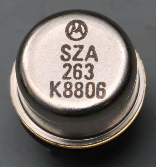
Author Topic: The LTFLU (aka SZA263) reference zener diode circuit  (Read 197644 times)

0 Members and 1 Guest are viewing this topic.

Online iMo

  • Super Contributor
  • ***
  • Posts: 4780
  • Country: pm
  • It's important to try new things..
Re: The LTFLU (aka SZA263) reference zener diode circuit
« Reply #500 on: January 24, 2021, 04:42:34 pm »
@dietert1: I've made a table based on a lecture here


taking into account walls, edges and corners of the Box. There are the edge and corner "coefs" which depend on a ratio of the box sizes to the wall thickness, however.

Added the heat transfer via copper.

Added the xls file.

Maybe a topic for a separate thread..


« Last Edit: January 25, 2021, 09:37:21 am by imo »
 
The following users thanked this post: chuckb, MegaVolt

Offline dietert1

  • Super Contributor
  • ***
  • Posts: 2070
  • Country: br
    • CADT Homepage
Re: The LTFLU (aka SZA263) reference zener diode circuit
« Reply #501 on: May 21, 2021, 08:22:09 pm »
Here i have a log of two LTFLU references that i made last year (schematic and images above). Nominal oven temperatures are 17.4 °C and 27.69 °C. The voltage difference was recorded with a HP 3456A. Each blue dot represents the average of about 17 000 measurements with 100 PLC and Autozero.
There is a one month gap between 5000 and 6000 hours, when i cleaned the air filter of the HP3456A and used it for other measurements. I also removed three days of data after an unnoticed oven shutdown, when the 17.4 °C oven went up to 28 °C for more than 24 hours. Added an exponential decay fit. Since this was a first crude setup i can't tell which process this may be. There are no significant correlations with ambient temperature, nor humidity, nor barometric pressure.
Next time i want to log multiple references, including a 5x LM399 device and a revision of the LTFLU shown above.

Regards, Dieter
 
The following users thanked this post: SilverSolder, BU508A, chuckb

Offline dietert1

  • Super Contributor
  • ***
  • Posts: 2070
  • Country: br
    • CADT Homepage
Re: The LTFLU (aka SZA263) reference zener diode circuit
« Reply #502 on: June 05, 2021, 06:21:44 pm »
These are 10 V references both including a gain stage inside the same oven. In the 17.4 °C reference the gain stage has 10x UPF25 100R resistors, in the other one the divider is made from three Dale RS5 wirewound resistors of 750R and 150R plus 180R that i found in a drawer. Impressed by the stability of those wirewound resistors i ordered several lots of Vishay Dale RS02 750R and 330R resistors that are similar except smaller. Those resistors need selection if you want TC below 5 ppm/K, but then i found several with very low TC in the interesting temperature region around 25 to 30 °C.
I am running the reference ovens at relatively low temperatures as i want battery backup. In fact those LTFLU references have seen power outages and oven shutdowns without "jumping around". The 17.4 °C oven was the first serious attempt and it works well, but that TEC takes 1 W or more, while the other one at 27 °C runs from 50 to 100 mW due to self heating.
Another alternative to make a low TC gain stage is a PWM circuit as i recently showed in the LM399 thread. Something similar can be nice with a LTZ1000 reference.

Regards, Dieter
 

Offline branadic

  • Super Contributor
  • ***
  • Posts: 2390
  • Country: de
  • Sounds like noise
Re: The LTFLU (aka SZA263) reference zener diode circuit
« Reply #503 on: June 05, 2021, 07:23:43 pm »
I guess you mentioned yourself, that your PWM approach might be good for an LM399, but as far as I understood isn't for an LTZ or LTFLU, due to:

"My PWM prototype has an offset of 11 ppm (max of log). The PWM ratio remained unchanged after implementation. In my opinion a more perfect PWM divider would be more accurate, i mean without tuning or "calibrating" it. Accuracy depends on the symmetry of the PWM switches: resistance and/or timing difference. At 10 KHz a 1 nsec timing asymmetry makes 10 ppm. IC muxes have delays of about 50 nsec that can easily contribute an asymmetry of 1 nsec..."

On the other hand the approach using a TOMC1603 resistor network including parallel resistors for trimming the gain as I did on my LFTLU  reference (even a TDP1603 would do) worked quite good, as it is part of the ovenized aluminum board with the LTFLU. This is though a totally different story, when the gain stage including the parallel resistors for trimming are exposed to ambient temperature changes.

An approach not discussed yet is the gain stage used in W/F7000, that can now be discussed thanks to the reverse engineering by chekhov. Is uses resistor networks for a coarse amplification and adds additional voltage for fine trimming provided by parallel DACs, so no clocking being involved.

-branadic-
Computers exist to solve problems that we wouldn't have without them. AI exists to answer questions, we wouldn't ask without it.
 

Online Kleinstein

  • Super Contributor
  • ***
  • Posts: 14192
  • Country: de
Re: The LTFLU (aka SZA263) reference zener diode circuit
« Reply #504 on: June 05, 2021, 08:07:34 pm »
The on resistor matching is mainly a thing with linearity and only to a small part with temperature drift. An offset due to delays and charge injection is likely quite stable. For a gain stage we don't need good linearity or a very low offset. The main point is long term drift. The more problematic point may be EMI. Chances are a lower PWM frequency could help - however there is a slight complication: in the feedback path it is tricky to use more than a 1 st order filter. So residual ripply could become a problem with a much lower frequency, unless one could reduce the ripple in a different way (e.g. the compensation with an opposing signal).

For a stable ration there would also be the option to use a charge pump (e.g. LTC1043) for the coarse part (Faktor 1.5) and than use resistors for the fine part only.

Anyway it gets a bit off topic from the LTFLU ref., though the ref and gain are closer coupled with the LTFLU - at least in the normal circuit.
 

Offline dietert1

  • Super Contributor
  • ***
  • Posts: 2070
  • Country: br
    • CADT Homepage
Re: The LTFLU (aka SZA263) reference zener diode circuit
« Reply #505 on: June 05, 2021, 09:13:32 pm »
My plan outlined in the LM399 thread is to reduce PWM frequency from 10 KHz to 1 KHz (or 1200 Hz  = multiple of 50 and 60 Hz). For this i implemented ripple compensation as shown in the schematic. Then you have a 2nd order filter that behaves better than a third order filter as ripple compensation helps on PWM input and output side. This change gives me a factor 8 or 10, so the 11 ppm becomes about 1 ppm.
Then you want another factor ten of precision. This happens by the implementation of a discrete PWM output stage as we see them in Fluke/Wavetek/Datron calibrators. I already posted a study/proposal for a discrete PWM output stage. By combining everything one should arrive at a PWM with about 0.1 ppm absolute accuracy. If PWM stability will be another factor ten better than absolute accuracy as observed with the current circuit then that PWM gain stage will be good enough for scaling a group of LTZ1000s to 10 V.
Currently i am rebuilding my metering setup so i can check long term stability at a 100 nV level or below. I want to integrate four references: The two LTFLUs with analog gain stage inside oven, the 5x LM399 with improved PWM gain stage and a 10 V double JFET reference without gain stage. And of course there should be at least one unused port for testing other references..

Regards, Dieter
 

Online Kleinstein

  • Super Contributor
  • ***
  • Posts: 14192
  • Country: de
Re: The LTFLU (aka SZA263) reference zener diode circuit
« Reply #506 on: June 06, 2021, 06:20:43 am »
For testing the reference and gain stages it would make sense to not only compare the scaled 10 V level, but also check drift of the raw reference voltage before scaling. The dirft of the 2 parts can be comparable.

For the PWM switches I would not count much on better performance from discrete switches compared to modern CMOS switch chips. The discrete solution may have more EMI issues and more charge injection.
The ripple compensation with the capacitive coupled inverted signal acts like an addional filter stage for the PMW part, but not adding much phase shift to the loop. So the ripple reduction is likely a good idea.
Another possible option would be 3 phase PWM, so 3 stages with 120 deg. phase shift, which would cancel the main ripple at 1/3 and 2/3 PWM setting and still reduced ripple close to those values.
More switches make discrete switches less attractive.
 

Offline dietert1

  • Super Contributor
  • ***
  • Posts: 2070
  • Country: br
    • CADT Homepage
Re: The LTFLU (aka SZA263) reference zener diode circuit
« Reply #507 on: June 06, 2021, 02:45:26 pm »
I did my work and later wrote about a discrete implementation of a precision PWM output stage. My schematic in the LM399 thread shows a circuit i built and tested to some degree. As always there may be other solutions and i will be interested in other substantial proposals.
In my prototype i used a FDC6561AN dual mosfet with Rdson = 0.1 Ohm and about 0.03 Ohm match. If somebody wants to propose an IC switch with lower Rdson and/or better Rdson matching, you are welcome. In a totem-pole circuit with optimized dead time you can forget about charge injection.

Regards, Dieter
 

Online Kleinstein

  • Super Contributor
  • ***
  • Posts: 14192
  • Country: de
Re: The LTFLU (aka SZA263) reference zener diode circuit
« Reply #508 on: June 06, 2021, 04:50:01 pm »
The  FDC6561AN are interesting in that they allow a relatively high gate voltage. Many other modern FETs have the protection start engaging at some 10-15 V already.
 
However I don't think these rather large FETs would be a good choice for precision PWM. The gate capacitance is quite large and this leads to quite some current spikes at the driving side and the supply / gate driver. CMOS switch chips have a much smaller current spike to the input side driver. The charge injection would be a measure for the current pulse to expect. I am afraid that by avoiding the switch resistance effect by all costs, the larger spike towards the driver would cause trouble that is difficult to solve.
It also helps to have the supply separate from the switch connection. So some of the gate driver chips are not a good option, if they have a common supply for the output stage and internal driver.

Instead of the brute force very low resistance way, I would prefer compensation of the switch resistance, like in the Fluke 57xx series. So have a 2nd pair of switches with a slightly higher votlage to  provide essentially all the current. With integrated switches using 2 channels is no that bad.
Anyway for just a 7 to 10 V stage I would not worry so much about a little offset / nonlinearity. One can usually adjust the PWM ratio to get extact 10 V. There is no need to get it from the upfront calculated ratio.

My current favorite for a 7 to 10 V step is 3 phase PMW with 3 x DG419LE  (vishay  - maxim seems higher resistance) going to a common filter with relatively high resistance (e.g. 100 K range each). R_on is at some 15 ohms with matching in the 1 Ohms range. Over some 10 C temperature change this would change by something like 50 mOhms or some 2 ppm change relative to the 100 K filter resistance.
For capacitor leakage and amplifier bias the 3 channels are in parallel so that the overall resistance is not that high.
With relativly low charge injection the spikes effecting the drive should not be that bad. With a PWM ratio close to 2/3 the residual ripple to start with would be small, similar to better than with the coupled opposite phase compensation (which act like a separate filter stage).


Offline dietert1

  • Super Contributor
  • ***
  • Posts: 2070
  • Country: br
    • CADT Homepage
Re: The LTFLU (aka SZA263) reference zener diode circuit
« Reply #509 on: June 06, 2021, 06:02:16 pm »
No, don't agree. My experience tells me that absolute accuracy is THE criterion. If you start fine tuning and adjusting at the 10 ppm level, you will never realize a circuit better than 0.02 ppm as required with a LTZ1000 (let's assume 200 nV). Just read the PWM discussion of branadic and Andreas in the LM399 thread.
The discrete PWM output stage i proposed recently is one way of solving the Mosfet drive problem you were speculating about. Your discussion does not replace a demonstration. Then you will learn to solve problems instead of inventing objections.

Regards, Dieter
 

Offline dietert1

  • Super Contributor
  • ***
  • Posts: 2070
  • Country: br
    • CADT Homepage
Re: The LTFLU (aka SZA263) reference zener diode circuit
« Reply #510 on: June 20, 2021, 08:04:55 pm »
Recently there was a discussion about "reference oven gain".  Today i have a result for our LTFLU ovens (image above).
These ovens have two temperature sensors: One NTC that is kept at constant temperature by the heater. Another temperature sensor is on-chip, derived from the TC of the transistor Ube. The setup also includes a JVR in a similar oven, with a diode as DUT temperature sensor (not on chip but close). The setup also includes two ambient temperature sensors (SHT = humidity and temperature, BMP = pressure and temperature). The first plot shows a log of the two ambient sensors (left y axis) and of the three DUT temperatures (righ y axis = deviation from average). The other diagram shows the correlation. The three line fits give values of about 0.02. That means the three oven gains are about 50. This is the suppression of ambient temperature changes by the oven.
Next step is fine control of the set temperature of each oven as a function of ambient temperature (pre) and DUT temperature (loop).

Regards, Dieter
 
The following users thanked this post: SilverSolder, BU508A, 2N3055

Offline MegaVolt

  • Frequent Contributor
  • **
  • Posts: 917
  • Country: by
Re: The LTFLU (aka SZA263) reference zener diode circuit
« Reply #511 on: September 22, 2021, 12:26:48 pm »
To get a better understanding I have redrawn the schematics of the Fluke 5440 voltage reference.

I also made a list of devices with SZA263 inside.
 
The following users thanked this post: chickenHeadKnob, TiN, Echo88, Dr. Frank, doktor pyta, chuckb, guenthert, ch_scr

Offline TiN

  • Super Contributor
  • ***
  • Posts: 4543
  • Country: ua
    • xDevs.com
Re: The LTFLU (aka SZA263) reference zener diode circuit
« Reply #512 on: September 22, 2021, 01:04:38 pm »
MegaVolt newer devices like DMM7510, 5730/5720B, 732C, 85x8, etc do not use SZA263, but FLU1 chip. It's not the same thing.
Also some older 8508A use Datron LTZ module, newer ones use FLU1.
YouTube | Metrology IRC Chat room | Let's share T&M documentation? Upload! No upload limits for firmwares, photos, files.
 
The following users thanked this post: MegaVolt

Offline MegaVolt

  • Frequent Contributor
  • **
  • Posts: 917
  • Country: by
Re: The LTFLU (aka SZA263) reference zener diode circuit
« Reply #513 on: September 22, 2021, 01:15:58 pm »
Yes. I guess I need to be more specific.
I cheated off you, by the way :)))))))))))) https://xdevs.com/article/ltflu_ref/
 

Offline alm

  • Super Contributor
  • ***
  • Posts: 2881
  • Country: 00
Re: The LTFLU (aka SZA263) reference zener diode circuit
« Reply #514 on: September 22, 2021, 01:33:15 pm »
Don't forget about the Fluke 8800A DMM. Probably the lowest spec device that contained an SZA263. Whether it was binned differently is anyone's guess.
 
The following users thanked this post: MegaVolt

Offline dietert1

  • Super Contributor
  • ***
  • Posts: 2070
  • Country: br
    • CADT Homepage
Re: The LTFLU (aka SZA263) reference zener diode circuit
« Reply #515 on: September 22, 2021, 06:06:53 pm »
That LTFLU report of branadic linked above certainly wins the prize for the most sophisticated way to build a reference worse than a LTZ1000. There is a LTFLU involved, but that may be misleading. Seems like real voltnuts prefer bad setups "for the adventure".

I have seen very good results from various LTFLU references, see above. I did not use "nearby" temperature sensors, but on-chip temperature sensors (similar to LTZ1000, schematic above).
And i used more zener current. In the ADR1000 datasheet they estimate that noise is inversely proportional to the square root of zener current. For an array like the LTFLU i found that each of the four zeners should get at least 2 mA, so 8 mA total. That worked well.
Recently i thought: What could be the performance and the price of an array of 20 000 burried zeners? You know that number is the array size of those superconducting Josephson standards. Power consumption would be about 500 W, i guess less than a Josephson standard. The LTFLU is the only zener array we have. Meanwhile i started making arrays of LM399s, also with promising results.

Regards, Dieter
 

Offline branadic

  • Super Contributor
  • ***
  • Posts: 2390
  • Country: de
  • Sounds like noise
Re: The LTFLU (aka SZA263) reference zener diode circuit
« Reply #516 on: September 22, 2021, 06:56:31 pm »
Another valuable comment by dieter1 with the absence of social skills, brilliant.  :-+
I don't see why you think the reference implementation is "most sophisticated", it's simply a copy of the implementation done in several Fluke gear, but with an additional oven around it, similar to what is realized in Fluke 57xx calibrators and instead of selected ref amp resistors it's using a resistor network. So what is your point?

-branadic-
Computers exist to solve problems that we wouldn't have without them. AI exists to answer questions, we wouldn't ask without it.
 

Offline MegaVolt

  • Frequent Contributor
  • **
  • Posts: 917
  • Country: by
Re: The LTFLU (aka SZA263) reference zener diode circuit
« Reply #517 on: September 23, 2021, 09:50:41 am »
MegaVolt newer devices like DMM7510, 5730/5720B, 732C, 85x8, etc do not use SZA263, but FLU1 chip. It's not the same thing.
Also some older 8508A use Datron LTZ module, newer ones use FLU1.
Corrected.
 

Offline MegaVolt

  • Frequent Contributor
  • **
  • Posts: 917
  • Country: by
Re: The LTFLU (aka SZA263) reference zener diode circuit
« Reply #518 on: May 27, 2022, 10:14:22 am »
I made a model of one stage of the reference source from Fluke 5440. R4 coarse current adjustment. R5 is an exact substring of the maximum of temperature.

R4 differs from the original circuit because a different zener diode is taken.
 

Offline dietert1

  • Super Contributor
  • ***
  • Posts: 2070
  • Country: br
    • CADT Homepage
Re: The LTFLU (aka SZA263) reference zener diode circuit
« Reply #519 on: May 27, 2022, 02:40:22 pm »
Sorry but the voltage divider R4/R1 hardly reaches the zener voltage, so zener current will very small. I can't understand how you got that diagram.

Regards, Dieter
 
The following users thanked this post: MegaVolt

Offline MegaVolt

  • Frequent Contributor
  • **
  • Posts: 917
  • Country: by
Re: The LTFLU (aka SZA263) reference zener diode circuit
« Reply #520 on: May 27, 2022, 03:33:34 pm »
Sorry but the voltage divider R4/R1 hardly reaches the zener voltage, so zener current will very small. I can't understand how you got that diagram.
Hmm.... Indeed the result is not correct.
For other values of R4, it is not possible to obtain a parabotlic curve. Only linearly increasing. Perhaps this zener diode is not suitable.

I need to fix something...
 

Offline Noopy

  • Super Contributor
  • ***
  • Posts: 1732
  • Country: de
    • Richis-Lab
Re: The LTFLU (aka SZA263) reference zener diode circuit
« Reply #521 on: September 21, 2022, 02:18:31 pm »


Finally, a SZA263!  8)
I got it from a really dead FLuke 8842A.


Let´s see if I got everything right:

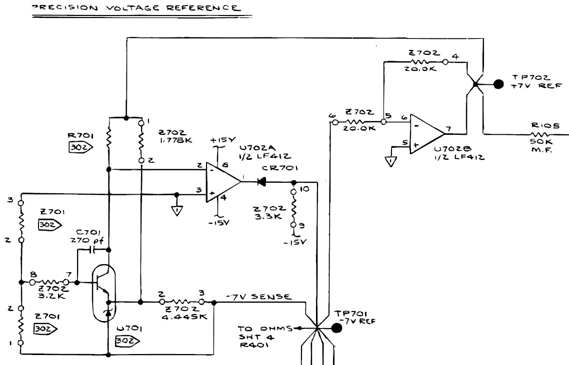
The servicemanual of the Fluke 8842A shows the structure of the SZA263 (U701). The base-emitter path of the transistor provides a negative temperature coefficient. The Z-diode offers a positive temperature coefficient. Suitably designed, there is a current at which the temperature coefficients balance out and the voltage between base and anode exhibits a vanishing temperature drift.

If the temperature drift of a Z-diode is compensated with a pn junction operated in "forward mode" this is just a temperature compensated Z-diode, as for example the 1N829A is (https://www.richis-lab.de/REF22.htm). A ref-amp contains a transistor instead of a simple diode for temperature compensation. The transistor in addition drives the first control loop.

In steady state the opamp U702A ensures that a voltage of -7V is present at the testpoint TP701. In this state voltage divider Z701 sets a base current in SZA263 via base resistor Z702_8-7 that is exactly the current at which the Ref-Amp temperature coefficient becomes minimum. The basic reference voltage is applied between the base and anode of U702. Voltage divider Z701 scales this voltage to the desired output voltage of -7V. If the voltage deviates from -7V, more or less current flows through SZA263, which changes the voltage drop across resistor R701 via the collector of SZA263. The opamp U702A then readjusts the -7V reference voltage accordingly.

I´m not 100% sure with Z702_1-2 and Z702_2-3. Apparently they do some biasing. But they shouldn´t be necessary. Perhaps they compensate the fluctuation of the remaining temperature coefficient a little.

U702B ultimately generates a +7V reference voltage from the -7V reference voltage. Z702_9-10 is the bias resistor of the opamp U702A. Diode CR701 ensures that the voltage at testpoint TP701 does not become positive when the circuit starts up.


Resistor R701 defines the current flowing through the SZA263 and must be set to hit the point of minimum temperature coefficient. The voltage divider Z701 defines the reference voltage. The exact values of the resistors are correspondingly critical. R701 is a precision resistor from Dale. Z701 is a special balanced resistor network.

Accordingly, the Fluke 8842 servicemanual does not individually identify Ref-Amp U701, resistor R701, and resistor network Z701 in the part list. If one of these components is needed, one has to order a "REF AMP SET" which contains all three components and all of them have to be exchanged. The resistors are adapted to just the one SZ263 so that the temperature drift is minimal and the reference voltage is -7V or +7V.


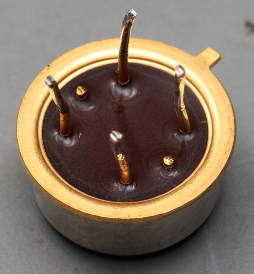
On the bottom of the SZA263 it can be seen that the case would have two more pins in addition to the four that are used. The additional pins have been shortened.


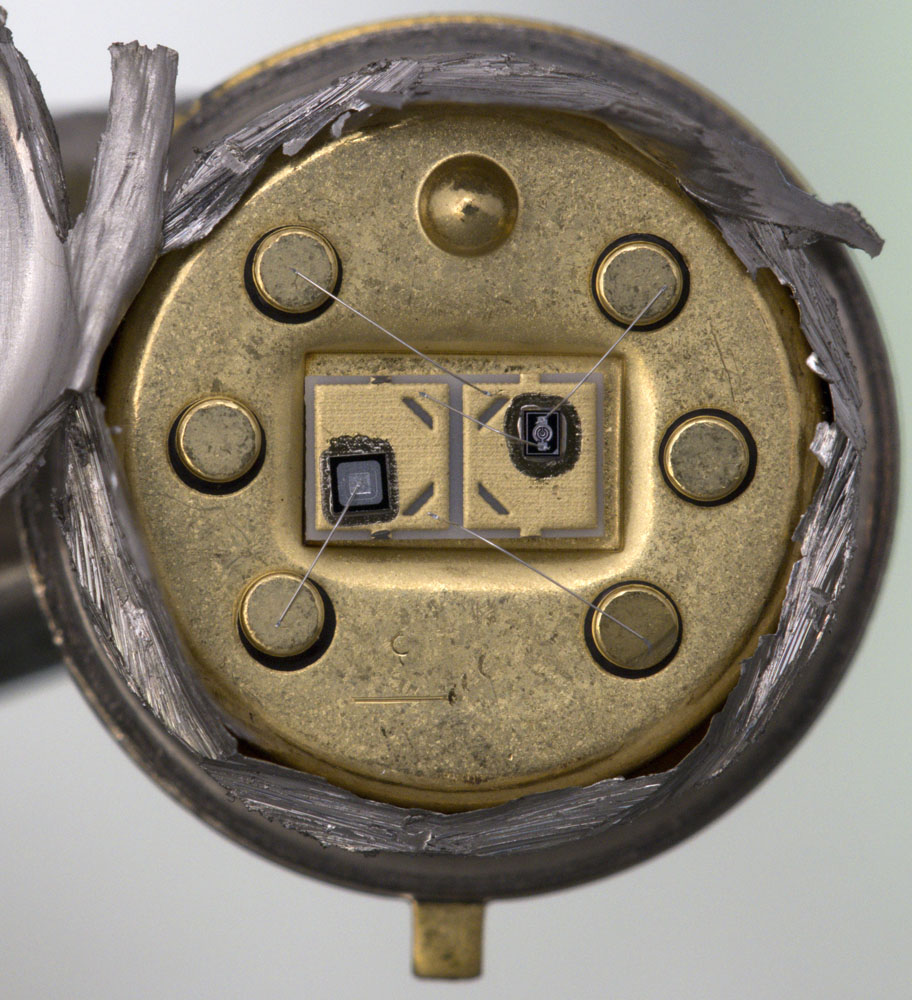
The additional pins are not contacted in the package.


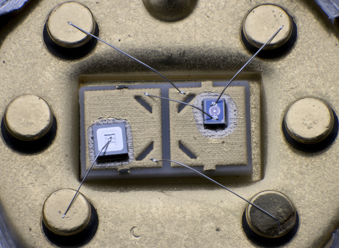
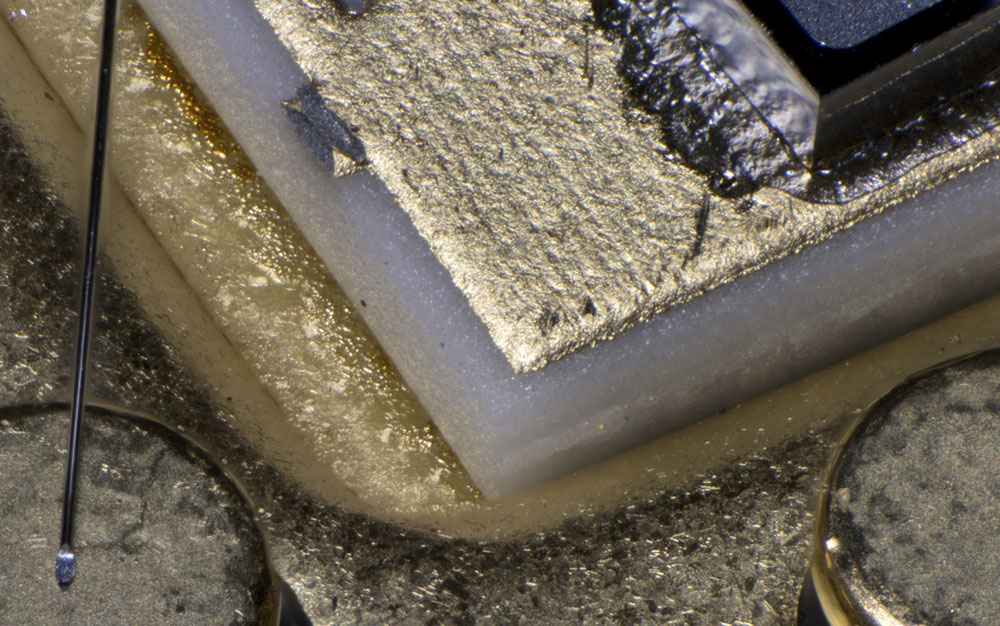
The Z-diode and the transistor are located on a ceramic substrate, which is fixed in a recess of the housing. The package itself is not connected to any of the potentials.


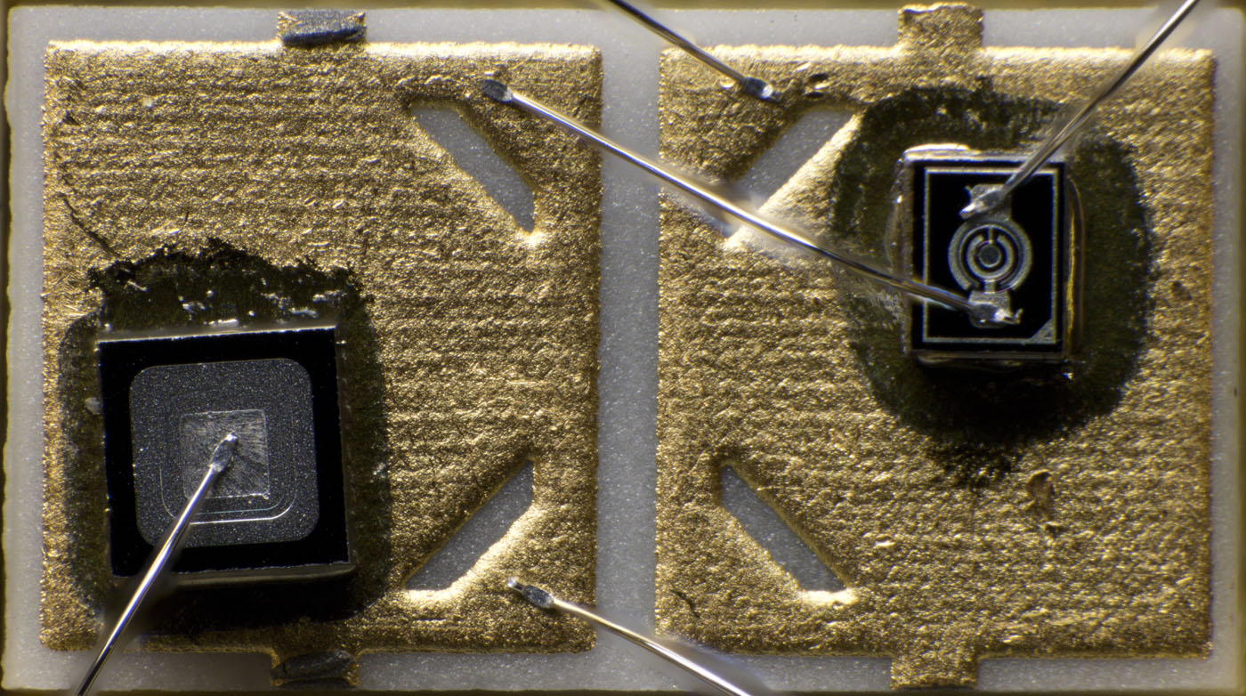
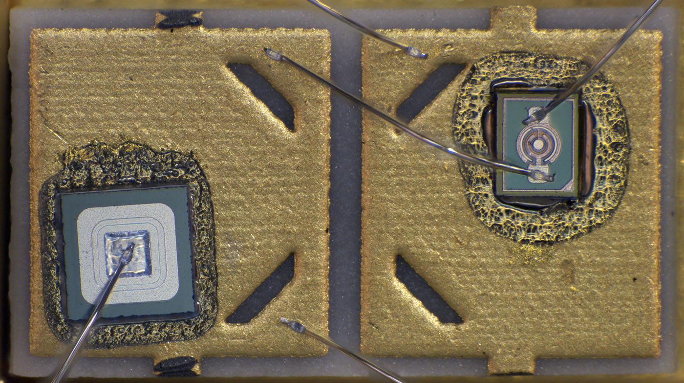
Two metal surfaces are applied to the ceramic substrate. The short lead residues leading to the edges indicate that a larger ceramic element was electroplated with the desired structures during production and then got separated.


The edgelength of the diode is 0,59mm. The uneven surface in the center of the metal layer is reminiscent of the Z-diodes in the reference voltage source VRE305A (https://www.richis-lab.de/REF21.htm#ZD) and in the digital-to-analog converter DAC80 (https://www.richis-lab.de/DAC02.htm#ZD).


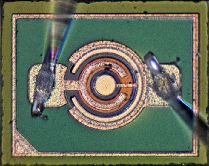
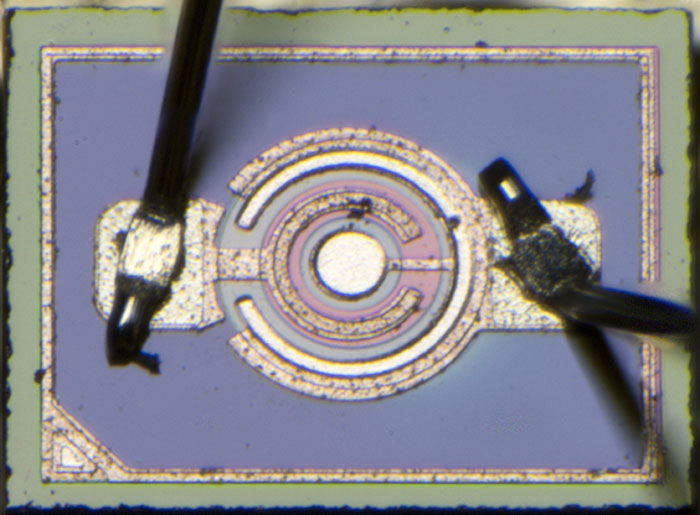
The dimensions of the transistor are 0,48mm x 0,38mm. The ring-shaped emitter is striking. The underlying base area is contacted inside and around the ring. The area of the base-emitter junction is a critical point when matching the temperature coefficient of the transistor to the temperature coefficient of the Z-diode.


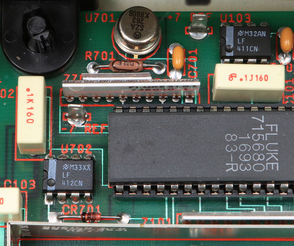
Here you can see the SZA263 in the Fluke 8842A bench multimeter. Below the SZA263 is the precision resistor R701 from Dale (411.62kΩ). Below that, the two resistor networks Z701 and Z702 are placed right next to each other. Most likely, the proximity was deliberately set up to keep the temperatures of the resistors as equal as possible. In the lower left area of the picture the operational amplifier U702 can be found.


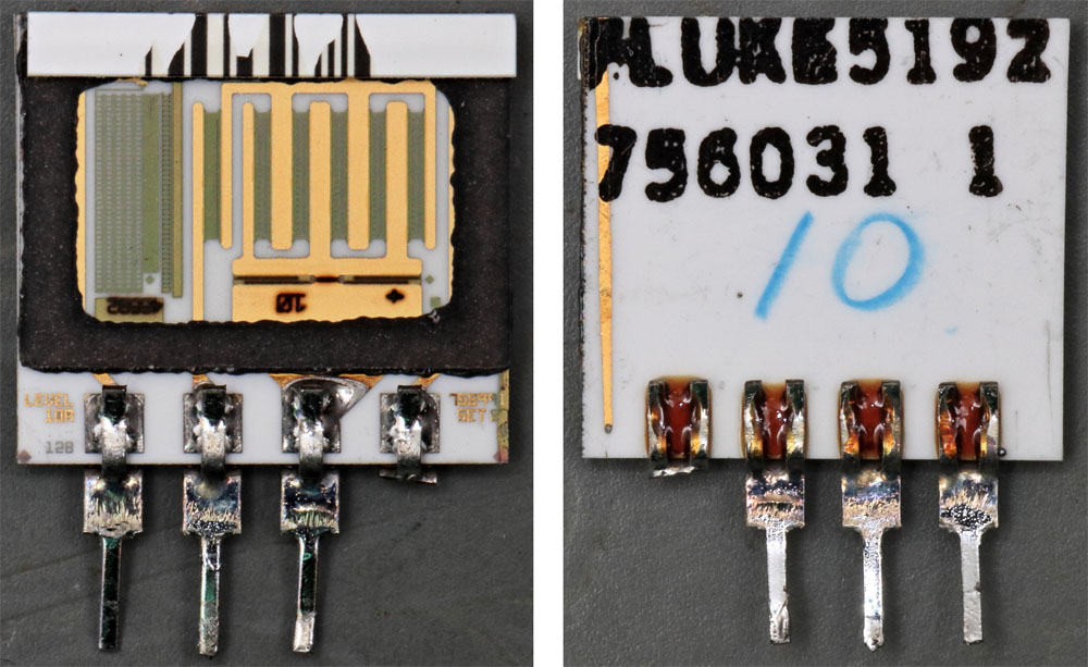
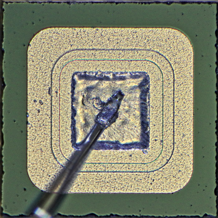
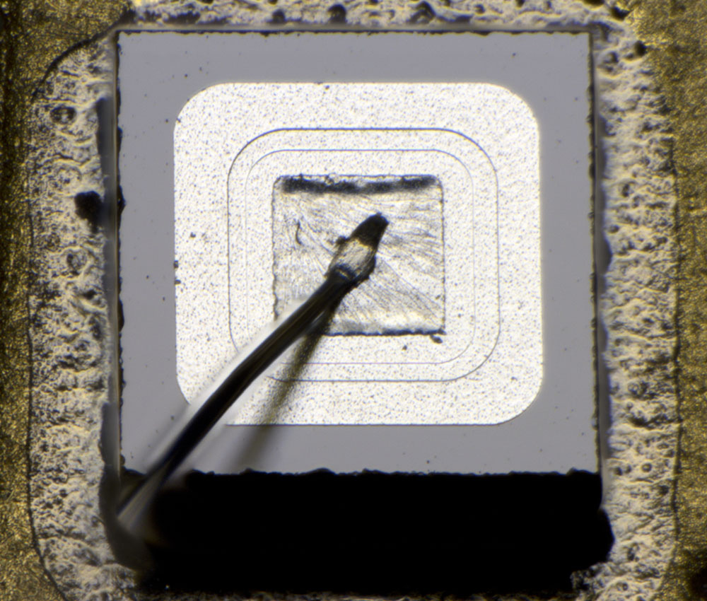
The resistor network Z701 that sets the ideal current through the SZA263 is listed as part number 756031. It is noticeable that the resistor network originally had four connection pins, one of which has been cut off.

The resistors are placed on a ceramic substrate and are protected with a glass cover. The setup allows laser alignment at any time. For high-precision circuits, such a resistor network can be incorporated into an assembly and laser alignment can be performed as a final process on the completed circuit. In this way, it is also possible to compensate for disturbances that occur during a soldering or aging process.


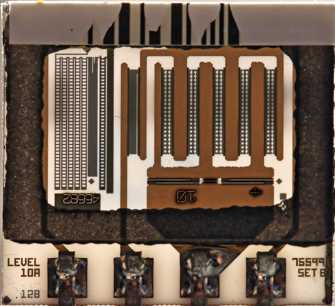
The leads on the ceramic carrier appear to have been gold plated. Each resistor consists of many different geometries, which make it easier to exactly set the desired resistance value.

A closer look reveals that it is not just two resistors. There is a third resistor on pin 2 that acts as an additional base resistor for the SZA263. Pin 4 allows to contact the common node of the three resistors, which makes the adjustment easier. The following resistor values can be determined (referring to the schematic above):
Voltage divider "1-2": 10,582kΩ
Voltage divider "2-3": 202,28Ω
Additional base resistor: 643,67Ω


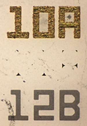
At the bottom left of the ceramic substrate, three masks can be seen. Mask 10A defines the structures of the conductive paths. Mask 12B forms the resistors. The B suggests that this mask was reworked once. Between the masks 10A and 12B you can guess the characters 11A. It seems that this is the mask that defines the transition points between traces and resistors. Apparently, a special treatment of these areas was necessary.


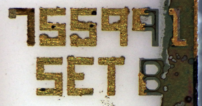
The labeling on the lower right corner of the ceramic carrier shows that the original designation of the resistor network is not 756031 but 755991.


Here we have seen that in the 8842A (with SZA263) Fluke used also a different resistor network. This one actually has just three pins. No additional base resistor can be seen. Apparently, it was advantageous to make the base resistor adjustable in the Ref-Amp package. Maybe it was also possible to use another already existing resistor network.


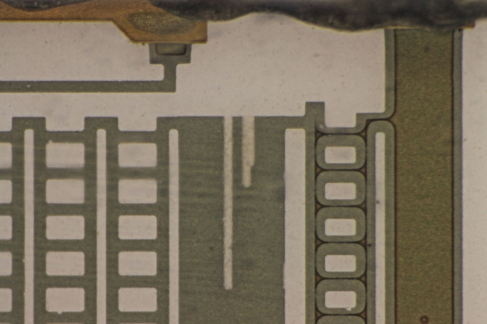
At the upper contact you can see that the second mask is relevant for the contact areas between trace and resistor. In the right area you can see that a large part of the resistor material has been prepared to contact a trace. Probably the resistor network 755991 can represent two very different resistor values here. Once the right area is just contacted at the upper edge, another time an extended trace bridges the right two resistor strips.


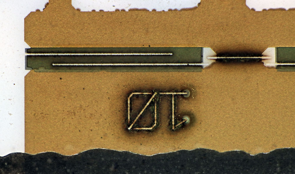
Not only the resistor surfaces, but also the conductor paths were cut with a laser. The labeling most likely serves the traceability of the alignment process.


With the inscription in the left area, one can see that the adjustment was made after the ceramic carrier was sealed. The remains of the inscription process have settled on the glass.


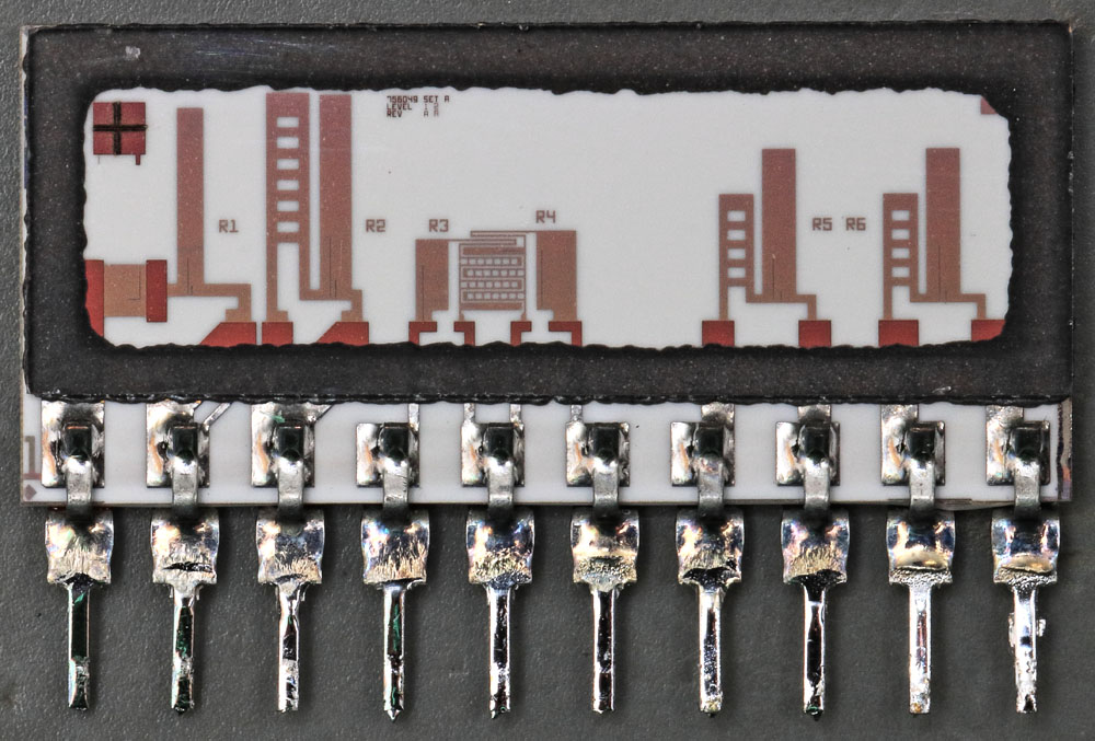
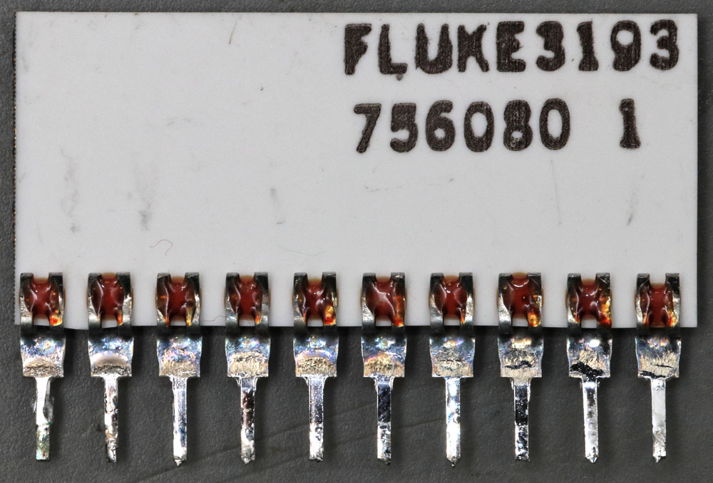
The second resistor network is called 756080. According to the optical appearance, the conductors are made of bare copper. In any case, it is not gold.


The individual resistors can be clearly seen. The resistance values are:
1-2: 1,7783kΩ
2-3: 4,4461kΩ
4-5: 20,005kΩ
5-6: 20,005kΩ
7-8: 3,2007kΩ
9-10: 3,3008kΩ


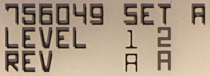
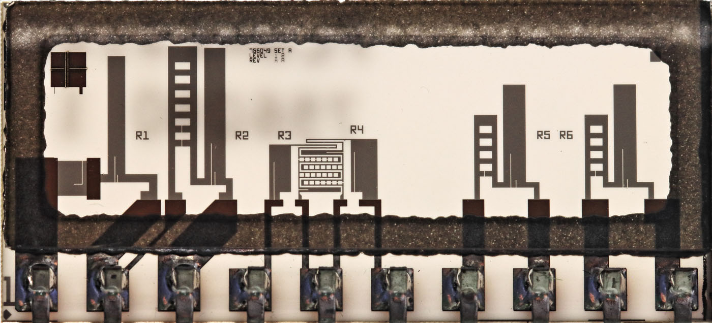
Here, too, a different number can be found on the ceramic carrier: 756049.

A mask for connecting the resistor surfaces with the conductor tracks cannot be seen.


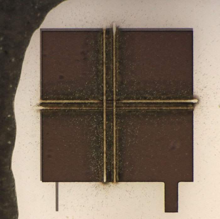
Laser tuning alignment.


https://www.richis-lab.de/REF24.htm

 :-/O

Offline Noopy

  • Super Contributor
  • ***
  • Posts: 1732
  • Country: de
    • Richis-Lab
Re: The LTFLU (aka SZA263) reference zener diode circuit
« Reply #522 on: October 10, 2022, 08:15:00 am »
I wasn´t perfectly happy with my old LTFLU report. At first, I modified some pictures:


In my view here you can see more clearly what is happening on the die.


The next "problem" was that I wasn´t able to contact the die to let the four zener diodes glow.  :(

So I bought some Alibaba-LTFLUs...  ;D


20mA / 50mA
Looks nice! A very even current distribution.  :-+


10mA / 20mA
You can see the individual areas glowing and growing with current.  8)


But that is not the end of the story! "I bought some LTFLUs from Alibaba." ...very interesting LTFLUs...


I bought the LTFLUs from "EC Mart Trading Limited" the package is labeled by "Jeking Electronic Corp.".  :-//


The package doesn´t look particularly bad but the letters seem to be a little wider and lower in contrast than normal.


Surprise! That is a LTFLU but it´s not working. The bondwires look quite bad (I didn´t touch them) and one is even snapped.

I assume that is a scrapped LTFLU that had been bonded in a garage to sell it and make a lot of money.

That reminds me of the AD587 with the dirt on the die: https://www.richis-lab.de/REF06.htm

Probably you are lucky if the LTFLU is dead like this one because who knows what strange behaviour it might have had...


Since it sits on a second die I assume it was bonded to the package by Linear.


The die looks quite normal. It has been tuned with the metal fuses. They use just very few of the transistor areas like in the other LTFLUs we had.


The second one looks similar to the first one.


A little better but...


...here the upper left bondwire is cut.


Nothing interesting on the die...


And the third one.


Now that is really bad...  :o


Nothing special to see on the die.


Here we have the updated LTFLU page: https://www.richis-lab.de/REF04.htm

And here we have the LTFLU (Alibaba) page: https://www.richis-lab.de/REF25.htm

 :-/O
 
The following users thanked this post: chickenHeadKnob, SilverSolder, RoGeorge, guenthert, alm, ch_scr, MegaVolt, eplpwr

Offline r6502

  • Regular Contributor
  • *
  • Posts: 129
  • Country: de
Re: The LTFLU (aka SZA263) reference zener diode circuit
« Reply #523 on: May 04, 2023, 04:51:04 am »
Hello all,

Following Link seems to be broken.

...
Well, and JJ arrays on liq. Nitrogen temperature also have been demonstrated.. about 1e-8 uncertainty..See here:
http://juwel.fz-juelich.de:8080/dspace/bitstream/2128/2069/1/19406.pdf
...

current correct link: Accurate measurements of quantum voltage steps on arrays of bicrystal
Josephson junctions


General interesting database for public sience articles: JuSER

Guido
Science can amuse and fascinate us all, but it is engineering that changes the world - - Isaac Asimov
 
The following users thanked this post: MegaVolt


Share me

Digg  Facebook  SlashDot  Delicious  Technorati  Twitter  Google  Yahoo
Smf