Author Topic: Lyontek LY68L6400 8 megabyte SPI "SRAM" - am I reading the data sheet right?  (Read 5784 times)

0 Members and 1 Guest are viewing this topic.

Offline peter-hTopic starter

  • Super Contributor
  • ***
  • Posts: 3697
  • Country: gb
  • Doing electronics since the 1960s...
Data sheet:
https://datasheet.lcsc.com/szlcsc/Lyontek-Inc-LY68L6400SLIT_C261881.pdf

My 32F417 SPI3 channel is limited to 21MHz due to other things (and even if I totally optimised everything else I would still be limited to 42MHz) so the various obscure limitations of this SRAM (like max ~80MHz for page crossing, the 33MHz limit for "slow mode" reading, etc) should not apply. And it means I can run the simplest (slow) SPI mode.

I've been using the Adesto SPI FLASH chips but always only using the 512 byte sector size, never doing longer writes and never doing long reads even though the data sheet suggests you could read the entire chip in one go at 21MHz. On this SRAM chip, I am confused about what the 1k page size actually means. They document a 23 bit byte count and 2^23=8 megabytes, so this is the whole device, apparently randomly accessible.

For reading, it looks like you just clock in the command and the 24 bit address (bit23=0) and it returns data from that address onwards, all the way to the end of the device, with transparent crossing of any stuff like the boundary between the two physical silicon chips:


And same for writing. Set the starting address and just keep clocking them in...


My only limitation on the sequence length is that the 32F417 DMA transfer counter is only 16 bits i.e. 64k bytes. Well, with even length blocks one could use 16 bit SPI mode and get 128k bytes in one go.

Any input appreciated as always.
Z80 Z180 Z280 Z8 S8 8031 8051 H8/300 H8/500 80x86 90S1200 32F417
 

Offline woofy

  • Frequent Contributor
  • **
  • Posts: 334
  • Country: gb
    • Woofys Place
I've not used them but I have some on the way since they were mentioned in another thread - just to play with. 
As far as I understand it, these chips are really dynamic RAMs (pseudo static ram) and the 1k page originates from the column address.
Crossing this 10 bit boundary takes a little longer, so reduced clock speed. I don't think your 21MHz clock should be impacted by this.

Online hans

  • Super Contributor
  • ***
  • Posts: 1640
  • Country: nl
I've looked at using similar devices (these pseudo-RAM chips or HyperRAM using OCTOSPI on the newer STM32s). One thing to watch out for is the micro-refresh of the DRAM. For this chip, there is an upper bound of the Chip-Select time you can perform. It's documented on page 20 of datasheet, tCEM=8μs. For HyperRAM, the micro-refresh time is commonly 4μs. If you access the RAM for longer, the device blocks it's internal refresh operations, and therefore you may start to see DRAM fade, which is bad.

HyperRAM has a strobe signal that can introduce additional delay cycles. This RAM does not, so it also specifies a minimum of tCPH=50ns between transfers.

For both tCEM and tCPH I don't see a particular exception made for command 'h03, even though the datasheet brochure-page (page 3) seems to tease otherwise ("continuous").
« Last Edit: May 24, 2022, 02:38:13 pm by hans »
 

Online DavidAlfa

  • Super Contributor
  • ***
  • Posts: 5907
  • Country: es
It looks like the controller supports either linear or 32Byte wrap, and the 1K boundary is just a limitation that user must implement in the code?
In linear mode, if you know you're not running >84MHz, nothing to worry about. But if you do, then you must stop the transfer when reaching the end of the page and start a new one to keep reading?
Otherwise, I don't see any hardware 1K wrap anywhere, there's just the 32B wrap, set but Boundary wrap toggle cmd (0xC0).

To me, it's like this:
Slow RD(0x03).  Max 33MHz, no dummy byte. 32Byte wrap or linear.
Fast RD(0x03).   Max 144MHz, needs dummy byte. 32Byte wrap or linear. User shouldn't cross page boundary when exceeding 84MHz.
WR (0x02). Same as Fast RD, but no dumy byte.

There's something more important you should investigate, which I 've just noticed and might cause quite decent headaches:
Device self-refresh is halted while CE is low (Check Command Termination section), tCEM (CE# low pulse width) is 8us max, so it seems you can't make any operation longer than that?
If true, with SPI@21MHz, one byte takes 381ns, so you can only transfer 21bytes in a single operation?
Hantek DSO2x1x            Drive        FAQ          DON'T BUY HANTEK! (Aka HALF-MADE)
Stm32 Soldering FW      Forum      Github      Donate
 

Offline peter-hTopic starter

  • Super Contributor
  • ***
  • Posts: 3697
  • Country: gb
  • Doing electronics since the 1960s...
You mean that sometimes, when your SPI access hits the internal refresh, the device generates what is basically a wait state, but since there is no way to implement this via SPI, they just re-spec the max SPI clock to cover that?

I ordered some from https://lcsc.com/ and they arrived some weeks later. Will test them soon.

I am feeding the SPI with DMA; no way to get solid 21mbps with polling, as described here
https://www.eevblog.com/forum/microcontrollers/32f417-spi-running-at-one-third-the-speed-it-should/

Gosh, Hans and DavidAlfa, well spotted the Tcem of 8us max. That obviously prevents any long block ops; at 21MHz that comes to just 21 bytes max transfer length. (posts crossed)


But, if you use it as follows:
- transfers 1-21 bytes -> no special precautions
- transfers 22-1023 bytes -> not allowed
- transfers 1024+ bytes -> allowed because the whole chip will get refreshed (by the transfer)
would that work?

Note above numbers will be a lot worse if not using DMA to feed the SPI.

How does the ESP32 implement this limitation? CE must be high every 8us to enable refresh to occur, but the spec is just 50ns.
« Last Edit: May 24, 2022, 03:11:32 pm by peter-h »
Z80 Z180 Z280 Z8 S8 8031 8051 H8/300 H8/500 80x86 90S1200 32F417
 

Online DavidAlfa

  • Super Contributor
  • ***
  • Posts: 5907
  • Country: es
Hans won by 8 seconds about tCEM >:(

Nope, 168 bits
1/21MHz = 47.62ns/bit, *8=380.95ns/byte
8us/0.38095=21bytes...

Yes, you can saturate the SPI bus with polling by using RX-only mode (I think I already mentioned this on your other post).
The SPI peripheral will go crazy, when the Rx flag is set, the next transfer will have already started before you even read it, so you must be FAST, any interrupt will cause buffer overflow.
Also, after the required bytes are received, the spi has already send at least another extra byte clock, although the data is discarted. You must know that because it might cause some issues on your application.
This mode seems buggy and messy, I had all kind of issues when trying it.
Using a polled DMA for 21 bytes... might make sense after all, because in normal RxTx polled mode you might get about 6 bytes in those 8 us.
The DMA initialization overhead might add some time, but removing the byte delay will allow larger transfers, perhabs 18-20 bytes.
You definitely need higher SPI speed! Why the 21Mbit limit?
You can adjust the SPI clock any time, adapting it to each peripheral, ex:
Code: [Select]
void setSPI_Prescaler(uint8_t pre){
  __HAL_SPI_DISABLE(&hspi1);
  hspi1.Init.BaudRatePrescaler = pre;
  hspi1.Instance->CR1 = (hspi1.Instance->CR1 & ~(SPI_CR1_BR_Msk)) | pre;
}    // No need to enable SPI again, starting a HAL SPI transaction will do.

void foo(void){
  setSPI_Prescaler(SPI_BAUDRATEPRESCALER_2);
  send_data(fast_device);

  setSPI_Prescaler(SPI_BAUDRATEPRESCALER_256);
  send_data(slow_device);
}

« Last Edit: May 24, 2022, 03:32:25 pm by DavidAlfa »
Hantek DSO2x1x            Drive        FAQ          DON'T BUY HANTEK! (Aka HALF-MADE)
Stm32 Soldering FW      Forum      Github      Donate
 

Offline peter-hTopic starter

  • Super Contributor
  • ***
  • Posts: 3697
  • Country: gb
  • Doing electronics since the 1960s...
Yeah - I've fixed up my post :)

Does it make sense?

This would be tricky to test because it has been found experimentally that DRAM retains its value for a very long time (many seconds, or minutes).

To implement the 22-1023 band one would need to check for that length, and break up the transfer. One can't just pause the DMA transfer though because the required CS=1 period requires that the address is re-issued. In fact one would want to yield to RTOS in long transfers anyway.

Quote
Why the 21Mbit limit? You can adjust the SPI clock any time, adapting it to each peripheral, ex:

I already do that, but on the 32F417 one APB bus can be 84MHz and the other 42MHz, and I am using SPI3 for various peripherals, which runs off the 42MHz one, hence the 21MHz max clock. Had I rearranged things to use SPI1 (max 42MHz clock) then I would have lost one of the four UARTs I am using :)

Code: [Select]
static void kde_neo_m9n_write_read_byte(uint8_t out_value, uint8_t * ret_value)
{

SPI3_Lock();   // mutex

// If current SPI3 init is not this device, initialise it
if ( g_spi3_current_config != KDE_SPI_MODE_NEO_M9N )
{
KDE_spi3_set_mode(KDE_SPI_MODE_NEO_M9N);
g_spi3_current_config = KDE_SPI_MODE_NEO_M9N;
}

// These are static so DMA can be used
static uint8_t outv = 0;
static uint8_t inv = 0;

outv = out_value;

kde_neo_m9n_cs(0);
hang_around_us(NEO_M9N_GEN_WAIT);  // gap after CS=0

SPI3_DMA_TransmitReceive(&outv, &inv, 1, false, false, RTOS_YIELD);

hang_around_us(NEO_M9N_GEN_WAIT);  // gap before CS=1
kde_neo_m9n_cs(1);

SPI3_Unlock();

*ret_value = inv;

}
« Last Edit: May 24, 2022, 03:50:06 pm by peter-h »
Z80 Z180 Z280 Z8 S8 8031 8051 H8/300 H8/500 80x86 90S1200 32F417
 

Online DavidAlfa

  • Super Contributor
  • ***
  • Posts: 5907
  • Country: es
That sucks. Losing the fast pin for a slow peripheral like the UART. There's no way to send UART to a different pin?
Causing such limitation, it would be better to use something extenal with a FIFO to run the UART. Even a cheap PIC or basic STM32.
Send the data blazing fast using 84MHz SPI, then let the external device send the data to the UARTs.
« Last Edit: May 24, 2022, 03:51:30 pm by DavidAlfa »
Hantek DSO2x1x            Drive        FAQ          DON'T BUY HANTEK! (Aka HALF-MADE)
Stm32 Soldering FW      Forum      Github      Donate
 

Offline peter-hTopic starter

  • Super Contributor
  • ***
  • Posts: 3697
  • Country: gb
  • Doing electronics since the 1960s...
It is possible the 32F417 pin allocation was not done the best way but it was done 2-3 years ago when I knew nothing about the chip. It is fixed now on the PCB, and of the multiple chips I am running off SPI3, only 2 would theoretically benefit from 42MHz SPI clock: this RAM, and some TFT controller chips*, and neither of these are being currently used. The 5-6 other devices are limited to 500kHz-10MHz SPI clocks, as indeed are most SPI chips.

The Adesto SPI FLASH has SPI2 dedicated to it and that runs at 21MHz too (42MHz APB bus clock) because the UART(s) running off that APB bus would lose one of the lower baud rates which I would like to keep :) Actually the FLASH is very fast at 21MHz; much faster than the application requires, and writing is totally dominated by a 16ms/sector programming time.

I looked around for SPI RAMs without this limitation and found the IS66WVS2M8ALL-104NLI-TR which on a quick look is exactly the same, even down to the command codes, and with an "even better" limitation of 4us on the max CS=0 time :) There should be some purely static SPI RAM chips but they are all very small.

Anyway, does anyone agree with my proposal:

- transfers 1-21 bytes -> no special precautions
- transfers 22-1023 bytes -> not allowed
- transfers 1024+ bytes -> allowed because the whole chip will get refreshed (by the transfer)

If true, I would say that definitely sucks! And how does the ESP32 implement it?

( * https://www.eevblog.com/forum/projects/small-tft-display-5x5cm-for-moving-graphics-over-spi/ )
« Last Edit: May 24, 2022, 04:05:08 pm by peter-h »
Z80 Z180 Z280 Z8 S8 8031 8051 H8/300 H8/500 80x86 90S1200 32F417
 

Online DavidAlfa

  • Super Contributor
  • ***
  • Posts: 5907
  • Country: es
Quote
- transfers 1024+ bytes -> allowed because the whole chip will get refreshed (by the transfer)
I don't see anything anywhere specifying that crossing a boundary refreshes the page.
Reading 1K at 21MHz would take 48us, if you're lucky and your current page does refresh, you've potentially screwed 5 pages.
Also assuming the memory needs to refresh the current page you're addressing, which I don't think so, it probably runs an internal counter.

Anyways, is it me or modern datasheets are lacking a lot of details compared to older ones? They just tell "do this", but don't go deep into the details.
« Last Edit: May 24, 2022, 04:15:43 pm by DavidAlfa »
Hantek DSO2x1x            Drive        FAQ          DON'T BUY HANTEK! (Aka HALF-MADE)
Stm32 Soldering FW      Forum      Github      Donate
 

Offline peter-hTopic starter

  • Super Contributor
  • ***
  • Posts: 3697
  • Country: gb
  • Doing electronics since the 1960s...
Quote
I don't see anything anywhere specifying that crossing a boundary refreshes the page.

It was more like that with any DRAM I have used before (and I have used a lot of them, in a previous life) if you somehow accessed every address in the "row" then the device was refreshed for the whole period (typically 2ms back then, IIRC). And a sequential read of x locations, where x >= the row size, would guarantee that. Even the Master Bodger (Clive Sinclair) was achieving this by relying on the CRT controller reading the display data out of the dual-ported DRAM :)

Quote
And reading 1K at 21MHz would take 48us, if you're lucky and your current page does refresh, you've potentially screwed 5 pages.

Yes; a very good point, although "Sir Clive" would have discovered that there is actually a 100x margin on that, at room temp ;)

Quote
is it me or modern datasheets are lacking a lot of details compared to older ones?

I agree; it is crap. But this device is clearly a functional copy of others like the ISSI ones, and the data sheets for those might be better. Actually the ISSI data sheet is also crap, being totally silent on this. But it may be a rebadged LY68L6400-family chip. Nothing on google on this topic either.

I think this chip is basically useless, for most applications, unless you accept a very slow 1 byte at a time access, or access it via some sort of hardware memory manager which does it all for you. So I looked at the RAM which Espressif sell, which is obviously a rebadged version of the ones above and with the same < 8us CE=0 requirement
https://cdn-shop.adafruit.com/product-files/4677/4677_esp-psram64_esp-psram64h_datasheet_en.pdf
but they have an interesting statement:


and probably the ESP32 does exactly that; it issues a fresh SPI command for every byte written or read, not attempting to do block transfers.

The Chinese tend to copy everything that can be copied, so it's a matter of locating the original SPI PSRAM which they have copied :)
« Last Edit: May 24, 2022, 04:38:26 pm by peter-h »
Z80 Z180 Z280 Z8 S8 8031 8051 H8/300 H8/500 80x86 90S1200 32F417
 

Online DavidAlfa

  • Super Contributor
  • ***
  • Posts: 5907
  • Country: es
Yes, the LY part also states that detail about CE and refreshing.
Hantek DSO2x1x            Drive        FAQ          DON'T BUY HANTEK! (Aka HALF-MADE)
Stm32 Soldering FW      Forum      Github      Donate
 

Offline peter-hTopic starter

  • Super Contributor
  • ***
  • Posts: 3697
  • Country: gb
  • Doing electronics since the 1960s...
Does it say that reading the 1024 consecutive bytes will refresh the device, and how long for?

In the old days one sometimes arranged an ISR to run every 2ms (or 4ms) and in that you triggered a quick read, DMA if poss, of a row of RAM addresses. Then you didn't need any refresh. That would be another approach, which would then sidestep the need to comply with the 8us max CE=0 time.

One could spread it out, and reading 1024 addresses every 4ms (4ms assumes a reasonably modern DRAM) means an SPI read every 4us. Hmmm that is quite an overhead for an ISR :)
« Last Edit: May 24, 2022, 06:51:55 pm by peter-h »
Z80 Z180 Z280 Z8 S8 8031 8051 H8/300 H8/500 80x86 90S1200 32F417
 

Online DavidAlfa

  • Super Contributor
  • ***
  • Posts: 5907
  • Country: es
Does it say that reading the 1024 consecutive bytes will refresh the device, and how long for?
No! You posted that picture of the datasheet about CE inhibing the dram refresh while selected, I said the Lyon datasheet also details that:
Device self-refresh is halted while CE is low (Check Command Termination section), tCEM (CE# low pulse width) is 8us max, so it seems you can't make any operation longer than that?

I know standard dram would refresh the row being read but I have no idea here.  Edit: Consumer SDRAM isn't very different, needs a refresh every 15us!
In fact I tweaked this value in my computer long time ago, almost doubling it (Edit: Checked, it's actually 3.5x times lol), never had any issue but it gained some decent bandwidth.
« Last Edit: May 24, 2022, 07:57:56 pm by DavidAlfa »
Hantek DSO2x1x            Drive        FAQ          DON'T BUY HANTEK! (Aka HALF-MADE)
Stm32 Soldering FW      Forum      Github      Donate
 

Online hans

  • Super Contributor
  • ***
  • Posts: 1640
  • Country: nl
The quad SPI on some of the other STM32F4s (the F446) also lacks a maximum CS period register. The OCTOSPI peripheral does have a setting for that, so you could efficiently use that peripheral with this chip. But since you already got the boards etc. that change is moot.

With 21 MHz clock and 8us of time , you can just reliably transfer 20 bytes. That's 1 command, 3 address and 16 data bytes. Effective speed 16Mbit/s. Painful? Yes. But reading EEPROM was similar back in the day. But those EEPROMs were only 64Kbit, and would transfer data with tens or hundreds of kHz..

You could perhaps contrive something together with a timer to drive CS pin high/low (incl. 50ns high), fire an IRQ with correct delay, and initiate the first 32-bits of a read/write transaction along with a DMA transfer so that the hardware can do the rest (until you receive the next interrupt). But you would also need to move in/out data for the DMA ping-pong buffers.. so that's still quite a lot of CPU work to do every 8us.
Unfortunately that SPI peripheral doesn't have a FIFO, so you may also need to wait on the first 16 bits to transfer through. Maybe you can get away with 2 sequential loads into DR (as the first 16-bits should instantly move into the shift register, leaving a space free for TXE='H'?), but I suppose that's undocumented behaviour.

Concerning the refreshing.. the memory bandwidth by doing a continuous transfer is not there I suspect. E.g. if you have a 8MB SDRAM chip with a 32ms refresh interval, then that means a refresh frequency of 31.25Hz. That's a continuous bandwidth of 250MB/s if want to do that by manually sequentially reading all data out in 1 continuous burst. You could just about do that with a 16-bit 133MHz SDRAM chip (or 66MHz DDR). But this 1-bit 21MHz chip? No way I'm afraid.
If you're doing random access transfers to each page, you might as well let the chip do it :)

I suspect that ESP implementation is also doing 1 or 4 byte transfers (very inefficiently), or what also wouldn't surprise me.. a complete disregard of reading datasheets. We all know how products are QA tested. It looks like that datasheet is a direct copy-paste. Probably some Shenzen OEM is baking those SPI RAM chips, and Espressif just drops them onto their designs.

How much memory do you need? Because Microchip also has SRAM SPI chips that are 1Mbit in size and go up to 20MHz. And ISSI have some that even go up to 45MHz.
« Last Edit: May 24, 2022, 07:51:51 pm by hans »
 

Offline peter-hTopic starter

  • Super Contributor
  • ***
  • Posts: 3697
  • Country: gb
  • Doing electronics since the 1960s...
I did a google and indeed 64ms is the standard these days!

With 1024 rows, that is a read every 64us. Much better! One could do that with an ISR, and since one is allowed ~18 bytes, one could trigger a 18-byte DMA read of the SPI every 1152us (18x64).

But is the refresh page size 1024? We don't actually know that.

Looking at current DRAMs they seem to have 8192 rows. And calculating from the 8us max interval, and assuming the device refreshes just one row in between the 8us access slots, that indeed also translates to 8192 refreshes across 64ms.

So it seems unlikely that just reading 1024 consecutive addresses will perform a refresh. And the 1024 byte page size is something else.

And the 18-byte SPI read (21 bytes including 3 byte header) would need to be triggered every ~150us. Still very feasible in terms of CPU load, because the DMA operation would be non-blocking.

Some flags would be needed to enable real accesses to run concurrently with the refresh accesses.

And we don't actually know that this means of refresh is even possible...

Hans - good points.

The other approach is to document the API to this device as not being usable for more than 16 byte blocks. After all, the 32F4 cannot use it transparently, in the way the ESP32 does. This method is possible but very hard work:
https://www.eevblog.com/forum/microcontrollers/st-32f417-any-way-to-make-an-spi-sram-to-look-like-normal-ram/
but if somebody did put in the time to do it, it would meet the 8us requirement since no CPU instruction would transfer more than 18 bytes (probably none more than 4 bytes).

I don't currently need more RAM than the 128k+64k the 32F417 has. But if we had a lot more, then other approaches to some things might be possible. So I am looking at the 8 megabyte device. Also it is available whereas the ISSI and Microchip stuff mostly isn't.
« Last Edit: May 24, 2022, 09:24:41 pm by peter-h »
Z80 Z180 Z280 Z8 S8 8031 8051 H8/300 H8/500 80x86 90S1200 32F417
 

Offline peter-hTopic starter

  • Super Contributor
  • ***
  • Posts: 3697
  • Country: gb
  • Doing electronics since the 1960s...
Digging around on how the ESP32 uses this SPI RAM, here
https://icircuit.net/esp-idf-using-external-ram-present-esp32-wrover-module/2395
one can see


So I was probably right in that the ESP32 sidesteps the max CS=0 = 8us issue by not doing block transfers. Even the auto context save on the stack is not allowed to go in there. So basically just normal CPU instructions.

This page
https://esp32.com/viewtopic.php?t=7158
reports a speed of 7 megabytes/sec for large data transfers where the ESP32's cache has to be flushed. But then the ESP32 runs this SPI very fast - probably around 100MHz. I reckon he was transferring 16 bit values.
Z80 Z180 Z280 Z8 S8 8031 8051 H8/300 H8/500 80x86 90S1200 32F417
 

Online DavidAlfa

  • Super Contributor
  • ***
  • Posts: 5907
  • Country: es
Given the price of a esp32 s3 chip, it's not crazy to think  on using it as a spi memory, 512KB SRAM is a lot.
The stm32 sends r/w cmd, address and size, the esp configures the spi slave DMA and you're ready to go, no complex limitations...
Hantek DSO2x1x            Drive        FAQ          DON'T BUY HANTEK! (Aka HALF-MADE)
Stm32 Soldering FW      Forum      Github      Donate
 

Offline peter-hTopic starter

  • Super Contributor
  • ***
  • Posts: 3697
  • Country: gb
  • Doing electronics since the 1960s...
That is a cunning idea :) but it does concentrate the risk in the component supply.
Z80 Z180 Z280 Z8 S8 8031 8051 H8/300 H8/500 80x86 90S1200 32F417
 

Offline peter-hTopic starter

  • Super Contributor
  • ***
  • Posts: 3697
  • Country: gb
  • Doing electronics since the 1960s...
The timing situation is actually slightly worse than the above discussion because the 8us / 21MHz calculation assumes that CS is set optimally, which is hard to do. One has to do the DMA code "inline" and drop CS just before (or actually just after, if you have interrupts disabled) setting DMA to start. The end of the transfer is detectable by DMA setting the 'finished' bit (usually there is more than one of these) but that doesn't mean the SPI has finished shifting out.

On top of that, there is a dummy byte to be sent out when reading. Most SPI devices seem to have this; the Adesto SPI FLASH chips do also. Sending out this dummy byte returns a dummy byte of "something" and only subsequent reads deliver data.

OTOH I strongly suspect the 8us is BS in most applications, especially if running under an RTOS. The RAM data sheet does not give any info on how fast the refresh is actually performed (i.e. if you were to exceed the 8us, how long before the device catches up) but it would make sense for it to do it pretty fast. The evidence for this is that the CS=1 time is only 50ns min, so it is obviously a pretty quick operation.

I will put one on test when the PCB arrives and will test the margins, and report. It will be quite amusing if it cannot be actually broken, because of RTOS switching-out the task periodically :)
« Last Edit: May 27, 2022, 10:04:57 am by peter-h »
Z80 Z180 Z280 Z8 S8 8031 8051 H8/300 H8/500 80x86 90S1200 32F417
 

Online DavidAlfa

  • Super Contributor
  • ***
  • Posts: 5907
  • Country: es
It's a shame that it doesn't support transfer pause or current address read, that way you wouldn't need to issue the address+dummy bytes, just pause CS for 50ns and continue.
Hantek DSO2x1x            Drive        FAQ          DON'T BUY HANTEK! (Aka HALF-MADE)
Stm32 Soldering FW      Forum      Github      Donate
 

Offline peter-hTopic starter

  • Super Contributor
  • ***
  • Posts: 3697
  • Country: gb
  • Doing electronics since the 1960s...
The best way is clearly to lay out the whole lot in a buffer

[ command byte ][ 3 address bytes ][ data to write ]

or

[ command byte ][ 3 address bytes ][ dummy byte ][ space for data to read ]

and use DMA to zap the whole lot in one go.

This is the code I use to detect end of transfer

Code: [Select]

        while(true)
{

// Either method below worked fine

uint16_t temp1;
//uint32_t temp2;

temp1 = DMA1_Stream3->NDTR;
if ( temp1 == 0 ) break; // transfer count = 0

//temp2 = DMA1->LISR;
//if ( (temp2 & (1<<27)) !=0 ) break; // TCIF3

}

It won't be difficult to test whether exceeding the 8us is fine if you then wait "some time". From the hardware design POV it does not make sense that going to say 10us blocks the refresh completely.
« Last Edit: May 27, 2022, 10:14:21 am by peter-h »
Z80 Z180 Z280 Z8 S8 8031 8051 H8/300 H8/500 80x86 90S1200 32F417
 

Offline woofy

  • Frequent Contributor
  • **
  • Posts: 334
  • Country: gb
    • Woofys Place
This is wild speculation, but:
Assuming 1024 refresh cycles are required to refresh the complete chip (based on the page size) and that it can refresh the chip in 51.2uS (1024*50nS).
Also assuming 8uS/50nS is for continuous operation, the max time allowed for a full refresh is 1024*8.05uS = 8.2mS.
So provided CE is high for 51.2uS every 8.2mS, you might be able to burst as much as required.


Offline peter-hTopic starter

  • Super Contributor
  • ***
  • Posts: 3697
  • Country: gb
  • Doing electronics since the 1960s...
I agree with your drift, although how much evidence is that this chip has 1024 rows?

It might have 1024 columns, which is not applicable to the refresh argument because, traditionally, refresh is done via RAS.

It would then have 8192 rows, which AFAICT is a lot more common for modern DRAMs, and this also conveniently aligns with the 64ms refresh time for modern DRAMS. 8ms would be going back to the 1980s, almost...

The other Q is whether refresh always takes place by reading or writing the device. On DRAMs this was always the case. Then a transfer of 8192 bytes would do the job. In some applications this is how the device will be used.
Z80 Z180 Z280 Z8 S8 8031 8051 H8/300 H8/500 80x86 90S1200 32F417
 

Offline woofy

  • Frequent Contributor
  • **
  • Posts: 334
  • Country: gb
    • Woofys Place
I agree with your drift, although how much evidence is that this chip has 1024 rows?

I based that on the need to slow to 84MHz when crossing a page boundary as I assume the extra time is needed for a column strobe.

Online DavidAlfa

  • Super Contributor
  • ***
  • Posts: 5907
  • Country: es
I was thinking on running a DMA ISR to fetch the next task buffer in advance, before execution. But a DMA interrupt every 8us will hurt a lot, so maybe the only way is to load it at the begginning of the task, adding more delay.
This would only make sense if the task is so heavy that the psram time represents a small impact.
But I guess the only logical solution is upgrading the stm32, if staying with the same family (F4), this is usually straightforward, not requiring any modification.
Otherwise you're again in the situation of the ferrari with the brick under the gas pedal and cement sacks in the trunk.

Hantek DSO2x1x            Drive        FAQ          DON'T BUY HANTEK! (Aka HALF-MADE)
Stm32 Soldering FW      Forum      Github      Donate
 

Offline peter-hTopic starter

  • Super Contributor
  • ***
  • Posts: 3697
  • Country: gb
  • Doing electronics since the 1960s...
Quote
the only logical solution is upgrading the stm32

Sure, if another 64k is fine.

This way, you can get another 8MB which you won't get on a CPU (of this sort) for any money. And for a lot of projects it would be ok. For example let's say you are capturing data from an ADC and you want a lot of temp storage, for processing and later saving in a FLASH file system. This SPI "SRAM" would do that just fine, for under $3. The writing speed can be megabytes/sec which is pretty respectable.

There is a risk: it is chinese. But there is a number of "copies" which appear to have an identical data sheet.

« Last Edit: May 28, 2022, 06:31:01 am by peter-h »
Z80 Z180 Z280 Z8 S8 8031 8051 H8/300 H8/500 80x86 90S1200 32F417
 

Online hans

  • Super Contributor
  • ***
  • Posts: 1640
  • Country: nl
A small upgrade to a bigger STM32F4 part is 64K RAM extra.. but is that enough?
The QuadSPI module on those chips are still not able to work with this kind of device. They specifically talk about external FLASH, not RAM, and it is not capable of (automatically) adhering to a refresh cycle, transaction length limit, etc.
The FMC on the bigger F4 parts is able to speak to SDRAM, but those require a few dozen pins to connect.

A upgrade to a newer chip with OCTOSPI would work with a lot less hassle and CPU overhead, but outside STM32F4 and for sure prettty much all peripherals have been 'upgraded' (or for existing applications, changed for sake of change).

Like I said, I'm under the impression you're dev'ing for this system for a long time now, and so I imagine there is not just only 1 board in your lab.. but probably more potentially at customers as well. If I speak from experience from small companies, they will want to ship things out even before a bootloader is completely ready. :palm: Not a great time to swap out the MCU..

I think your best bet is to go for a normal SRAM chip. You can get them up to 512kB size, which is still very decent.
Or live with the fiddly code & very frequent interrupts to adhere to the 8us CE limit.
« Last Edit: May 28, 2022, 08:16:17 am by hans »
 

Offline westfw

  • Super Contributor
  • ***
  • Posts: 4199
  • Country: us
Quote
It was more like that with any DRAM I have used before - if you somehow accessed every address in the "row" then the device was refreshed for the whole period (typically 2ms back then, IIRC).
Although, for this to work with multiple banks of DRAM, you had to to do RAS on ALL the banks of chips, but only "output enable" the bank whose data you actually wanted.  Essentially, trading off power consumption for ease of refresh.  If the Serial DRAM wants to trade things off in the other direction, they could have multiple internal "banks" that need special attention during refresh.  (though that seems a bit unlikely, given modern DRAM architectures (?))
Sun-1 CPUs did this, along with other tricks, to get faster-than-typical access speeds out of their paged DRAM...
 

Online DavidAlfa

  • Super Contributor
  • ***
  • Posts: 5907
  • Country: es
At 21Mbit, at best 2MB/s, and with a lot of overhead and cpu load...
If you're working with small buffers or using the psram as "swap" (Storing the unused memory), that's ok, but if the program loop uses all that, it's 500ms per MB.
The STM32F469 seems to cost few just bucks more, has 384KB SRAM and also quad-spi.
Is the design unmovable at this stage? Sorry, I can't remember the details.
But if you could move some pins so the psram gets the quad, and you're now in 8MB/s.
If you get it to 42MHz.... that's 15MB/s, Plus the 469 is a little faster, 45MHz, so 16MB/s.
Hantek DSO2x1x            Drive        FAQ          DON'T BUY HANTEK! (Aka HALF-MADE)
Stm32 Soldering FW      Forum      Github      Donate
 

Offline peter-hTopic starter

  • Super Contributor
  • ***
  • Posts: 3697
  • Country: gb
  • Doing electronics since the 1960s...
Quote
The FMC on the bigger F4 parts is able to speak to SDRAM, but those require a few dozen pins to connect.

IMHO the 32F4 applications where external memory can be used are quite unusual. You lose most of the GPIO. It takes one back to the Z80 :)

Quote
I'm under the impression you're dev'ing for this system for a long time now, and so I imagine there is not just only 1 board in your lab

It must be 3 years now. Someone was working on it a part of a day per week so obviously very slowly, and about 1.5 years ago I decided it would never be finished at that rate (well, obviously, you might say, but it is my business to run and I was busy elsewhere) so I got back into C big-time and went up a huge learning curve, but I enjoy it. Currently, apart from libs like ETH and USB (all ex ST and buggy as hell originally) I have written the majority of the code. The other guy is clever on stuff like TLS (which I never learnt) so is doing that, and that's now working although it (MbedTLS) eats up ~50k of RAM. I still mostly avoid pointers :) There is a lot of stuff in there. Everything the 32F4 does except CAN and I2C. Can't talk about the function openly unfortunately, yet.

I really do not want to change the CPU now, and fortunately there is no need. Also I have 500+ of the 32F417 in stock, after a very long wait :) If we get a customer who wants TLS and some other RAM-hungry feature then I can go up to the next CPU which should be a minor change; mostly in the AF pin mapping.

This 8Mbyte SPI RAM thing is for peripheral (no pun intended) projects and it would be good to have but is not a core function of the main product. I will be testing it in a few days' time.

Quote
gets the quad, and you're now in 8MB/s.

Any apps I foresee will be fine with 2MByte/sec.
« Last Edit: May 28, 2022, 06:45:54 pm by peter-h »
Z80 Z180 Z280 Z8 S8 8031 8051 H8/300 H8/500 80x86 90S1200 32F417
 

Offline peter-hTopic starter

  • Super Contributor
  • ***
  • Posts: 3697
  • Country: gb
  • Doing electronics since the 1960s...
Quite difficult to get this chip to work. It needs specific values (0) on pins 3,7 even though they are not used in normal SPI mode. The data sheet says these "should" be 0 at power-up; I have them tied to VCC. Tying them to GND makes it work, so they are sensing them for some purpose. Having done that, it runs.

Next, is to thrash it with CE=0 a lot longer than 8us, and other tests :)
« Last Edit: June 09, 2022, 08:09:07 am by peter-h »
Z80 Z180 Z280 Z8 S8 8031 8051 H8/300 H8/500 80x86 90S1200 32F417
 

Offline PCB.Wiz

  • Super Contributor
  • ***
  • Posts: 1542
  • Country: au
Quite difficult to get this chip to work. It needs specific values (0) on pins 3,7 even though they are not used in normal SPI mode. The data sheet says these "should" be 0 at power-up; I have them tied to VCC. Tying them to GND makes it work, so they are sensing them for some purpose. Having done that, it runs.

Next, is to thrash it with CE=0 a lot longer than 8us, and other tests :)

You might want to heat it up too :)

This different PSRAM variant, reports an on die temperature sense, that can signal when it can be relaxed on refresh.  (seems just a single bit )
https://www.mouser.com/ProductDetail/AP-Memory/APS12808L-3OBM-BA?qs=IS%252B4QmGtzzrXcGkbuYahqw%3D%3D

It also mentions reduced refresh coverage, but they seem to trade that for lower power, rather than extended refresh gateways.

The high temp data suggests things get 4x worse, going from 85°C to 105°C
 

Offline peter-hTopic starter

  • Super Contributor
  • ***
  • Posts: 3697
  • Country: gb
  • Doing electronics since the 1960s...
Stretching the current 7us (I am writing and reading 4 bytes in that, using poorly optimised code) to 107us produces zero errors.

So I filled the 2MB with data (equal to the address, 4 bytes at a time) using the 7us CE=0 timing, and put this delay in before reading it all back

Code: [Select]
spi_ram_cs(0);
osDelay (1000);
spi_ram_cs(1);

and, you have to laugh, 1000ms never produces errors, 3000ms works nearly all the time, 5000ms fails but only after about a megabyte.

So it looks like the refresh margin is absolutely huge, and the 8us is BS except possibly in very specific circumstances like totally solid W/R with just the minimum CS=1 time (50ns) in between.

I am not surprised that this "DRAM" holds data for > 1 second with no refresh. It was known in the 1980s that you can recover data from DRAM (back then the refresh period was 2-4 ms!) after some seconds, from PCs which were switched off, for stuff like forensics, espionage, etc.
« Last Edit: June 09, 2022, 09:39:01 am by peter-h »
Z80 Z180 Z280 Z8 S8 8031 8051 H8/300 H8/500 80x86 90S1200 32F417
 
The following users thanked this post: PCB.Wiz

Online DavidAlfa

  • Super Contributor
  • ***
  • Posts: 5907
  • Country: es
The specified value is guaranteed at all temperatured and voltages...you never know when extending it.
Just like when the stm32 faster than 168MHZ, will run fine at 240MHz.
Will you take the risk shipping thousands, then getting strabge errors and having to recall them all?


Hantek DSO2x1x            Drive        FAQ          DON'T BUY HANTEK! (Aka HALF-MADE)
Stm32 Soldering FW      Forum      Github      Donate
 

Offline peter-hTopic starter

  • Super Contributor
  • ***
  • Posts: 3697
  • Country: gb
  • Doing electronics since the 1960s...
Sure, but the context of this thread isn't so much how far one can stretch a DRAM.

It is the meaning of the data sheet; specifically what that 8us max CS=0 time relates to.

I am now testing with 64 byte packets which totally bust the 8us, but they do have generous gaps between them. This code runs in a loop

Code: [Select]
#define pkt 64
uint32_t buf[pkt/4];
uint32_t buf3[pkt/4];
debug_thread_printf("starting 2MB write");

// fill buffer with funny 32-bit numbers
for (uint32_t i=0;i<(pkt/4);i++)
{
buf3[i]=i*12345;
}

// write it into 2MB of RAM
for (uint32_t addr=0; addr<(1024*1024*2); addr+=pkt )
{
SPI_RAM_write(addr,(uint8_t*)buf3,pkt);
}

debug_thread_printf("finished 2MB write");

//spi_ram_cs(0);
//osDelay (1000);  // this can be up to 2-3 secs before it breaks
//spi_ram_cs(1);

debug_thread_printf("starting 2MB read");

// read it back
for (uint32_t addr=0; addr<(1024*1024*2); addr+=pkt )
{
SPI_RAM_read(addr,(uint8_t*)bufc,pkt);
bool diff=false;
for (uint32_t j=0;j<(pkt/4);j++)
{
if (bufc[j]!=buf3[j]) diff=true;
}
if (diff)
{
debug_thread_printf("failed at addr=%lu",addr);
}

}

debug_thread_printf("finished 2MB read");

At 21MHz SPI clock and 16 byte packets it is reading or writing the 2MB in about 2 seconds, due to lack of optimisation. With larger packets it does the full 2MB/sec.

Runs fine too with 16384 byte packets. Any more, my target runs out of RAM. So clearly one or both of these is happening

- there is enough CS=1 time to enable refresh even though the 8us max CS=0 spec is massively busted
- consecutive accesses of 1024 or 8192 (nobody seems to be sure) locations performs the refresh (like would happen on any DRAM)

Interestingly, with a 5 second CS=0 wait between the fill and the readback, it fails every time and fails at a consistent address: 1073152 decimal, which is 1024x1048.

Finally, it is not clear what the use of the software reset command is, but it doesn't seem to do any harm.

Quote
This different PSRAM variant, reports an on die temperature sense, that can signal when it can be relaxed on refresh.  (seems just a single bit )
https://www.mouser.com/ProductDetail/AP-Memory/APS12808L-3OBM-BA?qs=IS%252B4QmGtzzrXcGkbuYahqw%3D%3D
It also mentions reduced refresh coverage, but they seem to trade that for lower power, rather than extended refresh gateways.

Interesting chip, especially for 3 quid... It still has that weird min CS=0 spec, this time 4us, and they don't explain why. That makes it useless for any long burst operations, of course.

I then moved on to temperature tests and got some interesting results.


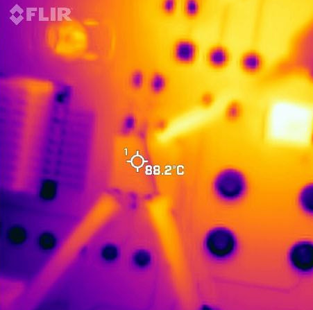
With 512 byte packets (CS=0 for 200us) it started to produce errors at +90C.
With 16 byte packets (CS=0 for 11us) I got no errors ever, and I tested it right up to +100C.

The above was without the very long CS=0 period between filling it and reading it out. During this period, the device should not be refreshing at all, and temperature dependent failures are expected:
With 512 byte packets and a 1000ms block on refresh, it started to produce errors at +50C.
With 512 byte packets and a 100ms block on refresh, it started to product errors at +70C.
The above is a totally unrealistic test because nobody will be deliberately blocking refresh by holding CS=0.

CS=1 for about 8us in all cases. That is probably important because clearly the chip starts the internal refresh as soon as it sees CS=1, and with the min CS=1 spec of just 50ns it must be pretty quick about it. It is reasonable to assume that the 50ns gives it time for just one refresh and as above debate shows, that adds up to some kind of normal DRAM refresh rate.

The fact that there is a measurable temperature dependency of the errors between CS=0 for 11us and 200us suggests that while the chip manages to squeeze in the initiation of a refresh in the 50ns CS=1 gap, it doesn't do the refresh cycles all that fast afterwards. I reckon it does them at a rate of about (order of magnitude) 1 every 1us.

Next I tested the hypothesis that reading more than 8192 (or 1024) consecutive locations does a full refresh. A test with a packet size of 8192 (CS=0 for 3ms) produces errors at around +70C. This is slightly worse than the 512-byte packet situation where it starts to fail at +90C. This is with a CS=1 time of around 8us as previously. Increasing the 8us to 100us does not change the +70C temperature, which is also interesting because it suggests that the chip is not grabbing that extra opportunity to squeeze in enough refresh cycles. Or maybe the temperature issue is not refresh related after all?

No matter how you shake it, the 8us number seems extremely conservative. Or maybe they are working on a really high chip temperature, produced by the maximum clock rates of 144MHz at a Tamb of +85C. In my product, running the RAM test all the time, the delta-T of the chip, relative to the PCB, is under 1K (1C).
« Last Edit: June 09, 2022, 08:56:49 pm by peter-h »
Z80 Z180 Z280 Z8 S8 8031 8051 H8/300 H8/500 80x86 90S1200 32F417
 
The following users thanked this post: PCB.Wiz

Online DavidAlfa

  • Super Contributor
  • ***
  • Posts: 5907
  • Country: es
Hah! The APS12808L-3OBM-BA provides 1us tCEM for ext. temp. range.
DDR octo-spi@133MHz will do 266bytes, but that time window is barely usable in simple spi and slower rates.
I guess the mcus will eventually support this natively, reducing the overhead and providing maximum efficiency.
« Last Edit: June 11, 2022, 01:42:20 pm by DavidAlfa »
Hantek DSO2x1x            Drive        FAQ          DON'T BUY HANTEK! (Aka HALF-MADE)
Stm32 Soldering FW      Forum      Github      Donate
 

Offline PCB.Wiz

  • Super Contributor
  • ***
  • Posts: 1542
  • Country: au
Next I tested the hypothesis that reading more than 8192 (or 1024) consecutive locations does a full refresh. A test with a packet size of 8192 (CS=0 for 3ms) produces errors at around +70C. This is slightly worse than the 512-byte packet situation where it starts to fail at +90C. This is with a CS=1 time of around 8us as previously.
Strange, that suggests you cannot actually get the theoretical equivalent of full refresh, by doing a full chip-wide (8192?) read ?  Maybe it needs other than 8192 ? ( addit: I see #34 mentions 16384 was always ok ? )


Increasing the 8us to 100us does not change the +70C temperature, which is also interesting because it suggests that the chip is not grabbing that extra opportunity to squeeze in enough refresh cycles.
Can you easily check Icc during CS=1 ?
I could never decide if the parts data implied it 
a) ran refresh during CS=1 (that implies a second on chip oscillator and needs the complexity of clock gating, and would have non zero Icc )
or
b) if they used the SCK to do refresh during the preamble of address load. There are quite a few clocks, where nothing happens inside the RAM array.
That means CS=1 time is not gaining anything.
« Last Edit: June 10, 2022, 04:49:47 am by PCB.Wiz »
 

Offline peter-hTopic starter

  • Super Contributor
  • ***
  • Posts: 3697
  • Country: gb
  • Doing electronics since the 1960s...
Quote
I guess the mcus will eventually support this natively

As I wrote before, I am damn sure the ESP32 doesn't do more than four bytes at a time.

Quote
Hah! The APS12808L-3OBM-BA provides 1us tCEM for ext. temp. range.

Typically of chinese parts (they probably ripped off the design from somebody else) they still don't explain why this is. Is it to give a more frequent CS=1 interval? I find that hard to believe because it cripples applications which want to transfer a lot of bytes but infrequently.

Quote
DDR octo-spi@133MHz will do 266bytes, but that time window is barely usable unusable in simple spi and slower rates.
I guess the mcus will eventually support this natively

Maybe but it uses up a lot of GPIO pins. And you still get a huge performance hit compared to normal RAM. Basically these chips are ok for a narrow range of applications where you want the 16 MB but don't care about the x10 to x100 slowdown. In most cases the application has to be specially designed to work with this chip even if the SPI is transparent. Same with my LY68L6400; one has to code it in specially, using it for buffering specific data.

Quote
that suggests you cannot actually get the theoretical equivalent of full refresh, by doing a full chip-wide (8192?) read ?  Maybe it needs other than 8192 ? ( addit: I see #34 mentions 16384 was always ok ? )

I can't find the mention of 16384 but I tested it. Like 8192, it still fails at +70C.
I also tested the refresh-by-access hypothesis with

Code: [Select]

spi_ram_cs(0);
osDelay (10000);  // 10 second refresh block
spi_ram_cs(1);

between filling it and reading it all back, and it fails 100% of the time. So quite bizzarely this chip does not refresh by accessing the memory array. I wonder how they achieved that ;) Don't normal DRAM chips do that? They always used to.

16384 is not really usable except to play with; +70C is too low.

IMHO, 512 is a good number. This fails at +90C. This would be OK for "normal" SPI usage where you are

- just using it as a data buffer, not running code out of it, etc
- not using a 100MHz+ SPI clock (I am using 21MHz; the max possible)
- product Tamb spec is not above +65C (+85C, even assuming negligible self heating, is a bit suspect because plastics start to go soft)

Quote
Can you easily check Icc during CS=1 ?
I could never decide if the parts data implied it
a) ran refresh during CS=1 (that implies a second on chip oscillator and needs the complexity of clock gating, and would have non zero Icc )
or
b) if they used the SCK to do refresh during the preamble of address load. There are quite a few clocks, where nothing happens inside the RAM array.
That means CS=1 time is not gaining anything.

I did wonder about Icc spikes during CS=1, to test the refresh hypothesis. Well, they obviously do have an internal oscillator for this, because the chip has to hold data with no SPI activity.

Yes, with the SPI protocol - 4 bytes of overhead, 5 bytes with the faster rates - there is ample time for refresh. So they have much more than the 50ns min CS=1 time.

We are stuck with a data sheet written by monkeys, or written to not reveal who the design is stolen from :)

The two images show the timings with 512 bytes and with 16 bytes. On the latter you can see the 4 byte header overhead. I could optimise the code (there is a lot one can do e.g. set up one's data buffer to have the 4 byte header in front of it, so just one DMA transfer is needed, or do the DMA code inline so the DMA pointers don't need reloading, etc) but for the 512 byte case this is pointless.
« Last Edit: June 10, 2022, 06:22:39 am by peter-h »
Z80 Z180 Z280 Z8 S8 8031 8051 H8/300 H8/500 80x86 90S1200 32F417
 

Offline PCB.Wiz

  • Super Contributor
  • ***
  • Posts: 1542
  • Country: au

I can't find the mention of 16384 but I tested it. Like 8192, it still fails at +70C.
I also tested the refresh-by-access hypothesis with

Code: [Select]

spi_ram_cs(0);
osDelay (10000);  // 10 second refresh block
spi_ram_cs(1);

between filling it and reading it all back, and it fails 100% of the time. So quite bizzarely this chip does not refresh by accessing the memory array. I wonder how they achieved that ;) Don't normal DRAM chips do that? They always used to.

16384 is not really usable except to play with; +70C is too low.
I'm not quite following this test ?
10s confirms it is volatile DRAM, but to test refresh-by-access, you would need to scan the DRAM inside the refresh time ( ISTR seeing 64ms whole chip times somewhere ? )  and squeeze all other times to try to exclude any auto-refresh.
 

Offline peter-hTopic starter

  • Super Contributor
  • ***
  • Posts: 3697
  • Country: gb
  • Doing electronics since the 1960s...
Ah yes you are totally right. I would need to fill it up, then keep reading say 16384 locations, with 64ms gaps with CS=0.

But I am sure it will pass that test. It already passes a 16k fill, a 1 second wait with CS=0, and then reading it all back.

I tried to see if holding CS=0 for 64ms at a time, followed by a read of x addresses, for 6.4 seconds, will produce corrupted data

Code: [Select]
for (int i=0;i<100; i++)
{
kde_spi_ram_cs(0);
osDelay (64);
kde_spi_ram_cs(1);
SPI_RAM_read(0,(uint8_t*)bufc,pkt);
}

and it does not. So it appears that the device does get refreshed by reading. But... the problem is that this works fine for all kinds of x values. I would have expected it to fail for x < 1024, or x < 8192, but even x=512 and x=16 work fine. So somehow the device is managing to sneak in enough refreshes. There are no errors even at elevated temperatures.

Now I am trying to identify the device presence, at product startup. Apart from some test data, it looks like the Read ID would be a good way. Counting the bits in fig 12.4, 0 to 103, it looks like 9 bytes are read, including the OD 5D. I am seeing the 0D 5D and the rest looks random except for a CR at the end. This is data from two different devices


So just one byte differs. These came out of a strip of 10, so it looks like a serial number. But it could be some device property, so maybe not unique.
« Last Edit: June 10, 2022, 01:59:33 pm by peter-h »
Z80 Z180 Z280 Z8 S8 8031 8051 H8/300 H8/500 80x86 90S1200 32F417
 

Offline woofy

  • Frequent Contributor
  • **
  • Posts: 334
  • Country: gb
    • Woofys Place
I would guess its a UID, 48 bits is a common length for that, but I would check all 10 devices anyway.

What a wonderful data sheet  |O

Offline peter-hTopic starter

  • Super Contributor
  • ***
  • Posts: 3697
  • Country: gb
  • Doing electronics since the 1960s...
Some devices have a randomised ID, while some have a very non-random ID which could just be 1 bit away from the next one (but they still guarantee all are unique), while some have a huge number which is incrementing.

I suspect the last one is what this device does.

I am using only the first two bytes, whose values are documented in the data sheet, to detect device presence. There is no point in using the other 7 bytes given that this is an optional feature in the product.

It's actually quite a challenge to use this stuff to form a normal looking serial number. You have to hash it into something which can be printed out on a label and not be too long, and accept it won't be incrementing. I suppose one could use it to form an ETH Mac # ;) ;)

BTW I also found another issue with this "CS=0 maximum" business: in an RTOS environment, it can be easy to stretch the CE=0 time to some large figure if a higher priority task is running, and then you do get data corruption, as one might expect. The longest packet I tested with was 16384 which transfers in about 6ms, and I found that if one goes well beyond that, say 15ms, the data does get corrupted. Not surprising since the data sheet says 8us max :) but still a useful data point.
« Last Edit: June 11, 2022, 08:43:12 am by peter-h »
Z80 Z180 Z280 Z8 S8 8031 8051 H8/300 H8/500 80x86 90S1200 32F417
 

Online DavidAlfa

  • Super Contributor
  • ***
  • Posts: 5907
  • Country: es
Check the tkm32f499... 128pin, 240MHz, Cortex-M4, embedding 8MB SDRAM.
Hantek DSO2x1x            Drive        FAQ          DON'T BUY HANTEK! (Aka HALF-MADE)
Stm32 Soldering FW      Forum      Github      Donate
 

Online hans

  • Super Contributor
  • ***
  • Posts: 1640
  • Country: nl
BTW I also found another issue with this "CS=0 maximum" business: in an RTOS environment, it can be easy to stretch the CE=0 time to some large figure if a higher priority task is running, and then you do get data corruption, as one might expect. The longest packet I tested with was 16384 which transfers in about 6ms, and I found that if one goes well beyond that, say 15ms, the data does get corrupted. Not surprising since the data sheet says 8us max :) but still a useful data point.

If you use DMA SPI, you could use the transfer complete interrupt to clear chip select active.
Otherwise, if you use small bursts of 8us, you maybe block the OS from context switching if this is a low priority task, but that's kind of a messy hack.

But like said, it's not recommended to go beyond the 8us maximum to have proper function over temperature. If you have hot air, I would be interested to hear what happens if you turn it on at 70C , and point it to the PSRAM chip while doing the same test. I bet data corruption would take place with a shorter CS interval.
Maybe I actually do this test -out of curiosity- with the HyperRAM chips I've got. I've got them talking properly over OCTOSPI and can adhere to the 4us limit by hardware, but it's also possible to configure a high amount of refresh cycles and stretch it far beyond 4us.

Maybe you could still stretch CS if you don't need the full temperature range of operation, but IMO it's getting in the sketchy territory where I would use large margins to make sure things a 3-sigma or greater population spread should still work. But it's all second guessing when you don't have hard data on how fast the SDRAM cells discharge for a specific temperature.
 

Offline peter-hTopic starter

  • Super Contributor
  • ***
  • Posts: 3697
  • Country: gb
  • Doing electronics since the 1960s...
I did the temp tests - see posts above. I would conclude that there is a continuous spectrum of temperature dependency, from CE=0 being 8us, through longer CE=0 values, and at temps below about +40C there are no failures at any CE=0 period below about 1 second.

One could measure this and plot it.

It also seems obvious that the 8us spec, and slightly bigger values e.g. 20-50us, correspond to a pretty extreme set of conditions (probably assisted by strong chip self-heating) as I wrote above. For example the data sheet gives the max Icc as 40mA which at 3.3V is 132mW and looking at some examples online for thermal resistance chip to PCB (about 70K/W, junction to PCB, for non high power SO-8 devices) this translates to a temp rise of 10C, yet my thermal imaging shows < 1C rise in my application which is a continuous test but at 21MHz instead of 100+ MHz.

The CE=0 lenghtening is easily fixed by disabling the event interrupt which is causing this, during the packet. That is the USB interrupt. I posted about this before. During FLASH FS write it can be 16ms. During a FLASH FS read it is only 200us.

So far I have tested just two chips and the 2nd one I am unable to make fail, by heating with hot air. The tests on the first chip were done by heating its package directly with a soldering iron until it started to fail and then its temperature was read off on the IR imager. Obviously I will do more tests on that chip.
« Last Edit: June 11, 2022, 05:24:51 pm by peter-h »
Z80 Z180 Z280 Z8 S8 8031 8051 H8/300 H8/500 80x86 90S1200 32F417
 

Offline peter-hTopic starter

  • Super Contributor
  • ***
  • Posts: 3697
  • Country: gb
  • Doing electronics since the 1960s...
I did a few more temp tests, this time on another chip. Packet size in bytes, failure temp in degC

16384   70
512   70
256   80
128   95
64   115

I didn't go above 115C.

The transfers are DMA, 21MHz. A 512 byte packet has CS=0 for 200us.

Like I said before, the max CS=0 of 8us to be "real" would need some pretty extreme conditions. And at 21MHz, running the test solidly, the top of the chip is the same temp as the PCB, within the resolution of the IR sensor.


The hot bit in the bottom left has a U-BLOX GPS module on the other side of the PCB, drawing a few tens of mA.

« Last Edit: June 15, 2022, 03:51:17 pm by peter-h »
Z80 Z180 Z280 Z8 S8 8031 8051 H8/300 H8/500 80x86 90S1200 32F417
 

Online DavidAlfa

  • Super Contributor
  • ***
  • Posts: 5907
  • Country: es
Although improvable, you could try contacting them for more info.
Hantek DSO2x1x            Drive        FAQ          DON'T BUY HANTEK! (Aka HALF-MADE)
Stm32 Soldering FW      Forum      Github      Donate
 

Offline iMo

  • Super Contributor
  • ***
  • Posts: 4784
  • Country: pm
  • It's important to try new things..
A decade back I messed with ISSI IS66_something 4Mx16 PSRAM (48pin BGA). I built a xilinx based controller to make an 8bit serial 8MB "octoram" out of it :phew:. We used to use it with arduinos and with the pic32MX as swap file and ramdisk (retrobsd project). It also had 8us CE max, thus it seems to me that it is the same dram core used for your SPI chip as well. It had several control registers, afaik in one of the regs you could set the temperature for temperature compensated refresh (4 temperature profiles). Doublecheck with your chip, perhaps it may help you somehow.
« Last Edit: June 14, 2022, 07:02:08 pm by imo »
 

Offline peter-hTopic starter

  • Super Contributor
  • ***
  • Posts: 3697
  • Country: gb
  • Doing electronics since the 1960s...
The data sheet has nothing (see above) and I would think that any DRAM chip config registers would be inaccessible once the devices are placed behind an SPI or QSPI controller.

Actually it is an interesting Q for these devices which apparently contain two DRAM chips: do the DRAM chips have an SPI+QSPI controller, which is ignored if the DRAM is packaged with a parallel interface (TQFP,BGA etc) for a memory module, but can be activated for packaging in an SO-8? It would also need a provision for connecting multiple DRAM chips together. Otherwise, these SO-8 packages would have to contain three chips: the two DRAMs and the SPI+QSPI controller. And a large number of bonding wires.

Really interesting stuff, but unsurprising since refresh requirements are heavily temp dependent.
« Last Edit: June 15, 2022, 04:13:45 pm by peter-h »
Z80 Z180 Z280 Z8 S8 8031 8051 H8/300 H8/500 80x86 90S1200 32F417
 

Offline peter-hTopic starter

  • Super Contributor
  • ***
  • Posts: 3697
  • Country: gb
  • Doing electronics since the 1960s...
I did some final tests on this chip, to explore the hypothesis that if after a long packet you don't access it for a bit, it will have enough time to refresh the entire chip.

The results are very interesting, and will solve the issue in the right applications.

With a 1024 byte packet (400us CS=0) one needs 50us of CS=1 to avoid errors at +105C (not tested higher)
With a 8192 byte packet (3200us CS=0) one needs 100us of CS=1 to avoid errors at +80C (not tested higher).
With a 16384 byte packet (6400us CS=0) one needs 300us of CS=1 to avoid errors at +80C (not tested higher).

Contrast this with the CS=0 spec of 8us max :)

Fairly obviously the internal refresh is fairly quick.

At packet sizes like 1024 bytes it is rock solid at > 100C.

So one needs just a fairly short CS=1 time to make a complete nonsense of the 8us spec.

This suggests that my earlier view may be right: the 8us is based on CS=1 being the shortest possible time per spec: just 50ns. With just 50ns, the internal refresh controller manages to do just one row refresh cycle per transaction, and this is the huge overriding factor in the 8us spec. As someone pointed out earlier, 8us * 8192 = 65ms which is close to a DRAM whole-device (8192 rows) refresh period. So this all hangs together now. The 8us is probably based on this simple calculation, together with the assumption that the host will be thrashing the chip solidly, with no time gaps.

In addition, the 8us spec will be based temperature-wise on the max SPI clock of 100MHz+ (I am running at 21MHz and with negligible chip self-heating) and max ambient of +85C.

Why do they cripple the spec so badly? They could say that the 8us becomes say 200us if CS=1 for 50us. But they don't; the data sheet is junk.

« Last Edit: June 24, 2022, 06:21:08 pm by peter-h »
Z80 Z180 Z280 Z8 S8 8031 8051 H8/300 H8/500 80x86 90S1200 32F417


Share me

Digg  Facebook  SlashDot  Delicious  Technorati  Twitter  Google  Yahoo
Smf