Yes... but it depends on what kind of bga you're talking about.
Pitch, total balls, ballout pattern, total ball usage all affect what pcb specs you will need.
Design considerations:
Devices designed for low cost embedded applications (say, TI arm cpus) have pinouts optimized for breakout on 4 layer and with some effort, even 2 layers.
These devices will have voids in the ballouts to allow you to place bypass caps and breakout routing. For IO constrained applications like FPGAs you will need 4 layer and go up from there.
For proper bga fanout you will want to be able to put a via in between the ball pads. The deeper the distance to the center of the bga, the more layers you need to break it out.

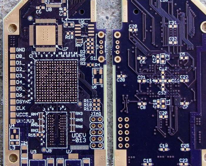
Here is a pcb I did with 6mil trace/space and 13mil drills. It is sufficient for a modestly broken out 1mm pitch BGA. 0.8mm, not so much. The pad land diameter affects the height the package will sit at, and also the size and geometry of the resulting joint. I used non-soldermask defined pads (NSMD). This allows the solder to grab around the edges of the copper etching.
Assembly considerations:
Reflowing the bga is a process in itself. You can't just blast heat on it. The requirements are: preheat the entire board to the first step of the bga reflow profile. Then apply local heat as evenly as possible to the bga solder balls. That's the rough view.
You can reflow smaller (<256) bgas that are MONOLITHIC flip chip (that is, solid black square) with a preheat and a hot air station. Substrate-mounted chips do NOT like this, you will warp the substrate and ruin the chip. The bigger the package, the lower maximum temperature the package can handle. Always look at the part datasheet for soldering guidelines.
I use a $600 convection oven with shielded elements and local thermocouple. You will want good, even heat that is well monitored. You can fudge dry runs to get the results you need, but it's hopeless if you can't read the results.
Profile for a large board with 484pin 1.0mm bga:
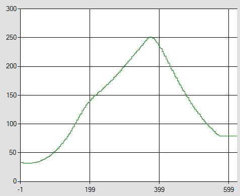
Important parameters are rate of temperature ramp up, length of pre-heat (which is almost zero here), length of time spent above liquidus (solder molten temperature) and cooloff timing.
There is lots more info than I have room to write about here.
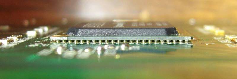
Heres the result, pardon the glare, it's hard to take pictures at such an extreme angle.
All BGAs nowadays come preballed with leadfree balls. Melting point as about 218 C. I mount the bga first on empty pcb, then go back and hand solder everything else with leaded.
You can either use a paste stencil and deposit solder paste as your means of "starting" the connection, or just flux. Laying down paste is a better idea but if you don't have a stencil, you can flux the pcb pads, lay down the BGA and let'er rip. Alignment is a non-issue. You can be off the bga pads by 49% and it still works. Rotated chip? No problem.
Flux-only method means you need a FLAT pad surface. HASL is unusable. I use ENIG as you can see above. Immersion silver would also work.
Flux type is important. You don't want the flux to completely burn off and be useless by the time the balls start melting. DO NOT use water soluble or no-clean flux. You will have no more vias underneath your BGA. Always tent vias with soldermask. I use MG Chemicals ROSIN flux pen. It may not be the best choice but it works. Pastey/less runny flux is better.
Here is one last pic.
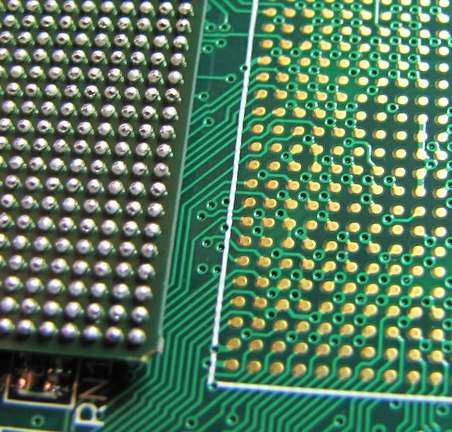
You can see the small soldermask allowance around the pad for NSMD pads. Keep your annular ring on vias as big as allowable. You can see the drill wander on some of the holes here. Always neck down the dogbones to 2/3 or less of the pad diameter to keep the ball shape from becoming abnormal and stressing the joint. That fpga on the left shows what you will get from the factory.
One last thing: You MUST observe moisture rules on the parts. Don't remove parts from the bags with silica gel until you are ready to reflow. Moisture will work into the porous bga package and the water pockets can popcorn and cause unseen damage. JEDEC procedure for removing latent moisture is something like 125 C for 12 hours. Same goes for the pcbs themselves.
If you have more specific questions let me know. There is a lot of stuff I probably missed.


