Author Topic: Coefficient of Thermal Expansion and PCB curvature following soldering  (Read 8613 times)

0 Members and 1 Guest are viewing this topic.

Offline .o:0|O|0:o.Topic starter

  • Regular Contributor
  • *
  • Posts: 131
  • Where is Higgs Boson?
I have this ongoing project (not really deserving of the name as it has taken 4 years so far) to make one of those Christmas light nets which can be programmed to display text/graphics. Rather than use a standard array, I thought it might be interesting to use an interleaved quincunx array, which in theory gives double the vertical and horizontal resolution. This is a prototype I made to play around with rather than having a huge wall sized thing.

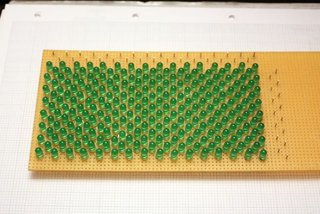
Oh boy, that lot took some soldering!
When a board is heavily populated or reworked (say with the help of a hot air gun.....), you often find that the board curves. Two questions:

1) Why does it curve? Is this due to the copper side being unable to return to its original dimensions due to the introduction of added material within the copper plane while heated? Is there some change in the epoxy layer? It seems to happen when many components are (re-) soldered.

2) How do you prevent it? Would a brace/frame during the soldering prevent this effect from taking place?

.o:0|O|0:o.

Were you intending to make a new topic or something?

I think a board warps because the thermal expansion rate of materials on the board is different. When you only heat up one part of the board it'll warp in that area. That said, I haven't ever had problems with this and I've applied way too much heat to FR-4's before. Is your board particularly thin?

You can try using a pre-heater. Either a skillet or hot plate or one of the expensive dedicated PCB preheater units. It bakes the entire board at a nice temperature so that there's less thermal shock when you solder.

I just wanted a reasonable explanation to a question relating to a slight curve I noticed in the prototyping board above, which is barely noticeable in this case, but which I have seen many times when working on various boards to a greater extent. So, in answer to your first question: not really. However, I have removed my post from the other thread to this one to avoid hijacking and irritating people. Then if people have any ideas they can comment.

My question was deeper, but not very. I am familiar with thermal expansion coefficients being different for different materials - bimetals use the principle to great effect. However, bimetals (unless they have peculiar properties like Nitinol) return to their former size and shape once allowed to cool down. The copper on that and on other boards should return to its former size and near lack of curvature, yet it often doesn't. Admittedly, the question barely applies to the board shown, but it reminded me of something I worked on recently.

.o:0|O|0:o.
« Last Edit: November 02, 2010, 05:55:29 pm by .o:0|O|0:o. »
 

Offline .o:0|O|0:o.Topic starter

  • Regular Contributor
  • *
  • Posts: 131
  • Where is Higgs Boson?
Re: Coefficient of Thermal Expansion and PCB curvature following soldering
« Reply #1 on: November 02, 2010, 05:58:18 pm »
Apparently the correct term for this phenomenon is "Thermal Warpage". See http://apl.aip.org/resource/1/applab/v81/i21/p4079_s1?isAuthorized=no

.o:0|O|0:o.
 

Offline FreeThinker

  • Frequent Contributor
  • **
  • Posts: 791
  • Country: england
  • Truth through Thought
Re: Coefficient of Thermal Expansion and PCB curvature following soldering
« Reply #2 on: November 02, 2010, 07:47:33 pm »
Just a thought but could it be due to thermal creep? Ie if the board is multilayer could it not be due to the layers cooling at different rates and the adhesive cooling before the layers have contracted fully?This could also cause bending on a single layer board if large areas of copper cooled slower than the substrate and the adhesive cooled on the expanded copper which then cooled and shrunk bending the board.
Machines were mice and Men were lions once upon a time, but now that it's the opposite it's twice upon a time.
MOONDOG
 

Offline .o:0|O|0:o.Topic starter

  • Regular Contributor
  • *
  • Posts: 131
  • Where is Higgs Boson?
Re: Coefficient of Thermal Expansion and PCB curvature following soldering
« Reply #3 on: November 03, 2010, 02:12:50 am »
Just a thought but could it be due to thermal creep? Ie if the board is multilayer could it not be due to the layers cooling at different rates and the adhesive cooling before the layers have contracted fully?This could also cause bending on a single layer board if large areas of copper cooled slower than the substrate and the adhesive cooled on the expanded copper which then cooled and shrunk bending the board.

Yes, that would make sense. I also read that the copper sheets have a slight curvature to begin with because they are pressed with large heavy rollers (before being cut to smaller rectangles) ....which results in large rolls of copper sheeting. Perhaps there is a tendency for the metal to also have some shape memory, but I think you are right.
When reheating old solder joints through multiple layered boards you sometimes hear a little "snapping" sound as though there is a difference in heating -- it can be very concerning. I wonder if a brace or frame would prevent the effect you described. It is also a concern for when the boards undergo temperature changes while in use.

.o:0|O|0:o.
 

Offline Mechatrommer

  • Super Contributor
  • ***
  • Posts: 11630
  • Country: my
  • reassessing directives...
Re: Coefficient of Thermal Expansion and PCB curvature following soldering
« Reply #4 on: November 03, 2010, 06:22:42 am »
its something got to do with thermo machanical thing. IMO
Nature: Evolution and the Illusion of Randomness (Stephen L. Talbott): Its now indisputable that... organisms “expertise” contextualizes its genome, and its nonsense to say that these powers are under the control of the genome being contextualized - Barbara McClintock
 

Offline FreeThinker

  • Frequent Contributor
  • **
  • Posts: 791
  • Country: england
  • Truth through Thought
Re: Coefficient of Thermal Expansion and PCB curvature following soldering
« Reply #5 on: November 03, 2010, 11:16:55 am »
In my (limited) experience of industrial reflow machines the pcbs go through a temperature profile of slow heating , wave or bath solder then controlled cooling in order to mimimise  the effects of warping (among other things) lots of thermal stresses going on and you need to try to even things out.The larger the board the worse it is.The temperature profiles were adjusted to meet certain parameters at known points in the machine the ideal was to evenly heat every thing to just below the soldering temp so that when it went into the bath the thermal shock was minimized.Then a controlled cooling took place to allow any stresses to even out.It's a bit of a black art to get it just right, ambient temperature, filters being clean etc all playing a big part.Hand soldering can introduce local area stresses which can cause failures, not an option when the unit is the control system for airbag deployment.
Machines were mice and Men were lions once upon a time, but now that it's the opposite it's twice upon a time.
MOONDOG
 

Offline sonicj

  • Frequent Contributor
  • **
  • Posts: 756
  • Country: us
  • updata successed!
Re: Coefficient of Thermal Expansion and PCB curvature following soldering
« Reply #6 on: November 03, 2010, 12:00:54 pm »
i wonder if, when soldering a board like above, using a diagonal pattern similar to tightening lugnuts on a wheel could reduce this type of warping???

ever notice how solder wick curls up? i hate that!
-sj
 

Offline FreeThinker

  • Frequent Contributor
  • **
  • Posts: 791
  • Country: england
  • Truth through Thought
Re: Coefficient of Thermal Expansion and PCB curvature following soldering
« Reply #7 on: November 03, 2010, 12:25:41 pm »
i wonder if, when soldering a board like above, using a diagonal pattern similar to tightening lugnuts on a wheel could reduce this type of warping???

ever notice how solder wick curls up? i hate that!
-sj
When hand soldering it is a good idea to only work small areas of the board at a time moving to cool areas every 30 seconds or so to avoid overheating.The reason solder wick curls is that solder and copper have different coefficients of expansion and therefore cool at different rates, the solder cools quicker and solidifies while the copper is still expanded.This extra trapped length has to go somewhere so hence the curl.
Machines were mice and Men were lions once upon a time, but now that it's the opposite it's twice upon a time.
MOONDOG
 

Offline TechGuy

  • Regular Contributor
  • *
  • Posts: 79
Re: Coefficient of Thermal Expansion and PCB curvature following soldering
« Reply #8 on: November 03, 2010, 05:09:09 pm »
Thermal warpage occurs when an object is heated unevenly. I am sure we all experienced this with warped brake rotors on your car. The breakpads heat up the rotor. if one part of the rotor is cooler much quicker than another part, the rotor becomes warped.

There is also another phenomenon caused when welding, brazing or soldering. As a solder joint cools it pulls the pieces closer, which creates tension. Since your preferated board has a large number of connections close together it may be pulling on the solder side, causing warpage. The only way to avoid this warpage is to securely clamp the board so it cannot warp when the solder joints cool, which of course is difficult with all of the LEDs creating a non-flat surface.

FWIW: it would be far easier to build your device using surface mount LEDs instead of through hole LEDs. Using surface mount you can place all of the devices and use reflow to solder them all at once. I suspect that a similar PCB using surface mount with a stecil would take you a couple of hours to place all those LEDs and about 10 minutes to reflow solder them. I suspect that your preferated board took at least a 20 to 40 hours to solder.


Offline Zad

  • Super Contributor
  • ***
  • Posts: 1013
  • Country: gb
    • Digital Wizardry, Analogue Alchemy, Software Sorcery
Re: Coefficient of Thermal Expansion and PCB curvature following soldering
« Reply #9 on: November 03, 2010, 11:56:13 pm »
To throw more fuel onto the fire, here is the reverse side of the Perfboard (it isn't PCB). The warping must be generated in the manufacturing process as they roll the board. At worst it is only around 3mm from planar, and easy enough to straighten out by hand. Note that there is only insulation on the left (where I started). I calculated the time it was taking to sleeve the wires and realised it would take me days to finish, and the chance of row and colum wires touching was minimal. I should say that it is in no way a soldering demo piece, just a proof of concept and good enough to do what I wanted it to. After being lying around for several years it is slightly battered, but there are no shorts. It really is simpler in '3D' than is appears on the photo. Clearance between horizontal and vertical wires is 6mm. I started by using SMD LEDs, but after mounting 3 of them I started to fear for my sanity and went back to cheap low efficiency PTH ones.


Offline .o:0|O|0:o.Topic starter

  • Regular Contributor
  • *
  • Posts: 131
  • Where is Higgs Boson?
Re: Coefficient of Thermal Expansion and PCB curvature following soldering
« Reply #10 on: November 04, 2010, 02:31:11 pm »
....That explains why the board was surprisingly flat. That is I good strategy if eventually you decide to re-use the LEDs for something else and if one goes out maybe it is easier to replace (unless in heating the wire neighbouring ones come loose....). You deserve a medal for patience!

I think at some point I am going to measure a few sticks of aluminium, drill a hole at the ends and secure them along the edges of the board while I solder. With discreet components I tend to solder as many of the leads at once (I think I picked that habit up at some point because of solder fumes), so it is inevitable that the board will heat up quickly on one side. Maybe a stencil, solder paste, surface mount components and an air gun would give better results as suggested -- something to try.

.o:0|O|0:o.


Share me

Digg  Facebook  SlashDot  Delicious  Technorati  Twitter  Google  Yahoo
Smf