Author Topic: Compensation methods in current sink circuits  (Read 21129 times)

0 Members and 1 Guest are viewing this topic.

Offline thexenoTopic starter

  • Regular Contributor
  • *
  • Posts: 83
  • Country: it
  • Just another EE
    • Personal website
Re: Compensation methods in current sink circuits
« Reply #25 on: January 03, 2016, 10:15:12 pm »

where is your circuit? or which circuit from the above are you referring to ? Post the spice asc file of your circuit and it will be much easier to help you.
So this is telling you the gate pole has moved down in freq because of larger input capacitance (Ciss) of the irli630 fet.


If I modify the schematic by adding R1 and C1:


The control loop becomes:


Regards,

Jay_Diddy_B

Kevin, that is my circuit with the new mosfet (IRLI630GPBF). I don't have a full simulation because I don't know what is an equivalent mosfet to mine, and IRLI630GPBF  is not present in LT-Spice.

Did I answered to you?

Let's add that the compensation used is 100ohm and 10nF, because with the BUZ70 the one used in the simulation above did not remove the oscillations. I don't know if this is somehow related to the fact that with the IRLI630GPBF and a tank capacitor on Vdd the stability is achieved.

Happy new year :)

Offline thexenoTopic starter

  • Regular Contributor
  • *
  • Posts: 83
  • Country: it
  • Just another EE
    • Personal website
Re: Compensation methods in current sink circuits
« Reply #26 on: February 14, 2016, 10:16:41 am »
Hi! It's been a while, now I can appreciate more your answers. I refreshed my mind!

I read again all the topic, the Dynamic electronic load project, a couple of books...


Then draw up the RC low pass formed from gate + open loop impedance driving it (can measure it closed-loop, take it from datasheet if specified, sometimes from equivalent schematic, when the emitter resistors' values are specified these are the dominant impedance for the output impedance). Draw your feedback network on the bode sheet. Add the curves. Tadaa, loop gain bode plot. Of course only an approximation. When the data collected is conclusive a good one, good enough for determining compensation network. A nice exercise for any EE student.


I still have troubles in discerning the concept of loop gain with the feedback network. In other words, what do you mean with:
Draw your feedback network on the bode sheet. Add the curves. Tadaa, loop gain bode plot.
Why does not the feedback network is actually the loop gain?

Before answering better to everyone, I'd like to say that the cirucit is completely stable, or  it seems to be, with compensation used with the BUZ70 and 100uF cap on power rails (100uF because I had this one only...).

Answering to myself, this was a counter measure to the lead inductance present on the drain. Demonstrating that the oscillation was due to inductance and not at all (right?) with the lower pole in the feedback due to the fat MOSFET.
I am still in the dark to know how a parasitic inductance and any stuff placed on drain can caffect the system. Does it depends on the transconductance gain of the mosfet, which contains the Rd/Rs terms under the degenerated common source configuration?

Personal note: I am a bit unsatisfied with this circuit because I started it as an exercise to try to find the pole, compensate, draw pole and zeros on complex plane ecc, but I almost instantly being stucked by the fact that the main pole is due to a parameter difficult to know: the Rout of the op-amp.
« Last Edit: February 14, 2016, 10:25:15 am by thexeno »
 

Offline dom0

  • Super Contributor
  • ***
  • Posts: 1483
  • Country: 00
Re: Compensation methods in current sink circuits
« Reply #27 on: February 14, 2016, 11:00:53 am »
Quote
Why does not the feedback network is actually the loop gain?

Loop gain is the gain a disturbance experiences when it "travels around the loop once". So you need to take amplifier transfer function into account. That's why you need to add the curves of the op amp, the feedback network and that low pass. This is then the loop gain.
,
 

Offline thexenoTopic starter

  • Regular Contributor
  • *
  • Posts: 83
  • Country: it
  • Just another EE
    • Personal website
Re: Compensation methods in current sink circuits
« Reply #28 on: February 14, 2016, 03:00:31 pm »
Loop gain is the gain a disturbance experiences when it "travels around the loop once". So you need to take amplifier transfer function into account. That's why you need to add the curves of the op amp, the feedback network and that low pass. This is then the loop gain.

I'd like to proceed in this way, like learned at university for simpler and famous configurations.  Here seems not possible to find the transfer function of the feedback, mainly because the more important pole depends on opamp's Rout.

I tried here few calculations and assumptions, that could be wrong.

« Last Edit: February 14, 2016, 04:00:44 pm by thexeno »
 

Offline thexenoTopic starter

  • Regular Contributor
  • *
  • Posts: 83
  • Country: it
  • Just another EE
    • Personal website
Re: Compensation methods in current sink circuits
« Reply #29 on: February 14, 2016, 11:31:10 pm »
Some news and results.

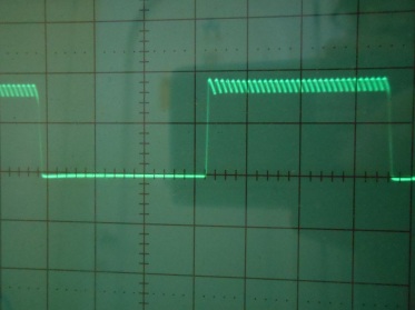
This is the real circuit, with BUZ70 with no compensation, Val = 8V for opamp and MOS:
 

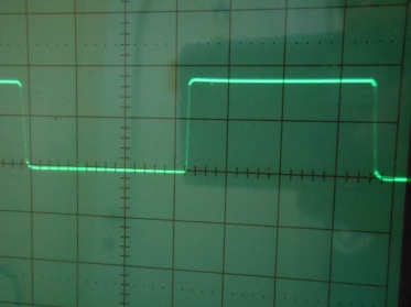
and inserting C=10nF, R=100ohm became:


The circuit was made on a 2layer PCB:


The blue resistor and the cap are the compensations. The others are pulldown on opamp input and the sense resistor, which is 4.7ohm. The MOSFET is BUZ70. I don't know why, but using 1000ohm resistor and 1nF will oscillate even more.

Now, with a new circuit which uses the "fatter" MOSFET IRLI630, uses also a resistor of 0.47ohm because the input also is 10 times lower. I don't have screens of the oscillations, but here what happens:

with the compensation like with the BUZ70, does not work, it is very noisy at 12V and oscillate up to saturation under 12V.
Inserting a 100uF electrolytic cap on Val, works well at 12V, became noisy at 5V and at 3.3V there is a ringing even greater than the one in picture before, at around 100kHz.

Then I tried with pole-zero compensation at 100kHz (between + and - of opamp), changes only a bit. Increasing with dominant pole by putting R=200ohm and not using zero-pole, therefore around 80MHz, it does not change anything. Using both solutions make the condition worst. I know, the inductance could be present on voltage lines, and the power supply is a PC's PSU, noisy, but my control loop is somewhat still unstable.

The requirement I'm looking for is high speed (between 150 and 200kHz at least) and a current precision which can be inside 5%.

Here in this forum are supported also projects, if I can be helped to going out from this stuck condition, I can start a new topic about it, and provide updates, if it worth. It is a 4 colour lamp, driven with 4 PWM channels from a micro, which I'd like to make in switching version (I am currently working on it) and a linear one, which could be used to modulate signals (here why the precision and frequency initial requirements).


Share me

Digg  Facebook  SlashDot  Delicious  Technorati  Twitter  Google  Yahoo
Smf