Author Topic: DACs - die pictures  (Read 24598 times)

0 Members and 1 Guest are viewing this topic.

Offline NoopyTopic starter

  • Super Contributor
  • ***
  • Posts: 1734
  • Country: de
    • Richis-Lab
DACs - die pictures
« on: April 04, 2020, 07:50:15 pm »

It seems that I have to create a DAC-topic.  ;D


Let´s start with the Burr Brown DAC709!


"U.K."  :-+


The datasheet gives you a lot of specifications:

Linearity Error: +/- 0,0015 %
Differential Linearity Error: +/- 0,003 %
Gain Error: +/- 0,07 %
Zero Error: +/- 0,05 %
Power Supply Sensitivity Vcc: +/- 0,0015 %/%Vcc
Power Supply Sensitivity Vdd: +/- 0,0001 %/%Vdd

Total Error Over Temp Range: +/- 0,08 %
Total Full Scale Drift: +/- 10 ppm/°C
Gain Drift: +/- 10 ppm/°C
Zero Drift: +/- 2,5 ppm/°C
Differential Linearity Drift: max + 0,009 / - 0,006 %
Linearity Error: max +/- 0,006 %

Settling Time (to +/-0,003%; voltage output): 4 µs
Slew Rate: 10 V/µs
Settling Time (to +/-0,003%; current output in 10Ω to 100Ω): 350 ns


BB used two dies so they didn´t have to integrate the logic on the same die as the analog part which probably would have degraded the performance of the analog part.
BTW: The Package has two interconnection layers.


I think BB was able to configure the logic die so it acts as a DAC707, a DAC708 or a DAC709.
The two bondwires connected over an isolated square are promising candidates.


That´s an big old gatearray!  :-/O


Nice test structures!  :-+


The DAC itself.


Resistor, Laser, Resistor, Laser, Resistor, Laser,...  ;D


Buried zener! Yeah!  ;D


Some more pictures here:

https://richis-lab.de/DAC01.htm


Offline ali_asadzadeh

  • Super Contributor
  • ***
  • Posts: 1905
  • Country: ca
Re: DACs - die pictures
« Reply #1 on: April 04, 2020, 08:09:11 pm »
Nice, pictures! :-+
ASiDesigner, Stands for Application specific intelligent devices
I'm a Digital Expert from 8-bits to 64-bits
 

Offline Wimberleytech

  • Super Contributor
  • ***
  • Posts: 1133
  • Country: us
Re: DACs - die pictures
« Reply #2 on: April 04, 2020, 11:24:50 pm »
The test structure brings back memories.  I used to routinely put those on my chips in the very early days. I never did field transistors, however.  Here is one from circa 1985.
 

Offline Wimberleytech

  • Super Contributor
  • ***
  • Posts: 1133
  • Country: us
Re: DACs - die pictures
« Reply #3 on: April 04, 2020, 11:27:38 pm »
And this from '79
 

Offline NoopyTopic starter

  • Super Contributor
  • ***
  • Posts: 1734
  • Country: de
    • Richis-Lab
Re: DACs - die pictures
« Reply #4 on: April 05, 2020, 06:52:19 am »
Such test structures are often very interesting.
I was surpriesed how many test structures they have put on the gatearray!

Online Miyuki

  • Frequent Contributor
  • **
  • Posts: 905
  • Country: cz
    • Me on youtube
Re: DACs - die pictures
« Reply #5 on: April 05, 2020, 10:16:15 am »
I wonder is today chips also with this test structures ?
And are they used mainly in first tuning of manufacture - like all that diffusion times and temperatures. And then to keep track about process variation over time
Or have they any use in detection function defective chips ? As I expect to function defect are more result of microscopic contamination or crystal growth anomalies. Os is in real manufacturing problem with like material quality variation of all required chemicals ?
 

Offline NoopyTopic starter

  • Super Contributor
  • ***
  • Posts: 1734
  • Country: de
    • Richis-Lab
Re: DACs - die pictures
« Reply #6 on: April 05, 2020, 10:59:11 am »
Well this one for example is not extremly old: https://www.richis-lab.de/ADXL213.htm

It has a lot of test pads at the bottom of the die:


The test structures are sawed away but they obviously still use test structures.


My read is that they mainly use the test structures to tune the process or to identify which is the problematic process if yield goes down.
I don´t think they are interested in one defect chip. They simply throw them away. But if you have 10% defect chips in a batch you have to identify the problem quickly!

Offline SeanB

  • Super Contributor
  • ***
  • Posts: 16283
  • Country: za
Re: DACs - die pictures
« Reply #7 on: April 05, 2020, 11:53:06 am »
Some of the test structures are used in production, IIRC some are plain resistors to measure the thickness of deposition of dopants, others are used to time the etching processes so that they can stop when the layers are removed, and others will be used in between to see that you got a viable wafer without too many failed parts, so that you can scrap it at a low price point, see why it failed there if all, and repair your machine. No good to make a whole wafer all the way through, and find out after you are done a week down, that a mask in step 3 of 5000 was misaligned.
 

Offline Gyro

  • Super Contributor
  • ***
  • Posts: 9504
  • Country: gb
Re: DACs - die pictures
« Reply #8 on: April 05, 2020, 12:36:44 pm »
Buried zener! Yeah!  ;D

I didn't realize BB were using buried zeners back then, NS must have had a patent on them. Maybe it had expired by 1990 or they licensed it.
« Last Edit: April 05, 2020, 12:51:24 pm by Gyro »
Best Regards, Chris
 

Online iMo

  • Super Contributor
  • ***
  • Posts: 4782
  • Country: pm
  • It's important to try new things..
Re: DACs - die pictures
« Reply #9 on: April 05, 2020, 12:50:10 pm »
It seems that I have to create a DAC-topic.  ;D
Let´s start with the Burr Brown DAC709!

 :palm:
Such a beautiful chips, I would never ever decap them, I want them working!!  :P

PS: I wonder how much you are going to pay for the electricity when all the chips ever produced will pass through your oven  :D
« Last Edit: April 05, 2020, 12:51:57 pm by imo »
 

Offline Wimberleytech

  • Super Contributor
  • ***
  • Posts: 1133
  • Country: us
Re: DACs - die pictures
« Reply #10 on: April 05, 2020, 03:43:58 pm »
Here are some wafers that have collected throughout my career.  Notice in the small wafers (early years) that there are "test plugs" on the wafer.  The structures on these plugs are for the mfg guys to characterize the wafer at least at final so that critical parameters (VT, sheet rho...) can be extracted.  These test plugs are not needed in modern wafers (the big ones) because they, instead, put the test structures in the kerf (between die).

The test structures I showed earlier were for my benefit (as designer).  If I had some anomaly when I got the chips back, I could check to see what process corner I was in by measuring the test structure.

It is a bit impractical for the designer to be putting in test structures that the mfg guys use.  Not saying it does not happen but other than alignment keys and fiducials, I have never seen them.
 
The following users thanked this post: TiN, exe, Miyuki, iMo, I wanted a rude username, Noopy

Offline NoopyTopic starter

  • Super Contributor
  • ***
  • Posts: 1734
  • Country: de
    • Richis-Lab
Re: DACs - die pictures
« Reply #11 on: April 05, 2020, 06:00:55 pm »
It seems that I have to create a DAC-topic.  ;D
Let´s start with the Burr Brown DAC709!

 :palm:
Such a beautiful chips, I would never ever decap them, I want them working!!  :P

PS: I wonder how much you are going to pay for the electricity when all the chips ever produced will pass through your oven  :D

Well basically you are right. But after all I don´t simply destroy the chips. I do some "research". Perhaps someone who wants to use these old chips needs some internal Information and can do a better job with my analyses.  :-/O

My ofen is very efficient, I can do a lot of decapping…  ;D
 
The following users thanked this post: iMo

Offline Wimberleytech

  • Super Contributor
  • ***
  • Posts: 1133
  • Country: us
Re: DACs - die pictures
« Reply #12 on: April 05, 2020, 11:12:22 pm »
It seems that I have to create a DAC-topic.  ;D
Let´s start with the Burr Brown DAC709!

 :palm:
Such a beautiful chips, I would never ever decap them, I want them working!!  :P

PS: I wonder how much you are going to pay for the electricity when all the chips ever produced will pass through your oven  :D

Well basically you are right. But after all I don´t simply destroy the chips. I do some "research". Perhaps someone who wants to use these old chips needs some internal Information and can do a better job with my analyses.  :-/O

My ofen is very efficient, I can do a lot of decapping…  ;D

That is a side-brazed ceramic package...just glue the lid back on!!
 

Offline james_s

  • Super Contributor
  • ***
  • Posts: 21611
  • Country: us
Re: DACs - die pictures
« Reply #13 on: April 05, 2020, 11:47:17 pm »
Fascinating pictures. If you're looking for more stuff to de-cap I have a faulty Seibu custom chip from a 90s arcade game that I'd love to see the inside of. It's a plastic QFP though and I'm not sure I want to play with fuming nitric acid nor do I have a suitable microscope to look at it.
 

Offline NoopyTopic starter

  • Super Contributor
  • ***
  • Posts: 1734
  • Country: de
    • Richis-Lab
Re: DACs - die pictures
« Reply #14 on: April 06, 2020, 03:30:38 am »
That is a side-brazed ceramic package...just glue the lid back on!!

I can do that. Right now the lid is taped on the package.


Fascinating pictures. If you're looking for more stuff to de-cap I have a faulty Seibu custom chip from a 90s arcade game that I'd love to see the inside of. It's a plastic QFP though and I'm not sure I want to play with fuming nitric acid nor do I have a suitable microscope to look at it.

I have success rate of ~90%. But some packages resist every treatment. If you are ok with that you can send the chip to me.
I´ll write you a PN.

Online magic

  • Super Contributor
  • ***
  • Posts: 6779
  • Country: pl
Re: DACs - die pictures
« Reply #15 on: April 06, 2020, 06:31:45 am »
Fascinating pictures. If you're looking for more stuff to de-cap I have a faulty Seibu custom chip from a 90s arcade game that I'd love to see the inside of. It's a plastic QFP though and I'm not sure I want to play with fuming nitric acid nor do I have a suitable microscope to look at it.
Noopy bakes the chips to open them, acid is so 2018 ;D

I have success rate of ~90%. But some packages resist every treatment.
What kind of chips you had problems with?
« Last Edit: April 06, 2020, 06:34:10 am by magic »
 

Offline NoopyTopic starter

  • Super Contributor
  • ***
  • Posts: 1734
  • Country: de
    • Richis-Lab
Re: DACs - die pictures
« Reply #16 on: April 06, 2020, 09:03:45 am »
I have success rate of ~90%. But some packages resist every treatment.
What kind of chips you had problems with?

I infrequently have problems with epoxy packages. Particularly with the last few micrometer on top of the die.
First I can remove all the epoxy without problems but on the die itself remains a still very stable residue. This last rest of package doesn´t look different. I´m pretty sure that is nothing different than epoxy but it sticks to the die very well.
Since scratching too much damages the die the only way to deal with it is another backing process. This time I need some more temperature and duration: ~450-500°C. The die on the surface of the ceramic is probably hotter. After that procedure the residue is ash and can be removed. Unfortunatelly sometimes the higher temperatures damage also the die.
It seems to me that mostly newer packages have this "problem". Perhaps they have a surface treatment that sticks more to the epoxy of the package or something like that...  :-// Perhaps it has something to do with a polyimid finish...  :-//

And of course sometimes I have no luck and the die breaks apart while dissecting it. Meanwhile that´s very unusual but it can happen...

Offline NoopyTopic starter

  • Super Contributor
  • ***
  • Posts: 1734
  • Country: de
    • Richis-Lab
Re: DACs - die pictures
« Reply #17 on: April 19, 2020, 03:54:09 pm »

NEWS!


I have decapped a DAC80:


Quite an old part but it´s very interesting because you can identify every single part.


There are three Intersil ICL8018 current switches which generate the analog current with a resistor array and a reference voltage. The current switches are different in size (1:2:4:8 ) to match the current densities.


Did some reverse engineering. More Pictures on my website.


Of course the resistor arrays are laser trimmed.


The generation of the reference current is very smart. The current only depends on the ground and the reference. The example circuit in the datasheet of the ICL8018 is based on the negative supply voltage.


There are two different Opamps: PMI OP-01 and OP-02
The OP-02 (the top one) is slower, the OP-01 has a feedforward path.
They only had to change the metal layer to switch from one to the other.  :-+


Never seen such a buried zener. Interesting!


More pictures here:

https://www.richis-lab.de/DAC02.htm

Have fun! :)

 :popcorn:

 
The following users thanked this post: edavid, doktor pyta, exe, Miyuki, iMo

Online Miyuki

  • Frequent Contributor
  • **
  • Posts: 905
  • Country: cz
    • Me on youtube
Re: DACs - die pictures
« Reply #18 on: April 20, 2020, 07:39:30 am »
Wow
Did they have bond wires even on capacitor  :o
It looks like a hand placed and wired job, just imagine that amount of manual labor put into IC manufacture, wonder how insane expensive it was back then
 

Offline NoopyTopic starter

  • Super Contributor
  • ***
  • Posts: 1734
  • Country: de
    • Richis-Lab
Re: DACs - die pictures
« Reply #19 on: April 20, 2020, 08:58:07 am »
Wow
Did they have bond wires even on capacitor  :o
It looks like a hand placed and wired job, just imagine that amount of manual labor put into IC manufacture, wonder how insane expensive it was back then


Yes they did!  ;D
It particularly surprising because they were able to connect a transistor to a trace by soldering it. Nevertheless they bonded the capacitor...  :-//

Offline NoopyTopic starter

  • Super Contributor
  • ***
  • Posts: 1734
  • Country: de
    • Richis-Lab
Re: DACs - die pictures
« Reply #20 on: April 27, 2020, 08:48:43 pm »

I have a new DAC for you. It´s a DAC 32 built by KWH (Keramische Werke Hermsdorf).


A nice hybrid with glass resistor arrays and a THT zener.


It´s a R2R design with equal currents.


The die sinking the highest currents is placed on a second die for less leakage.


One of the three current sink dies. 06K720?  :-//


Fusible Links for marking the quality of the current sinks.


Three Tesla MAA741 opamps.


A different kind of voltage reference.  :)


More pictures here:

https://richis-lab.de/DAC03.htm

 :popcorn:
 
The following users thanked this post: edavid, doktor pyta, Miyuki

Offline TheUnnamedNewbie

  • Super Contributor
  • ***
  • Posts: 1208
  • Country: 00
  • mmwave RFIC/antenna designer
Re: DACs - die pictures
« Reply #21 on: April 28, 2020, 07:34:48 am »
Wow
Did they have bond wires even on capacitor  :o
It looks like a hand placed and wired job, just imagine that amount of manual labor put into IC manufacture, wonder how insane expensive it was back then

Few brands actually make capacitors with gold plating for wirebonding onto. I know Murata makes the WBSC/WTSC/WXSC series, which are used sometimes in RF stuff, and don't look like classic SMD caps. But they also have the GMD series which is a MLCC with AuSn terminals. You can solder these caps on a regular PCB (I think - never used these myself), and then wirebond to the top of them, so you can have your decoupling right up against the dies or in package. Pretty cool stuff.
The best part about magic is when it stops being magic and becomes science instead

"There was no road, but the people walked on it, and the road came to be, and the people followed it, for the road took the path of least resistance"
 

Offline TomS_

  • Frequent Contributor
  • **
  • Posts: 834
  • Country: gb
Re: DACs - die pictures
« Reply #22 on: April 28, 2020, 07:59:00 am »
Wow
Did they have bond wires even on capacitor  :o
It looks like a hand placed and wired job, just imagine that amount of manual labor put into IC manufacture, wonder how insane expensive it was back then

I seem to have only seen BB used in military electronics and avionics so far. If those were their target markets, or their biggest consumers, then cost may have been only a secondary concern.
 

Offline TheUnnamedNewbie

  • Super Contributor
  • ***
  • Posts: 1208
  • Country: 00
  • mmwave RFIC/antenna designer
Re: DACs - die pictures
« Reply #23 on: April 28, 2020, 08:06:33 am »

I seem to have only seen BB used in military electronics and avionics so far. If those were their target markets, or their biggest consumers, then cost may have been only a secondary concern.

BB also made a lot of consumer stuff. I believe they were big in the audio sector. Made some good audio-oriented low distortion opamps, ADCs and DACs. Bought by TI in 2000.
The best part about magic is when it stops being magic and becomes science instead

"There was no road, but the people walked on it, and the road came to be, and the people followed it, for the road took the path of least resistance"
 

Offline NoopyTopic starter

  • Super Contributor
  • ***
  • Posts: 1734
  • Country: de
    • Richis-Lab
Re: DACs - die pictures
« Reply #24 on: April 28, 2020, 08:42:55 am »
I have seen something like a complex sound machine that worked with a DAC80.

Online Miyuki

  • Frequent Contributor
  • **
  • Posts: 905
  • Country: cz
    • Me on youtube
Re: DACs - die pictures
« Reply #25 on: April 28, 2020, 08:48:41 am »

I have a new DAC for you. It´s a DAC 32 built by KWH (Keramische Werke Hermsdorf).


....

Another gorgeous piece of tech  :-+

And intercomunist cooperation on chip supply. What a time back then
 

Offline NoopyTopic starter

  • Super Contributor
  • ***
  • Posts: 1734
  • Country: de
    • Richis-Lab
Re: DACs - die pictures
« Reply #26 on: April 29, 2020, 07:11:09 pm »
Thanks to some nice guys I now can tell you that the current sink circuits are B724X manufactured by KWH (Keramische Werke Hermsdorf) and HFO (Halbleiterwerke Frankfurt Oder):

https://richis-lab.de/DAC03.htm#Update

Instead of designing and manufacturing nearly perfect transistors like in the ICL8018 the B724X contains circuits to compensate the weaknesses. The current sink transistors are darlington types with two inputs. Between the current sinks there are differential amplifiers that compare the neighbouring channels to compensate Vbe-drift.

Offline NoopyTopic starter

  • Super Contributor
  • ***
  • Posts: 1734
  • Country: de
    • Richis-Lab
Re: DACs - die pictures
« Reply #27 on: May 04, 2020, 09:02:03 pm »
Update DAC709:

https://richis-lab.de/DAC01.htm#Schaltplan

I got an IEEE article which describes the DAC709! Now I understand the connection of the current sinks and I was able to mark the different parts on the die.


 :popcorn:

Offline NoopyTopic starter

  • Super Contributor
  • ***
  • Posts: 1734
  • Country: de
    • Richis-Lab
Re: DACs - die pictures
« Reply #28 on: May 07, 2020, 09:47:42 pm »

Hi all!


Today I have a newer DAC and some pin compatible relatives: AD7226, MX7226 and TLC7226

They provide four 8Bit-DACs and the structures are still big enough to study the blocks:


It´s a R2R-design without current sinks:


You can also take a look at the opamps:


The three relatives are quite similar but although different.
...is that proper english?  ;D


More pictures here:

https://www.richis-lab.de/DAC04.htm


 :popcorn:

 
The following users thanked this post: edavid

Offline mawyatt

  • Super Contributor
  • ***
  • Posts: 3263
  • Country: us
Re: DACs - die pictures
« Reply #29 on: May 08, 2020, 05:38:05 pm »
Beautiful chip images. Great detail and lighting, well done :clap:

What camera setup and lens are you using? I ask because I starting doing images of the chips we've developed since 2004 and evolved to a microscope lens (usually Mitutoyo) with a tube lens assembly with a DSLR camera (Nikon) on a commercial focus rail (now evolved to fully custom rail and controllers).

Best,

Mike
Curiosity killed the cat, also depleted my wallet!
~Wyatt Labs by Mike~
 

Offline NoopyTopic starter

  • Super Contributor
  • ***
  • Posts: 1734
  • Country: de
    • Richis-Lab
Re: DACs - die pictures
« Reply #30 on: May 08, 2020, 06:34:46 pm »
Beautiful chip images. Great detail and lighting, well done :clap:

What camera setup and lens are you using? I ask because I starting doing images of the chips we've developed since 2004 and evolved to a microscope lens (usually Mitutoyo) with a tube lens assembly with a DSLR camera (Nikon) on a commercial focus rail (now evolved to fully custom rail and controllers).

Best,

Mike

Thanks!
I have posted a HowTo here:
https://richis-lab.de/Howto.htm
I use a Canon 60D with a twisted 10-22mm and distance rings between camera and lens.
The trick is to place the light behind the die so it gets reflected by the lens and hits the die like it does in the better microscopes.
And of course I have spent a huge amount of time and Gigabytes until I got this kind of quality.

You take pictures with a combination of a microscope lens and a DSLR? Interesting... How does that look like? Do you get better pictures than I do?

Best regards,

Richard
« Last Edit: May 08, 2020, 06:36:20 pm by Noopy »
 
The following users thanked this post: TiN, 741

Offline mawyatt

  • Super Contributor
  • ***
  • Posts: 3263
  • Country: us
Re: DACs - die pictures
« Reply #31 on: May 08, 2020, 09:01:16 pm »
Your images are excellent, beautifully done and illuminated. I use a different technique and equipment to achieve a more 3D look. Illumination is from multiple flashes highly diffused.

You can see some older work that I can show here on Nikon Image Space, download for the higher resolutions.

http://img.gg/taIZ99M

I use a lens configuration based upon a microscope objective, infinity corrected, with a 200mm FL tube lens which attaches to a DSLR (Nikon D500, D800E or D850, and soon a Z7). This mounts to a custom developed focus stacking rig I just posted a listed here on the development of this setup. This allows extreme macro levels of resolution, but coverage of a larger field of view with a stacking and stitching technique. Images of 29,000 by 22,000 pixels have been achieved with this setup, soon this will surpass 40,000 by 30,000 pixels which maybe I'll be able to show in a few years. :)

This was all started way back in ~2004 to image the chips we had and were developing, many of the images I can show are from older designs that I was involved with and many are or contain patented circuits.

I've attached some old images of the lenses and one of the vertical setups, we use both V and H setups and also an lab grade Thorlabs setup (last image). Things are more evolved now, but were the images I have on hand.

BTW we've now developed techniques to allow sub-micron stacking, and lately utilizing Piezo Electric Device Stages for approaching under 50 nanometer levels.

Best
« Last Edit: May 08, 2020, 09:11:39 pm by mawyatt »
Curiosity killed the cat, also depleted my wallet!
~Wyatt Labs by Mike~
 
The following users thanked this post: TiN, edavid, Noopy

Online tggzzz

  • Super Contributor
  • ***
  • Posts: 19497
  • Country: gb
  • Numbers, not adjectives
    • Having fun doing more, with less
Re: DACs - die pictures
« Reply #32 on: May 08, 2020, 09:25:34 pm »
There are lies, damned lies, statistics - and ADC/DAC specs.
Glider pilot's aphorism: "there is no substitute for span". Retort: "There is a substitute: skill+imagination. But you can buy span".
Having fun doing more, with less
 

Offline NoopyTopic starter

  • Super Contributor
  • ***
  • Posts: 1734
  • Country: de
    • Richis-Lab
Re: DACs - die pictures
« Reply #33 on: May 08, 2020, 09:37:59 pm »
Your images are excellent, beautifully done and illuminated. I use a different technique and equipment to achieve a more 3D look. Illumination is from multiple flashes highly diffused.

Thanks!
Your pictures are also very nice!  :-+


I use a lens configuration based upon a microscope objective, infinity corrected, with a 200mm FL tube lens which attaches to a DSLR (Nikon D500, D800E or D850, and soon a Z7). This mounts to a custom developed focus stacking rig I just posted a listed here on the development of this setup. This allows extreme macro levels of resolution, but coverage of a larger field of view with a stacking and stitching technique. Images of 29,000 by 22,000 pixels have been achieved with this setup, soon this will surpass 40,000 by 30,000 pixels which maybe I'll be able to show in a few years. :)

Unfortunatelly I´m not so familiar with optical systems. I´m just a hobby photographer who invested a lot of time in trial and error.  ;D
Until you showed me your equipment I thought with a DSLR you can´t get much more details than i got.
Did you calculate that stackup before you built it or was there also some trial and error in this system?


This was all started way back in ~2004 to image the chips we had and were developing, many of the images I can show are from older designs that I was involved with and many are or contain patented circuits.

I would love to develope integrated circuits.  :)


I've attached some old images of the lenses and one of the vertical setups, we use both V and H setups and also an lab grade Thorlabs setup (last image). Things are more evolved now, but were the images I have on hand.

I still use a third hand...  ;D ;D ;D
You setup is way more professional! Really cool!  :-+


Thanks for all your information!


Best regards,

Richard

 
The following users thanked this post: TiN

Offline mawyatt

  • Super Contributor
  • ***
  • Posts: 3263
  • Country: us
Re: DACs - die pictures
« Reply #34 on: May 08, 2020, 11:59:21 pm »
Other Burr Brown devices from a late 70s calendar can be seen here:
https://entertaininghacks.wordpress.com/2015/07/07/images-of-late-70s-burr-brown-thick-film-hybrid-ics/

This BB images are great, they were one of the best analog houses back in those days. Those hybrids they made were beautiful as you've shown and they performed beautifully also, used many of their parts back then.

What type of setup did you use?

Best,

Mike
Curiosity killed the cat, also depleted my wallet!
~Wyatt Labs by Mike~
 

Offline mawyatt

  • Super Contributor
  • ***
  • Posts: 3263
  • Country: us
Re: DACs - die pictures
« Reply #35 on: May 09, 2020, 12:23:06 am »
Your images are excellent, beautifully done and illuminated. I use a different technique and equipment to achieve a more 3D look. Illumination is from multiple flashes highly diffused.

Thanks!
Your pictures are also very nice!  :-+


I use a lens configuration based upon a microscope objective, infinity corrected, with a 200mm FL tube lens which attaches to a DSLR (Nikon D500, D800E or D850, and soon a Z7). This mounts to a custom developed focus stacking rig I just posted a listed here on the development of this setup. This allows extreme macro levels of resolution, but coverage of a larger field of view with a stacking and stitching technique. Images of 29,000 by 22,000 pixels have been achieved with this setup, soon this will surpass 40,000 by 30,000 pixels which maybe I'll be able to show in a few years. :)

Unfortunatelly I´m not so familiar with optical systems. I´m just a hobby photographer who invested a lot of time in trial and error.  ;D
Until you showed me your equipment I thought with a DSLR you can´t get much more details than i got.
Did you calculate that stackup before you built it or was there also some trial and error in this system?

Over at Photomacrography.net you can find all you need to build these lenses, it's really not difficult. Many folks there are doing 10, 20 & 50X routinely, using microscope objectives and DSLR or mirrorless cameras.


This was all started way back in ~2004 to image the chips we had and were developing, many of the images I can show are from older designs that I was involved with and many are or contain patented circuits.

I would love to develope integrated circuits.  :)

I must admit now that I'm retired, I would have worked for almost free. Chip design, especially analog, is like art and very addicting :)


I've attached some old images of the lenses and one of the vertical setups, we use both V and H setups and also an lab grade Thorlabs setup (last image). Things are more evolved now, but were the images I have on hand.

I still use a third hand...  ;D ;D ;D
You setup is way more professional! Really cool!  :-+

Thanks, actually it's not as expensive as you might think if you assemble some of this yourself. The small vertical setup shown, this is based upon a Wemacro Vertical Stand which is ~$130 US. You can build custom lenses for under $100. Wemacro also sells an excellent focus rail with controller for $250 US, so for under $500 US you can build a system for vertical and horizontal use that will yield excellent results in hands as capable as you've shown with your excellent images.

Of course this chip imaging is addicting, and you will likely spend more over time as you want/need/develop new requirements. Obviously that's happened to me ::)


Thanks for all your information!

You are quite welcome, and thanks for showing your wonderful chip images!! It's nice to find folks doing this with chips :clap:


Best regards,

Richard

Just noted that you have the LM399 reference image and details, I've developed a reference based upon this details over on LTspice@groups.io,

https://groups.io/g/LTspice/topic/73959871?p=Created,,,50,1,0,0::recentpostdate/sticky,,,50,2,0,73959871

DP Review.

https://www.dpreview.com/forums/thread/4486053


Best,

Mike
« Last Edit: May 09, 2020, 02:08:20 am by mawyatt »
Curiosity killed the cat, also depleted my wallet!
~Wyatt Labs by Mike~
 

Offline NoopyTopic starter

  • Super Contributor
  • ***
  • Posts: 1734
  • Country: de
    • Richis-Lab
Re: DACs - die pictures
« Reply #36 on: May 09, 2020, 04:59:08 am »
I think I will have to do some shopping...  ;D

Thanks again!

More coming soon...  :-/O

Online tggzzz

  • Super Contributor
  • ***
  • Posts: 19497
  • Country: gb
  • Numbers, not adjectives
    • Having fun doing more, with less
Re: DACs - die pictures
« Reply #37 on: May 09, 2020, 07:30:12 am »
Other Burr Brown devices from a late 70s calendar can be seen here:
https://entertaininghacks.wordpress.com/2015/07/07/images-of-late-70s-burr-brown-thick-film-hybrid-ics/

This BB images are great, they were one of the best analog houses back in those days. Those hybrids they made were beautiful as you've shown and they performed beautifully also, used many of their parts back then.

What type of setup did you use?

I used my digital camera to take pictures of the calendar that I had placed on my floor :)
There are lies, damned lies, statistics - and ADC/DAC specs.
Glider pilot's aphorism: "there is no substitute for span". Retort: "There is a substitute: skill+imagination. But you can buy span".
Having fun doing more, with less
 

Offline NoopyTopic starter

  • Super Contributor
  • ***
  • Posts: 1734
  • Country: de
    • Richis-Lab
Re: DACs - die pictures
« Reply #38 on: May 09, 2020, 07:59:25 am »
I used my digital camera to take pictures of the calendar that I had placed on my floor :)

 :-DD :-+

But definitely some nice hybrids.  8)

Online magic

  • Super Contributor
  • ***
  • Posts: 6779
  • Country: pl
Re: DACs - die pictures
« Reply #39 on: May 09, 2020, 03:54:25 pm »
Until you showed me your equipment I thought with a DSLR you can´t get much more details than i got.
One thing you could still try with standard equipment is stacking lenses. You only need an adapter ring which joins two infinity-focused lenses by their filter threads. The first (reversed) lens projects an image of the object towards infinity, the other lens is normally mounted on the camera and focuses this image from infinity to the sensor. Since both lenses are focused at infinity, this configuration could (maybe) offer better quality than simply reversing a single lens and forcing it to focus closer than it normally does.

IIRC, the diffraction limit of a reversed f/2 lens is be a bit over 1µm. That's good enough for common analog tech, if optical aberrations don't limit performance. In terms of microscope numeric aperture ratings, f/2 is about 0.25NA.

I have successfully employed this technique using a point and shoot camera and reversed f/2 webcam lens. My biggest problem was noise from the shitty compact sensor, flare from the shitty webcam lens and poor alignment of my shitty duct tape job :D  Better results should be possible with better gear.
 

Offline NoopyTopic starter

  • Super Contributor
  • ***
  • Posts: 1734
  • Country: de
    • Richis-Lab
Re: DACs - die pictures
« Reply #40 on: May 09, 2020, 06:19:55 pm »
One thing you could still try with standard equipment is stacking lenses. You only need an adapter ring which joins two infinity-focused lenses by their filter threads. The first (reversed) lens projects an image of the object towards infinity, the other lens is normally mounted on the camera and focuses this image from infinity to the sensor. Since both lenses are focused at infinity, this configuration could (maybe) offer better quality than simply reversing a single lens and forcing it to focus closer than it normally does.

IIRC, the diffraction limit of a reversed f/2 lens is be a bit over 1µm. That's good enough for common analog tech, if optical aberrations don't limit performance. In terms of microscope numeric aperture ratings, f/2 is about 0.25NA.

I have successfully employed this technique using a point and shoot camera and reversed f/2 webcam lens. My biggest problem was noise from the shitty compact sensor, flare from the shitty webcam lens and poor alignment of my shitty duct tape job :D  Better results should be possible with better gear.

Two lenses? An interesting stackup. Sounds reasonable.
Meanwhile I try take pictures only with at least some distance rings. The 10-22mm can focus down to 0,24m that is achievable.

In the first place I will try to mount a microscope lens on my camera. I have to try this.  :)

Online magic

  • Super Contributor
  • ***
  • Posts: 6779
  • Country: pl
Re: DACs - die pictures
« Reply #41 on: May 09, 2020, 07:30:56 pm »
Beware that the lens must have some minimum glass diameter and minimum working distance to produce good lighting. You don't want the whole lens to end up in the die's shadow. That's another problem I had with my webcam lens setup - the lens is so small it's only good for tiny ICs, up to 1mm.

Objectives up to 10x magnification typically have 1cm or more working distance and relatively large front glass, but 20x or more may be problematic.
 

Offline NoopyTopic starter

  • Super Contributor
  • ***
  • Posts: 1734
  • Country: de
    • Richis-Lab
Re: DACs - die pictures
« Reply #42 on: May 09, 2020, 07:38:28 pm »
I completely agree with you.  :-+

Offline mawyatt

  • Super Contributor
  • ***
  • Posts: 3263
  • Country: us
Re: DACs - die pictures
« Reply #43 on: May 09, 2020, 07:56:16 pm »
Stacked lenses have an advantage that the effective aperture scales as the Magnification, whereas a single lens on extension scales as 1 + Magnification. At higher magnification diffraction becomes a limiting factor and this simple difference in effective aperture becomes very valuable. Infinite corrected microscope objectives (like the Mitutoyo) are designed to work with a special focal length (200mm) "tube lens" and can be considered as a stacked arrangement. These dedicated "tube lenses" are normally expensive, but folks over at Photomacrography.net have discovered that the Raynox 150 magnification lens works equally well and only cost ~$60, also the old Nikon 200mm F4 "Q" lenses work well as "tube lens", these can be found on eBay for under $50. Sometimes you can use microscope objectives with "tube lenses" that are not the designed focal length, for example folks have used 125 and 135mm lenses like the Raynox 250, or Nikon 135mm F3.5 (all cost under $60) with 10X 0.28NA objectives and produced stunningly sharp images at ~6X magnification.

But infinity corrected lens are more complex and costly than simple lenses. Many times simple lens can produce acceptable results, one simple lens that's a bargain is the AmScope 4X 0.1 for $18.

https://www.closeuphotography.com/seventeen-dollar-plan-4x-objective

or the old Soviet Lomo 3.7X NA 0.11 for under $60.

https://www.closeuphotography.com/lomo-3-7x-objective

There's loads of information and discussion on all these techniques as such over at photomacrography.net, and as you can see things can be quite affordable if you know what to look for and how to assemble setups.

Caution, it' becomes quickly addictive ;)

Best,
Curiosity killed the cat, also depleted my wallet!
~Wyatt Labs by Mike~
 

Online magic

  • Super Contributor
  • ***
  • Posts: 6779
  • Country: pl
Re: DACs - die pictures
« Reply #44 on: May 10, 2020, 06:16:34 am »
On AliExpress there are vendors selling adapters from various filter threads to RMS or from 52mm filter thread to M42 mount, which could be further converted to RMS using widely available adapters.

With those, any standard photographic lens could be used as a tube lens for any microscope objective. Or in other words, any scope objective could become a strong diopter filter / closeup lens for any photographic lens.

I have recently snagged a cheap vintage 10x objective from an auction site and I'm planning to play with it. Early results with just holding the setup by hand are somewhat encouraging, I wonder how it will improve with precision alignment.

edit
Is it known if those AmScope objectives are equivalent to any random unbranded Chinese objective or if the AmScope vendors on AliExpress are legit? I don't think there is any official distributor of AmScope here.
« Last Edit: May 10, 2020, 06:22:33 am by magic »
 

Offline NoopyTopic starter

  • Super Contributor
  • ***
  • Posts: 1734
  • Country: de
    • Richis-Lab
Re: DACs - die pictures
« Reply #45 on: May 10, 2020, 07:05:21 am »
Caution, it' becomes quickly addictive ;)

It is!  ;D


In my view there are still some questions left:

- What is better: Tube lens and infinitiy corrected microscope objective or a simple 160mm microscope lens?

- What magnification do I need. Too much magnification could be problematic but I already have something between x15 and x20 with a resolution of 1-5µm so I would need 30x or 40x to get more details?
Would it be possible to put light on the die with 30x or 40x?

Online magic

  • Super Contributor
  • ***
  • Posts: 6779
  • Country: pl
Re: DACs - die pictures
« Reply #46 on: May 10, 2020, 08:19:31 am »
- What magnification do I need. Too much magnification could be problematic but I already have something between x15 and x20 with a resolution of 1-5µm so I would need 30x or 40x to get more details?
1µm magnified 20x is 20µm on the senor. Find out how many pixels that is and you will have an idea if you are limited by the camera or by the optics. Probably optics, because sensors and image processing algorithms have no trouble resolving lines spaced only a few pixels apart as you can confirm yourself by photographing any random thing with a known good lens.

In a two lens / infinity system, magnification can be adjusted independently of the primary lens by changing focal length of the second lens. Of course, aperture and quality of the primary lens still limit available detail and resolution. Vignetting may occur if you try too low magnification.

Would it be possible to put light on the die with 30x or 40x?
With a single 160mm 40x objective applying your lighting method will be rather difficult. Those objectives have dimensions similar to my webcam lens - take any die bigger than 1mm and the center will be dark.
 

Offline NoopyTopic starter

  • Super Contributor
  • ***
  • Posts: 1734
  • Country: de
    • Richis-Lab
Re: DACs - die pictures
« Reply #47 on: May 10, 2020, 11:02:17 am »
1µm magnified 20x is 20µm on the senor. Find out how many pixels that is and you will have an idea if you are limited by the camera or by the optics. Probably optics, because sensors and image processing algorithms have no trouble resolving lines spaced only a few pixels apart as you can confirm yourself by photographing any random thing with a known good lens.

The Canon 60D has a pixel size of 4,3µm. So with 20x that would allow me to distinguish lines separated 200nm. OK 200nm is more than we need but the dslr sensor is not perfect and the lenses are not perfect too. So 20x could be a good factor.


In a two lens / infinity system, magnification can be adjusted independently of the primary lens by changing focal length of the second lens. Of course, aperture and quality of the primary lens still limit available detail and resolution. Vignetting may occur if you try too low magnification.

I´m a bit afraid of too much glass. Every part could add degradation.


With a single 160mm 40x objective applying your lighting method will be rather difficult. Those objectives have dimensions similar to my webcam lens - take any die bigger than 1mm and the center will be dark.

I agree with that. Perhaps reflecting the light around the lens would also be possible...  :-//

Offline mawyatt

  • Super Contributor
  • ***
  • Posts: 3263
  • Country: us
Re: DACs - die pictures
« Reply #48 on: May 10, 2020, 01:49:17 pm »

With those, any standard photographic lens could be used as a tube lens for any microscope objective. Or in other words, any scope objective could become a strong diopter filter / closeup lens for any photographic lens.

This is not exactly true, some photographic lens work well, others don't. A good example is the superbly sharp Rokinon 135mm F2, stunning sharp lens from corner to corner, but a very poor "tube lens" with the Mitutoyo infinity corrected objectives, whereas the old Zeiss 135mm F3.5, or Nikon 135mm F3.5 work well. Another old 135mm, the Vivitar has 2 versions, one works well the other does not, and this has to do with the particular "build". Also watch for vignetting when using photographic lens, it can be a problem on full frame sensors.

edit
Is it known if those AmScope objectives are equivalent to any random unbranded Chinese objective or if the AmScope vendors on AliExpress are legit? I don't think there is any official distributor of AmScope here.

These were discovered by Robert O and reports have shown that some of the similar looking Chinese objectives are not the same optics producing inferior images. I have the AmScope version I purchased direly from them a few years ago, so don't know about the AliExpress vendors. For $18 it's worth a gamble IMO. The mentioned old Lomo 3.7 NA 0.11 is very good for stacking, I got mine about 8 years ago for under $50, now the "word" is out the price has jumped up. However even at $100 this is a very good lens for stacking and both the AmScope and Lomo are finite objectives, so no tube lens required and magnification is set by extension, a bellows is ideal with these lenses. Robert has shown that the already good Lomo, gets even better when used with a tube lens!!


Here's a low resolution image captured with the AmScope lens on a bellows. This is test chip in a QFN package of one flavor of a patented circuit (7903016 & 7939857) developed over 12 years ago, called Direct Digital to Antenna, or DD2A.

Best,
« Last Edit: May 10, 2020, 04:02:05 pm by mawyatt »
Curiosity killed the cat, also depleted my wallet!
~Wyatt Labs by Mike~
 

Offline mawyatt

  • Super Contributor
  • ***
  • Posts: 3263
  • Country: us
Re: DACs - die pictures
« Reply #49 on: May 10, 2020, 02:40:09 pm »
Caution, it' becomes quickly addictive ;)

It is!  ;D


In my view there are still some questions left:

- What is better: Tube lens and infinitiy corrected microscope objective or a simple 160mm microscope lens
The infinity corrected are preferred for overall IQ, the Mitutoyo is considered the "Benchmark". Nikon has some good inf. corrected objectives as well.

- What magnification do I need. Too much magnification could be problematic but I already have something between x15 and x20 with a resolution of 1-5µm so I would need 30x or 40x to get more details?
We have successfully illuminated die at 20X & 50X using Mitutoyo objectives which are noted for their long working distance that really helps with lighting. We use multiple diffusions to reduce specular artifacts.

Would it be possible to put light on the die with 30x or 40x?

Yes, however higher magnification create all sorts of problems, best to start out at 1~2X and work your way up.


Check over at mentioned Photomacrography site for more details on all these questions you have, and more that are likely to come up, this is where the experts in high magnification and focus stacking reside. This quickly becomes a very complex and difficult task as you increase magnification and demand higher IQ, exponentially more difficult, and why I've taken to design and customize my own lenses and systems including the controllers & focus rails.

Here's a tiny ~1mm Indium Phosphide chip designed a few years ago, this is a low resolution version and used a Mitutoyo 20X inf. corrected with a Raynox 150 tube lenses on a custom focus rail setup. Lighting was from highly diffused multiple strobes, subject inside a white styrofoam cup I recall. Note my hobby in the upper left corner  :)

Best,
« Last Edit: May 10, 2020, 03:53:22 pm by mawyatt »
Curiosity killed the cat, also depleted my wallet!
~Wyatt Labs by Mike~
 
The following users thanked this post: edavid

Offline mawyatt

  • Super Contributor
  • ***
  • Posts: 3263
  • Country: us
Re: DACs - die pictures
« Reply #50 on: May 10, 2020, 03:42:53 pm »
1µm magnified 20x is 20µm on the senor. Find out how many pixels that is and you will have an idea if you are limited by the camera or by the optics. Probably optics, because sensors and image processing algorithms have no trouble resolving lines spaced only a few pixels apart as you can confirm yourself by photographing any random thing with a known good lens.

The Canon 60D has a pixel size of 4,3µm. So with 20x that would allow me to distinguish lines separated 200nm. OK 200nm is more than we need but the dslr sensor is not perfect and the lenses are not perfect too. So 20x could be a good factor.

This is beyond the capability of conventional techniques since diffraction and Nyquist come into play. Green has a wavelength of ~550nm. There are numerous discussions about this, details over at PM. Here's just 1 discussion.

https://www.photomacrography.net/forum/viewtopic.php?t=41213&highlight=


In a two lens / infinity system, magnification can be adjusted independently of the primary lens by changing focal length of the second lens. Of course, aperture and quality of the primary lens still limit available detail and resolution. Vignetting may occur if you try too low magnification.

I´m a bit afraid of too much glass. Every part could add degradation.

Not necessarily, consider the fine vs. infinite microscope objectives. Th infinite objective tend to have better image quality than finite objectives, yet have more glass, the tube lens!


With a single 160mm 40x objective applying your lighting method will be rather difficult. Those objectives have dimensions similar to my webcam lens - take any die bigger than 1mm and the center will be dark.

I agree with that. Perhaps reflecting the light around the lens would also be possible..:-//


I use external lighting with Strobes, some use continuous LED lights. I'm working on modifying the IKEA Jansjo LED Lamps for much higher optical output and using pulses, see here.

https://www.photomacrography.net/forum/viewtopic.php?t=41464&highlight=

And also modifying a high powered Video LED for macro use.

https://www.photomacrography.net/forum/viewtopic.php?t=41353&highlight=

Some objectives have low working distances which makes lighting very difficult, try and use lenses with longer working distances. A simple small styrofoam cup placed over the subject and illuminated with a couple speedlights or strobes works well, of course more elaborate setups are also effective. One thing to remember, that's contrary to some folks thinking, is the closer the light source to the subject the better and softer the light. If you are diffusing the light source, like with the cup, then the cup becomes the light source as "seen" from the subject and the actual optical source can be moved further away.


Anyway, all the questions you have and likely to ask, have been asked by many before, and well answered over at the mentioned PM site. Spend quite a few hours/days there studying the techniques, lenses, cameras, focus rails, illumination sources, fixtures, setups and post processing. There are also lots of theoretical discussions, like the limits of resolution, lens design, de-convolution image processing and so on.

Best,


« Last Edit: May 10, 2020, 04:04:59 pm by mawyatt »
Curiosity killed the cat, also depleted my wallet!
~Wyatt Labs by Mike~
 

Online magic

  • Super Contributor
  • ***
  • Posts: 6779
  • Country: pl
Re: DACs - die pictures
« Reply #51 on: May 10, 2020, 06:55:01 pm »
Regarding illumination, we want to produce coloration of the IC by iridescence so we illuminate from the same angle as we shoot from. If one wants to avoid heavy focus stacking it is necessary to shoot at 90° angle and therefore light must come from the direction of the lens. Professional metallurgical microscopes enable this by TTL illumination, Noopy invented an effective and low cost alternative which is bouncing light off the lens.

This is what we are talking about and AFAIK it hadn't been done by anyone before. It's simple, it's fast and it works well, but it only works with bulky lenses or very small dice.

https://www.photomacrography.net/forum/viewtopic.php?t=41213&highlight=
That's a good post (even if not entirely beginner-friendly, perhaps). At any rate, it seems to confirm what we said that a few pixels per line pair ought to suffice.

I humbly offer my own proof by example. The attached picture is a 100% crop which demonstrates that my system clearly resolves dark lines spaced 5 pixels apart in any orientation, does a half-assed job at 4 pixels and totally fails at 3 or less. Some of that might be due to the lenses used rather than effects of sampling/antialiasing/demosaicing alone.
« Last Edit: May 10, 2020, 08:08:27 pm by magic »
 

Offline NoopyTopic starter

  • Super Contributor
  • ***
  • Posts: 1734
  • Country: de
    • Richis-Lab
Re: DACs - die pictures
« Reply #52 on: May 10, 2020, 08:07:04 pm »
Thanks mawyatt for all your input!
You are right that we can´t discuss the whole background here but you gave me some very interesting points to think about.
Your Mitutoyo seems to be a very nice lens but it´s also very expensive!  :o ;D

As magic explained it´s very important for us to get these nice coloured pictures which is possible with a "cheap" DSLR if you put your light behind the die and let it bounce back from the lens of the objective. Sound crazy for a normal photographer but it works well after some trial and error.
But perhaps I can mix the the microscope lens with the right illumination...  8)


...I know it´s "not possible" to get a resolution of 200nm with normal light, it was more a theoretical figure...  ;)

Offline Ranayna

  • Frequent Contributor
  • **
  • Posts: 865
  • Country: de
Re: DACs - die pictures
« Reply #53 on: May 10, 2020, 08:54:08 pm »
Having an actual Chipdesigner here allows me to finally ask this question, especially since you pointed it out yourself:

Are such extra features, like your tennis raquet, just arbitrary, or do they have some kind of secondary use as well, like usage as some kind of fiduciary, or for quality checks?
Would your boss (I assume you have one ;)) let you put anything (within reason) in spare areas?
 

Offline mawyatt

  • Super Contributor
  • ***
  • Posts: 3263
  • Country: us
Re: DACs - die pictures
« Reply #54 on: May 10, 2020, 09:02:11 pm »
Regarding illumination, we want to produce coloration of the IC by iridescence so we illuminate from the same angle as we shoot from. If one wants to avoid heavy focus stacking it is necessary to shoot at 90° angle and therefore light must come from the direction of the lens. Professional metallurgical microscopes enable this by TTL illumination, Noopy invented an effective and low cost alternative which is bouncing light off the lens.

This is what we are talking about and AFAIK it hadn't been done by anyone before. It's simple, it's fast and it works well, but it only works with bulky lenses or very small dice.

https://www.photomacrography.net/forum/viewtopic.php?t=41213&highlight=
That's a good post (even if not entirely beginner-friendly, perhaps). At any rate, it seems to confirm what we said that a few pixels per line pair ought to suffice.

I humbly offer my own proof by example. The attached picture is a 100% crop which demonstrates that my system clearly resolves dark lines spaced 5 pixels apart in any orientation, does a half-assed job at 4 pixels and totally fails at 3 or less. Some of that might be due to the lenses used rather than effects of sampling/antialiasing/demosaicing alone.

OK, I see you are using a different type illumination than from all around the subject like we use, which requires high levels of diffusion. You might post this interesting technique over at PM to see what those folks have to say, there are some techniques called bright field, dark field and epi that folks use, some require polarized source and such. I don't know enough about these other techniques to comment.

Yes realistically it takes 3 pixels or more, and the more the better to resolve that level of detail. There has been much discussions about this recently if you follow the threads and references. This also follows along the discussions on de-convolution in post processing (AI sharping), even without the detailed lens/camera functions which is called blind de-convolution, folks are producing some really nice images that don't look too doctored up. I have yet to try any de-convolution sharping, but looking forward playing with this soon....if I can get all the other projects out of the way ???

Your fine detailed image looks great, nice work!!  :-+

What are the feature sizes?

Best,   
Curiosity killed the cat, also depleted my wallet!
~Wyatt Labs by Mike~
 

Offline mawyatt

  • Super Contributor
  • ***
  • Posts: 3263
  • Country: us
Re: DACs - die pictures
« Reply #55 on: May 10, 2020, 10:01:33 pm »
Thanks mawyatt for all your input!
You are right that we can´t discuss the whole background here but you gave me some very interesting points to think about.
Your Mitutoyo seems to be a very nice lens but it´s also very expensive!  :o ;D

As magic explained it´s very important for us to get these nice coloured pictures which is possible with a "cheap" DSLR if you put your light behind the die and let it bounce back from the lens of the objective. Sound crazy for a normal photographer but it works well after some trial and error.
But perhaps I can mix the the microscope lens with the right illumination...  8)


...I know it´s "not possible" to get a resolution of 200nm with normal light, it was more a theoretical figure...  ;)

Yes the Mitutoyo's are somewhat expensive, but worth it if you do this type of imaging a lot. I wouldn't recommend starting with one, but later you'll probably end up with 1 or 2...maybe more ::) Some Nikon's are really good also.

Later you will also find you'll want something that's really good around 1~2X, much better than standard macro lenses, something that can out-revolve say a Nikon D850 at 1X :o The Mitiutoyo's below 5X aren't the better choices. Nikon produced some superb film reproduction lens (think these were for motion picture film replication) called Printing-Nikkors, the 105mm F2.8 version is a brilliant optical design, but are rare and expensive. Another lens that's found repurposing is the lens from an old Minolta DiMage 5400 scanner, when setup properly this lens is really good from 1.5~4X. It's price has jumped since other folks are finding out about it.

https://www.closeuphotography.com/minolta-dimage-scan-elite-5400-lens

Robert's site is a wealth of information on lenses and such.

https://www.closeuphotography.com

It's kinda fun to construct a lens from surplus/scrap parts and end up with a jewel of an overall lens assembly for studio macro use (reminds me of getting a couple Tektronix 2465 scopes off eBay and fixing them, same for a couple HP34401A DVMs), there are lots of options to about ~5X but then you start wanting the Mitutoyos for 5X and beyond.

Please keep posting your beautiful chip images, really enjoy seeing these masterpieces of silicon displayed is such wonderful fashion.

Got to finish up my voltage reference design built around the LM399, which your images and detailed circuit were superb and very helpful!! :-+ I had created a SPICE model for the LM399 and also a 6.2V Zener with NPN (2N3904), had to "tweak" the LM399 resistors to get the temp curve to look OK, but after seeing your image and schematic understood why things needed changing.

One circuit you might be interested in is a ultra-precision voltage divider that doesn't require precision components. If you use a CMOS FF and tie resistors between the Q and Qbar output, the center of the resistors is shunted to ground with a filter cap. The center voltage will be exactly 1/2 the CMOS FF Vdd voltage independent of the 2 resistor values, they don't even have to match!! What's happening is the Q and Qbar resistors from a simple voltage divider, say Vdd(R1/(R1+R2)), where R1 is tied to Q and R2 to Qbar. On the next clock edge Q and Qbar swap state and now the voltage divider is Vdd(R2/(R1+R2)). The capacitor averages these two voltages to exactly 1/2 Vdd. In real life the small Rdon of the NMOS and PMOS comes into play but can be swamped by R1 and R2 values, or use paralleled inverters on Q and Qbar outputs. This can produce results  around a ppm with 1% resistors :) We patented (5030848) this concept way back and used it in numerous designs, but the patent has long since run out.

If you have a 74AC74 or other FF and a 74AC04 or other inverter CMOS parts, and a couple 10K, 50K or 100K, or just about any resistor value and any cap. Just clock the FF at say 1~10KHz and supply 5.00000 volts as Vdd, then measure across the cap. You will get something like 2.49999 volts once you factor the DVM impedance with the Thevin eqv. impedance from the voltage divider. You can change one of the resistor values by 1~20% and output won't change!! :o Of course you can buffer the result with an op-amp (which we usually did) for lower output impedance.
 
Anyway, a fun little circuit you can put together on a plug-in board.

Best,
Curiosity killed the cat, also depleted my wallet!
~Wyatt Labs by Mike~
 

Offline mawyatt

  • Super Contributor
  • ***
  • Posts: 3263
  • Country: us
Re: DACs - die pictures
« Reply #56 on: May 10, 2020, 10:06:19 pm »
Having an actual Chipdesigner here allows me to finally ask this question, especially since you pointed it out yourself:

Are such extra features, like your tennis raquet, just arbitrary, or do they have some kind of secondary use as well, like usage as some kind of fiduciary, or for quality checks?
Would your boss (I assume you have one ;)) let you put anything (within reason) in spare areas?

Yes they are arbitrary :)

I was the Chief Scientist/Engineer (before retiring last year) and so did ask my "boss", she said it was OK ;D

I have taken some images for chips from other companies and many have all sorts of cute little cartoons imbedded in them, one had a cartoon character for every designer on the chip, 15 I recall!!

Best,
« Last Edit: May 10, 2020, 10:53:17 pm by mawyatt »
Curiosity killed the cat, also depleted my wallet!
~Wyatt Labs by Mike~
 

Offline NoopyTopic starter

  • Super Contributor
  • ***
  • Posts: 1734
  • Country: de
    • Richis-Lab
Re: DACs - die pictures
« Reply #57 on: May 11, 2020, 03:24:40 am »
...

As I have already written: Thanks for all your input!  :-+ :)


Please keep posting your beautiful chip images, really enjoy seeing these masterpieces of silicon displayed is such wonderful fashion.

I will do so. I really enjoy it.  :-/O


Got to finish up my voltage reference design built around the LM399, which your images and detailed circuit were superb and very helpful!! :-+ I had created a SPICE model for the LM399 and also a 6.2V Zener with NPN (2N3904), had to "tweak" the LM399 resistors to get the temp curve to look OK, but after seeing your image and schematic understood why things needed changing.

I´m glad to hear that!  :-+


One circuit you might be interested in is a ultra-precision voltage divider that doesn't require precision components. If you use a CMOS FF and tie resistors between the Q and Qbar output, the center of the resistors is shunted to ground with a filter cap. The center voltage will be exactly 1/2 the CMOS FF Vdd voltage independent of the 2 resistor values, they don't even have to match!! What's happening is the Q and Qbar resistors from a simple voltage divider, say Vdd(R1/(R1+R2)), where R1 is tied to Q and R2 to Qbar. On the next clock edge Q and Qbar swap state and now the voltage divider is Vdd(R2/(R1+R2)). The capacitor averages these two voltages to exactly 1/2 Vdd. In real life the small Rdon of the NMOS and PMOS comes into play but can be swamped by R1 and R2 values, or use paralleled inverters on Q and Qbar outputs. This can produce results  around a ppm with 1% resistors :) We patented (5030848) this concept way back and used it in numerous designs, but the patent has long since run out.

If you have a 74AC74 or other FF and a 74AC04 or other inverter CMOS parts, and a couple 10K, 50K or 100K, or just about any resistor value and any cap. Just clock the FF at say 1~10KHz and supply 5.00000 volts as Vdd, then measure across the cap. You will get something like 2.49999 volts once you factor the DVM impedance with the Thevin eqv. impedance from the voltage divider. You can change one of the resistor values by 1~20% and output won't change!! :o Of course you can buffer the result with an op-amp (which we usually did) for lower output impedance.

Never heard of this! Interesting...  :popcorn:

Best regards!

Online magic

  • Super Contributor
  • ***
  • Posts: 6779
  • Country: pl
Re: DACs - die pictures
« Reply #58 on: May 11, 2020, 05:19:42 am »
there are some techniques called bright field, dark field and epi that folks use
I believe what we are doing is epi-brightfield, i.e. direct reflection from the specimen. In darkfield (scattering by the specimen) ICs turn out pitch black, I suppose the surface must be mirror flat. The novel part is not as much the manner of illumination itself as the way it is realized without dedicated hardware.
https://resnicklab.wordpress.com/tag/darkfield/

You can produce poor man's condenser-less epi-darkfield by mounting thin SMD LEDs to the bottom of the lens right around the glass. I found 0603 size in 0.3mm thickness and managed to get them within 1.5mm of the optical axis and 1mm above the die, for almost 45° angle. No good, all the light reflects to the opposite side and the die looks exactly like in the example above.

This also follows along the discussions on de-convolution in post processing (AI sharping), even without the detailed lens/camera functions which is called blind de-convolution, folks are producing some really nice images that don't look too doctored up.
That's interesting. I may have a look because I'm still a fanboy of compact cameras in 2020 :P and they are often diffraction limited. I tried something along those lines of thinking once: I took a raw and sharpened it with radius set to the estimated diffraction radius and intensity "to taste". It kinda looked plausible. I wonder what processing the cameras themselves perform. I mean, you can now buy 20mpx 1/2.3" sensors coupled to lenses that are f/6 at telephoto - this has to involve some black magic or outright cheating ;D

By the way, a convenient diffraction limit calculator for photographic lenses. I suppose it also applies to reversed lenses, then we are talking resolution on the object's surface.
https://www.cambridgeincolour.com/tutorials/diffraction-photography.htm

Your fine detailed image looks great, nice work!!  :-+
What are the feature sizes?
It would look better with higher contrast and less noise from contrast enhancement :P
That's a jellybean bipolar chip, resolution on this image is some 1.5~2 pixels per micron.

I just realized there is another problem with this image: IIRC, the area around the second metal contact from the left was supposed to be yellow. Indeed, the camera has trouble capturing narrow yellow areas elsewhere, as shown below. This is probably due to low density of red pixel on Bayer arrays. Next time I will have to shoot raw to see what it really looks like and whether different algorithms would do a better job ::)
« Last Edit: May 11, 2020, 07:17:34 am by magic »
 

Offline TheUnnamedNewbie

  • Super Contributor
  • ***
  • Posts: 1208
  • Country: 00
  • mmwave RFIC/antenna designer
Re: DACs - die pictures
« Reply #59 on: May 11, 2020, 10:47:38 am »
I know it is a bit beside the point, but I would like to point out that you can actually image structures significantly smaller than the wavelength! I know of two methods, one a bit more reasonable at optical than the other.

First is to use materials with high refractive index. This shortens the wavelength, and thus allows you to image smaller things (you just need to 'expand' the field before it exits the high refractive index materials). This was/is used in IC manufacturing to pattern, with water lenses as final focus mechanism.

There are also near-field methods that can work (somewhat similar to what lytro does but in far-field, I think). However, these are kinda not reasonable at optical frequencies since it would require stuff like complex optical metamaterials.

Just wanted to share for those who are interested. Very interesting thread, am keeping an eye on it!
Modern DACs tend to be far more boring since they are more and more digital since we can scale digital more easily, and (digital - not trimming) calibration becomes more and more reasonable to do as we can fit more and more digital on a certain area.
The best part about magic is when it stops being magic and becomes science instead

"There was no road, but the people walked on it, and the road came to be, and the people followed it, for the road took the path of least resistance"
 

Offline mawyatt

  • Super Contributor
  • ***
  • Posts: 3263
  • Country: us
Re: DACs - die pictures
« Reply #60 on: May 11, 2020, 02:07:57 pm »
I know it is a bit beside the point, but I would like to point out that you can actually image structures significantly smaller than the wavelength! I know of two methods, one a bit more reasonable at optical than the other.

First is to use materials with high refractive index. This shortens the wavelength, and thus allows you to image smaller things (you just need to 'expand' the field before it exits the high refractive index materials). This was/is used in IC manufacturing to pattern, with water lenses as final focus mechanism.

There are also near-field methods that can work (somewhat similar to what lytro does but in far-field, I think). However, these are kinda not reasonable at optical frequencies since it would require stuff like complex optical metamaterials.

Just wanted to share for those who are interested. Very interesting thread, am keeping an eye on it!
Modern DACs tend to be far more boring since they are more and more digital since we can scale digital more easily, and (digital - not trimming) calibration becomes more and more reasonable to do as we can fit more and more digital on a certain area.

Yes the semiconductor folks passed the diffraction barrier long ago, and today with 7nm features well beyond what any "sane" engineer/scientist would think possible ???, so hat's off to those folks :clap: 

Some of the microscope folks use high magnification lenses designed to have the front lens element and subject in oil, this certainly helps the image rendered because of the oil higher index. You could try that with chips, but I haven't, maybe someone can comment.

I've imaged one of the most advanced high speed DACs available a few years ago, it's not available as a die though and highly proprietary. The process used was SiGe BiCMOS and over 3/4 of the die (22mm by 18mm) is covered with digital and very boring indeed. The new DAC under development will likely be even more boring since it's all CMOS. ADCs are the same I believe, just a massive sea of boring CMOS.

Best,
Curiosity killed the cat, also depleted my wallet!
~Wyatt Labs by Mike~
 

Offline NoopyTopic starter

  • Super Contributor
  • ***
  • Posts: 1734
  • Country: de
    • Richis-Lab
Re: DACs - die pictures
« Reply #61 on: May 20, 2020, 09:16:11 pm »
Today I have a Datel DAC-HZ12 for you:

https://richis-lab.de/DAC05.htm

It´s very similar to the Burr-Brown DAC80.


Can´t explain the ground wires going to the four MSB in the bottom left Corner.  :-//

It works with the ICL8018 also used in the DAC80.


It seems that the trainee did the bonding...  :wtf:


Same interesting buried zener as in the DAC80.  8)


 :popcorn:


Offline NoopyTopic starter

  • Super Contributor
  • ***
  • Posts: 1734
  • Country: de
    • Richis-Lab
Re: DACs - die pictures
« Reply #62 on: June 18, 2020, 08:56:54 am »
I have a new DAC for you, a AD565A:


It´s no big problem to identify the different blocks.
It works similiar to the DAC80 (https://www.richis-lab.de/DAC02.htm)


The emitter areas of the current sources show the ratio (4):8:4:2:1 you need for a good stability.  :-+


And here the AD-buried-zener as you can find it also in the AD587 (https://www.richis-lab.de/REF06.htm).


A lot more pictures here:
https://www.richis-lab.de/DAC06.htm


If you want to know something special which google translate didn´t tell you ask me!  :-+


 :popcorn:
 
The following users thanked this post: exe

Offline NoopyTopic starter

  • Super Contributor
  • ***
  • Posts: 1734
  • Country: de
    • Richis-Lab
Re: DACs - die pictures
« Reply #63 on: July 11, 2020, 08:45:12 pm »
I have decapped a C565:

https://www.richis-lab.de/DAC08.htm


Interesting to see how accurate HFO copied the AD565.  :clap: ;D


In my view they went without the buried zener. It seems this structure is a normal zener. Probably the buried zener was to complex.

 :popcorn:
 
The following users thanked this post: exe

Offline NoopyTopic starter

  • Super Contributor
  • ***
  • Posts: 1734
  • Country: de
    • Richis-Lab
Re: DACs - die pictures
« Reply #64 on: August 14, 2020, 07:38:04 pm »


What do you think about a 18Bit-DAC with a accuracy of 18Bit?  8) 8) 8)


It took me some time to analyse the whole circuit. I won´t write down everything what I have already written in german:
https://www.richis-lab.de/DAC07.htm
But feel free to aks me whatever you want.


The AD1139 uses a AD588 (https://www.richis-lab.de/REF12.htm) to generate the references:
-10V for the ref-output
5V for the bipolar offset and the 14Bit-DAC for the 12LSBs
-5V for the 6 MSBs


The -5V is very important. Analog didn´t use the AD588-opamp (1µV/°C offsetdrift) but a OP27 (0,2µV/°C).
They also didn´t use the output amplifier of the OP27 but an external transistor. I assume Analog wanted to keep most of the power dissipation out of the opamp.
There is also a resistor divider. I assume they wanted to bring the -5V star near to -5V so that the transistor can regulate the voltage with lower currents.


The OP27 is a nice opamp!  8)
By the way: It seems that OP27 and OP37 once had different dies. PMI then developed a die that can handle OP27 and OP37.


Also interesting: The OP07 is clearly related to the OP27. A bit smaller and more simple.
The specifications of the OP07 are a bit worse but it has a smaller bias current (+/-1,2nA with bipolar input).


The resistor array is laser tuned. There are different structures offering different tuning intensities.


It looks like Analog tuned some bigger resistors then coated the array leaving some openings and then tuned the resistors to exactly the correct value. Interesting...


The MSB-DAC generates its currents with three 4053 analog multiplexers. Two 4042 are latching the data.


The -5-potential generates the currents for the output.
The three MSBs use the -10-potential to sink the current flowing from the output to the -5V-node. That´s good for accuracy because it relieves the -5-reference.


Analog needed a small regulator to generate a -5V voltage for the analog multiplexer HC4053.


A 14Bit-DAC generates the 12 LSBs. I´m pretty sure it´s a AD7535.
A AD712-opamp buffers the signal ground because the AD7535 causes a code dependend ground current.
The second AD712-opamp generates a voltage out of the current of the AD7535 to sum it at the resistor array.


Nice!


The MOS-switches are getting smaller and smaller with lower currents. Beginning with row 7 the transistors get longer and longer.


Why did they integrate protection diodes on the input of the output opamp?
The OP27 has protection diodes at the input allowing the flow of +/-25mA. The resistor should do enough current limiting.  :-//

 :popcorn:
 
The following users thanked this post: chickenHeadKnob, Vgkid, capt bullshot, magic, bill_c

Online magic

  • Super Contributor
  • ***
  • Posts: 6779
  • Country: pl
Re: DACs - die pictures
« Reply #65 on: August 14, 2020, 08:29:27 pm »
What do you think about a 18Bit-DAC with a accuracy of 18Bit?  8) 8) 8)
I think it wasn't cheap :-DD
That's a lot of nice stuff.

BTW, regarding bias currents, OP27 has more because it runs much more current through its input stage to achieve low voltage noise. OP07 uses lower current so its current noise is better but voltage noise is rather lousy.
« Last Edit: August 14, 2020, 08:35:07 pm by magic »
 
The following users thanked this post: Noopy

Offline NoopyTopic starter

  • Super Contributor
  • ***
  • Posts: 1734
  • Country: de
    • Richis-Lab
Re: DACs - die pictures
« Reply #66 on: August 14, 2020, 08:38:07 pm »
Someone donated me two of them.  8)

Really some nice engineering!  :-+

Thanks for you explanation regarding the bias currents!  :-+

Offline doktor pyta

  • Frequent Contributor
  • **
  • Posts: 488
  • Country: pl
Re: DACs - die pictures
« Reply #67 on: August 14, 2020, 10:11:41 pm »
Very interesting analysis.
It was a pleasure to watch and read.
Thanks!

Offline Vgkid

  • Super Contributor
  • ***
  • Posts: 2710
  • Country: us
Re: DACs - die pictures
« Reply #68 on: August 15, 2020, 03:05:27 am »
That ad1139 gave a interesting teardown, thanks.
If you own any North Hills Electronics gear, message me. L&N Fan
 

Offline NoopyTopic starter

  • Super Contributor
  • ***
  • Posts: 1734
  • Country: de
    • Richis-Lab
Re: DACs - die pictures
« Reply #69 on: August 15, 2020, 07:07:51 am »
Thank you for your positive feedback!  :)

Offline NoopyTopic starter

  • Super Contributor
  • ***
  • Posts: 1734
  • Country: de
    • Richis-Lab
Re: DACs - die pictures
« Reply #70 on: August 29, 2020, 09:22:51 pm »
Following the AD565 and the C565 I have the TF536 for you:


The TF536 was built by HFO because in the late 1980s east germany needed a 16Bit-DAC.
In 1990 the development was canceled due to the liquidation of the company.
The TF536 uses the technology of the C565 (AD565).


The accuracy of the TF536 was specified with 13Bit. It was planned to produce it as C536 for CD-Players and as C5360 and C5361 with a digital correction to achieve the full 16Bit accuracy.
The correction is quite smart. The current generated by a sweep generator is subtracted from the output of the DAC and the result is compared with the ground potential. The algorithm uses only small parts of the ramp and the logic determines the time step from one trigger to the next. That´s quite accurate.
The TF536 has a so called Carry-Bit which is a second Bit9. That´s necessary to get enough correction clearance in positive and negative direction.
The developers wanted a Bit17 and a Bit18 to compete rounding errors but the TF536 doesn´t have them yet.
It was also not easy to construct a comparator good enough for more than 16Bit. That one is also missing in the TF536.


The die of the DAC is quite big: 6,14mm x 4,65mm
The digital die (a second one) would have added 7,7mm x 7,5mm


The 16Bit are divided in four 4Bit-parts. Bit1 to Bit12 are quite similar to the C565. Bit13 to Bit16 are built with individual current sinks.
There is no reference integrated on the die.


In contrast to the C565 the TF536 has the posibility to adjust the threshold of the digital inputs.


It seems that they had the possibility to compensate leackage currents by "switching" some current sources that have to be connected to the output.


More pictures here:

https://www.richis-lab.de/DAC09.htm

 :-/O

Offline NoopyTopic starter

  • Super Contributor
  • ***
  • Posts: 1734
  • Country: de
    • Richis-Lab
Re: DACs - die pictures
« Reply #71 on: September 11, 2020, 09:12:52 pm »

Today I have the DAC08 for you:


This DAC08 was built by Raytheon.


The die is 2,45mm x 1,86mm.


Sorry, german...  ;)


Every digital input signal controls a differential amplifier. The pad Vlc adjusts the threshold.


The current switches are getting smaller with lower currents so the current density stays the same.


The circuit is a little bit different than the schematic shown in the datasheet.
The reference current ist generated with a 500 resistor, not with a 1k resistor.
The currents 1 to 4 are generated as shown in the shematic using a R2R ladder.


The currents 5 to 8 are generated with less effort. To half the second I7 current Raytheon just connected two diodes (transistor-BE) parallel to the current switches.


https://www.richis-lab.de/DAC11.htm

 :-+
 
The following users thanked this post: Mecanix

Offline Mecanix

  • Frequent Contributor
  • **
  • Posts: 269
  • Country: cc
Re: DACs - die pictures
« Reply #72 on: September 11, 2020, 11:18:52 pm »
So much gold! The thread's content, I mean  :-+
 

Offline NoopyTopic starter

  • Super Contributor
  • ***
  • Posts: 1734
  • Country: de
    • Richis-Lab
Re: DACs - die pictures
« Reply #73 on: September 12, 2020, 03:06:21 am »
Thanks!  :-+
« Last Edit: September 16, 2020, 08:13:17 pm by Noopy »
 

Offline NoopyTopic starter

  • Super Contributor
  • ***
  • Posts: 1734
  • Country: de
    • Richis-Lab
Re: DACs - die pictures
« Reply #74 on: September 16, 2020, 08:32:11 pm »

Today I have a older, less complex DAC371 for you:


It´s potted with something like silicone...


With some patience I was able to clean the circuit.


They needed a small wire because one line on the board had a cut.


The DAC371 generates a reference voltage. The eight resistors convert the voltage in binary weighted currents. If not shorted outside over one of the diodes each current travels to the common-base transistor. The low input resistance doesn´t influence the resistors and the collector isolates the resistors so that the voltage at the output doesn´t interfere with the resistors.


A datecode on a resistor, nice!  :-+


The bonds on the pins are not very beautiful...
It seems they had kind of a fence in the package to place the die in the right place.


And at least one nice die picture...  ;D


More pictures here:

https://richis-lab.de/DAC10.htm

 :-/O

Offline NoopyTopic starter

  • Super Contributor
  • ***
  • Posts: 1734
  • Country: de
    • Richis-Lab
Re: DACs - die pictures
« Reply #75 on: September 21, 2020, 09:30:18 pm »
Today I have some DAC800 pictures for you:

https://richis-lab.de/DAC12.htm


Burr-Brown took two dies, a DAC and a Opamp.
Between the dies and the pin contacts BB used gold wire (bond-wedge) between the dies BB used aluminium wire (wedge-wedge).


Both dies are placed on a second die. I assume these additional dies reduce leakage currents. For the opamp that´s not necessary but with a additional die the opamp bonpads have the same height and it´s easier to bond wires.


The opamp is a OP-02, revision S built 1980.


The die is 2,74mm x 2,34mm.
The DAC800 doesn´t use a reference current path. It looks like there is a amplifier steering the current sink transistors.
Bit 1-3 are directly connected to the summing junction Bit 4-12 are scaled down with a R2R network.
Bits 1 and 2 have switches the switch the current to ground. The currents of Bit 3-12 are absorbed by the digital input circuits connected directly to the current sink transistors.


Buried zener...


But what´s that? They integrated two more buried zener in the bottom left and right corner! They are not connected to the circuits... For testing the buried zener structure one would have been enough...  :-//


I have also updated the DAC80 to some extend:

https://richis-lab.de/DAC02.htm


I first stated that this is a buried zener because in the newer datasheets the DAC80 is described as a DAC with a buried zener. But the older datasheets don´t mention a buried zener and the structure doesn´t look very special. Today I don´t think the DAC80 reference voltage is based on a buried zener.

 :-/O

Offline NoopyTopic starter

  • Super Contributor
  • ***
  • Posts: 1734
  • Country: de
    • Richis-Lab
Re: DACs - die pictures
« Reply #76 on: September 29, 2020, 08:30:51 pm »
Hi all!

Today I have a more modern DAC for you, a DAC8564 with four 16Bit-DACs:


It provides no 16Bit accuracy. The "relative" accuracy is +/-4LSB between 485 and 64714. The offset is +/-5mV.
The maximum power consumption is below 10mW!  :-+


The die is coated but a small window was left open.


You can see the two double DACs left and right on the die.


Designed 2007.


Hm, what is that? There are structures in the "windows". That´s no capacitor! Is that the 50MHz digital input interface with a massive metal screen for less disturbances?


Under the window in the coating there is a big steady structure. I assume that´s a memory block. Are these small rectangles testpoints? Perhaps they did some alignment and to do so they had to contact the memory directly.


Perhaps the part in the middle of the die contains the reference. Perhaps not...  ;D


Now that´s one of the double-DACs!
You can see the logic area in the middle.
In my view the big rectangle contains the resistor string mentioned in the datasheet.
Perhaps the smaller rectangles are smaller DACs to aligne the big ones. Often big resistor strings are aligned with the help of smaller resistor strings that generate reference potentials for the big ones. Well we can´t be sure about the smaller rectangles but the big one has interesting connections at the top and at the bottom. Perhaps these are reference points?


Every output uses two bondpads. You can see there are two lines connecting the bondpads, a small and a bigger one. I´m pretty sure the big one is the output of the opamp arranged right (and left) of the DAC. There is also a uniform square, could be a capacitor for compensation of the opamp...


More pictures here:
https://richis-lab.de/DAC13.htm


 :popcorn:
 
The following users thanked this post: exe

Offline exe

  • Supporter
  • ****
  • Posts: 2562
  • Country: nl
  • self-educated hobbyist
Re: DACs - die pictures
« Reply #77 on: September 30, 2020, 07:14:36 pm »
Fantastic! I was skeptical that they had four independent dac channels. I suspected they used some sort of multiplexing and I'm glad I was wrong.

DAC specs are not stellar, but it's hard to find something precise, cheap, and with 3 or 4 channels. I guess some of the error comes from the opamps. I wish there was a cheap current-output dac (or even just a "multiplying" dac). But those seem to target precision gear and are expensive.
 

Offline NoopyTopic starter

  • Super Contributor
  • ***
  • Posts: 1734
  • Country: de
    • Richis-Lab
Re: DACs - die pictures
« Reply #78 on: September 30, 2020, 07:53:47 pm »
Well the DAC8564 is not bad at all!
Four independent DACs in such a small package, 50MHz serial input, <10mW power consumption (!), a integrated reference. That´s not bad.  :-+

16Bit accuracy is even today not easy to achieve.
With 0,5mA the LSB gives us 7nA. With 3V the LSB gives us 45µV.
Even if the DAC can resolve 16Bit you have to build a circuit that´s able to handle that small voltages good enough.  :-/O
 
The following users thanked this post: exe

Offline NoopyTopic starter

  • Super Contributor
  • ***
  • Posts: 1734
  • Country: de
    • Richis-Lab
Re: DACs - die pictures
« Reply #79 on: September 30, 2020, 09:21:55 pm »
Taking a look at the AD1139 (https://www.richis-lab.de/DAC07.htm) I found a 12/14Bit-DAC without a marking. I presumed that it is a AD7535 and of course I had to take a closer look at a AD7535:

https://www.richis-lab.de/DAC14.htm

I was right!  8) ;D


Offline NoopyTopic starter

  • Super Contributor
  • ***
  • Posts: 1734
  • Country: de
    • Richis-Lab
Re: DACs - die pictures
« Reply #80 on: October 02, 2020, 10:00:45 pm »
I just thought about the trimmed resistors of the AD7535:


Only the first resistor was adjusted but every resistor has such wide areas to make laser trimming possible.
Perhaps the better grade of the AD7535 is not generated by sorting the parts but by trimming more resistors...

Offline tkamiya

  • Super Contributor
  • ***
  • Posts: 2178
  • Country: us
Re: DACs - die pictures
« Reply #81 on: October 03, 2020, 10:02:00 pm »
What's so nice about Noopy's work is that everything is in FULL COLOR, and very vibrant.  A lot of previous work by others I've seen are nothing like these.  I'm so surprised reversed macro lens can resolve this much.

I have a question though.  Some of the images are captured in 3D fashion.  Do you stack images?  Surely, you don't have enough of DOF to do this all by itself.
 

Offline NoopyTopic starter

  • Super Contributor
  • ***
  • Posts: 1734
  • Country: de
    • Richis-Lab
Re: DACs - die pictures
« Reply #82 on: October 04, 2020, 03:29:34 am »
Thanks!
I had to invest a lot of time to get there.  :-/O

Sometimes I get better pictures with a small tilt. Of course I then have to do focus stacking.
The tilted pictures are ofte very nice to look at but I try to avoid them because the geometries are... ...tilted... You get a little less height. You know what I mean?


It´s not very much but it´s there...

...and the tilted pictures take a lot of time and memory (33 pictures taking 845MB in this case)...  ;D

Offline mawyatt

  • Super Contributor
  • ***
  • Posts: 3263
  • Country: us
Re: DACs - die pictures
« Reply #83 on: October 04, 2020, 07:21:48 pm »

The tilted pictures are ofte very nice to look at but I try to avoid them because the geometries are... ...tilted... You get a little less height. You know what I mean?


This is where you want to investigate "Telecentric Lens". Many pages of discussions from ~2006 on these lenses on the PM site. If you ever get involved with Stack & Stitch images like we have (producing Gigapixel chip images) you will appreciate these type of lenses where apparent magnification doesn't depend on subject to lens distance ;)


http://www.photomacrography.net/forum/viewtopic.php?t=1418

https://www.photomacrography.net/forum/viewtopic.php?f=8&t=1472&hilit=Telecentric

https://www.photomacrography.net/forum/viewtopic.php?f=8&t=1032&p=5541&hilit=Telecentric#p5541

Best,
Curiosity killed the cat, also depleted my wallet!
~Wyatt Labs by Mike~
 
The following users thanked this post: Noopy

Offline NoopyTopic starter

  • Super Contributor
  • ***
  • Posts: 1734
  • Country: de
    • Richis-Lab
Re: DACs - die pictures
« Reply #84 on: October 04, 2020, 08:02:30 pm »
I have learned a lot about optics but it seems I still have to learn more.  ;D
Thanks for the links.  :-+ It will take some time to read and understand everything...  :-/O

Offline mawyatt

  • Super Contributor
  • ***
  • Posts: 3263
  • Country: us
Re: DACs - die pictures
« Reply #85 on: October 04, 2020, 08:43:52 pm »
Fun stuff indeed :)

What's really interesting is that with a stacked lens setup (one lens reversed stacked upon another longer lens) by placing a simple paper aperture of the correct size and placement convents this lens combo into a telecentric result. With the right combination this can produce a very good overall lenses system without significant cost.

One of the features not often mentioned with the benchmark Mitutoyo inf corrected objective lenses, is they are almost telecentric and one reason they produce nice focus stacking results.

Best,
Curiosity killed the cat, also depleted my wallet!
~Wyatt Labs by Mike~
 

Offline NoopyTopic starter

  • Super Contributor
  • ***
  • Posts: 1734
  • Country: de
    • Richis-Lab
Re: DACs - die pictures
« Reply #86 on: October 04, 2020, 08:56:39 pm »
Indeed very interesting!

Two lenses, that always sounds like worse pictures. In my view at some magnification more glass gives only less resolution. But perhaps I´m wrong...  :-/O

Offline mawyatt

  • Super Contributor
  • ***
  • Posts: 3263
  • Country: us
Re: DACs - die pictures
« Reply #87 on: October 04, 2020, 09:47:15 pm »
Don't think of it as two separate lens, but additional optical elements added to create a new overall lens. Almost all modern lens are made up of multiple elements, some of the latest have upwards of 20 elements!! So adding more glass may not always be a bad thing ;)

Best,
Curiosity killed the cat, also depleted my wallet!
~Wyatt Labs by Mike~
 

Offline NoopyTopic starter

  • Super Contributor
  • ***
  • Posts: 1734
  • Country: de
    • Richis-Lab
Re: DACs - die pictures
« Reply #88 on: October 17, 2020, 08:21:46 pm »
I have taken pictures of an old DAC80:
https://www.richis-lab.de/DAC02.htm
A lot of dies, just a simple zener as reference.

I also have taken pictures of a DAC800:
https://www.richis-lab.de/DAC12.htm
Burr-Brown was able to integrate everything on one die except the output opamp.
The zener reference is treated to get better performance.


And now I have pictures of a DAC811:


Now everything is on one die and Burr-Brown also integrated three 4Bit- and one 12Bit-latch.


The DAC and the reference in the DAC800 is the same as in the DAC811 (bottom).


Here you can see the output opamp.


Ten masks with a revision A. No optimization necesary? Sounds strange...


Let´s take a look into an older DAC811.


There is something like silicone on the die but not over the whole area. Perhaps the silicone just had to protect the tuned resistors....


You can find some small differences but nothing special.


The masks on this die were optimized more than once: two times "J"!  :o
And Burr-Brown gave the design even another name! Interesting...


More pictures here:

https://www.richis-lab.de/DAC15.htm

 
The following users thanked this post: doktor pyta

Offline NoopyTopic starter

  • Super Contributor
  • ***
  • Posts: 1734
  • Country: de
    • Richis-Lab
Re: DACs - die pictures
« Reply #89 on: November 04, 2020, 12:03:27 pm »
Let´s take a look into a AD7111, a logarithmic 17Bit-DAC:


The AD7111 gives you the posibility to control a 88,5dB-attenuation with 0,375dB steps. In fact the accuracy is way of 17Bit but that´s no bigger problem in audio applications for example.


The die is 3,7mm x 2,7mm.


There is a p-channel MOSFET and a n-channel MOSFET test structure. JR and BH probably are initials of the engineers.


The DAC is based on a R2R-ladder.
Between each resistors there is a "dummy resistor" connected to ground. I assume that should reduce leackage currents. There is also a Vdd shielding in the upper area.
Under the resistors there are the switch transistors. Only the first two have different areas for equal current density.


The diagonal structure is the decoder generating the logarithmic steps.


The digital input buffer is placed as isolated rectangles near the bondpads.


https://www.richis-lab.de/DAC16.htm

 :-/O
« Last Edit: November 04, 2020, 12:21:15 pm by Noopy »
 
The following users thanked this post: exe, Miyuki

Offline NoopyTopic starter

  • Super Contributor
  • ***
  • Posts: 1734
  • Country: de
    • Richis-Lab
Re: DACs - die pictures
« Reply #90 on: November 10, 2020, 01:36:50 pm »
Let´s take a look into a latvian DAC: ALFA 572ПA1А - 572PA1A


There is some potting on the die (and some dirt caused by the decapping).  :-/O


The die is 2,45mm x 1,95mm. You can easily spot the different areas. In the middle there are the R2R resistors. At every digital input there are the control circuits and the current switch transistors for the R2R-ladder. The areas of the current switch transistors are halfed jumping from the MSB to the lower Bits. Bits 6 to 10 all have the same small transistor because their errors don´t contribute very much to the overall error budget.


Hey, there are two more Bits not connected (current switch transistors are shorted). In the R2R-ladder there are some spare resistors which could be used to generate two more Bits. Perhaps there was a similar DAC with 12Bit resolution.

The datasheet shows a swith off circuit which connects the R2R-ladder to ground and is controlled by the supply voltage. But you can´t find this circuit on the die. Perhaps the circuit was integrated later (datasheet dates back to 2016 vs. date code 1983).


More pictures here:
https://www.richis-lab.de/DAC17.htm

 :-/O

Offline NoopyTopic starter

  • Super Contributor
  • ***
  • Posts: 1734
  • Country: de
    • Richis-Lab
Re: DACs - die pictures
« Reply #91 on: December 17, 2020, 12:18:26 pm »

Offline NoopyTopic starter

  • Super Contributor
  • ***
  • Posts: 1734
  • Country: de
    • Richis-Lab
Re: DACs - die pictures
« Reply #92 on: January 14, 2021, 08:59:37 pm »
Today I have some DAC800 pictures for you:

https://richis-lab.de/DAC12.htm


...


Now let´s look into a DAC800P (epoxy package):


As in the DAC800 there are two dies. But here we have only one metal plate supplying the dies with the negative supply. In the DAC800 the substrate of the DAC, the substrate of the opamp, the DAC circuit and the opamp circuit have their own contact (leading to the -Vcc pin).


The DAC in the DAC800 and the DAC in the DAC800P share the same design revision.
It looks like BB used two different bondwires as we have seen in the DAC800 (ball- and wedge-bond).


And also the same opamp...


https://www.richis-lab.de/DAC12.htm

 :-/O
 
The following users thanked this post: SeanB, macboy, zarcondeegrissom, serg-el, 3g57

Offline NoopyTopic starter

  • Super Contributor
  • ***
  • Posts: 1734
  • Country: de
    • Richis-Lab
Re: DACs - die pictures
« Reply #93 on: August 13, 2021, 04:37:24 am »
Warning: this topic has not been posted in for at least 120 days.  :o
We need more DACs!  ;D


Hybrid Systems DAC327 gives you 16Bit over a wide temperature range: -25°C - 85°C
I found a first ad dating back to 1978.  :-+


It´s a metal package with a welded lid.


The datasheet contains a block diagram.
There was a DAC327 with a 10V reference and one without it. Here we have the one without the reference.
There was also a BCD version. This one has a binary interface.


The DAC327 is quite similar to the Burr-Brown DAC80 (https://www.richis-lab.de/DAC02.htm).
There are four ICL8018 switchable current sinks with resistor networks and two resistor networks dividing the currents by 16.
OP1 is the output opamp, OP2 generates the reference current with the ICL8018 1x4.
You can see the place where the reference can be placed. It looks like there is room for a reference zener and an opamp.
There is also a free area for a BCD circuit. It has to realize the overdrive function that gives you up to 12V in BCD mode. Would be interesting to see how this is done.


We already know the ICL8018 but...


...these ICL8018 don´t look good. It seems like there was some kind of corrosion or a manufacturing problem.  :o


The resistor network of the MSB ICL8018. Four resistors are for the four current sinks and one is for the reference current.
The smallest resistor is tuned a lot. There is one area for bigger changes (cutting to get the resistor longer) and one area for smaller changes (cutting to get the resistor thinner).
R is the resistor which has to be most accurate.


The "lower" resistor arrays don´t need the fifth resistor and are less tuned.


Probably a laser process?!


Here you can see the two 1/16 divider arrays, tuned of course.
It´s interesting how bad the edges of the dies look like. You could have seen that at the ICL8018 resistor arrays but these arrays look really bad, splintered and burnt.  :o


The output opamp, nothing special.
Is someone able to identify the model and manufacturer?


A nice compensation capacitor.


The opamp for the reference current generation, nothing special.
Is someone able to identify the model and manufacturer?


Some more resistors for the output feedback and the current generation.


Look at the upper resistor, what a crazy tuning!  :o


https://www.richis-lab.de/DAC18.htm

 :-/O
 
The following users thanked this post: SeanB, RoGeorge, zarcondeegrissom

Online magic

  • Super Contributor
  • ***
  • Posts: 6779
  • Country: pl
Re: DACs - die pictures
« Reply #94 on: August 13, 2021, 04:47:14 am »
...these ICL8018 don´t look good. It seems like there was some kind of corrosion or a manufacturing problem.  :o
The spots on the second one look like what happens when I try to wash something with IPA or acetone and leave the solvent on the die to dry.
The first one is quite dirty or  :-//

The opamp for the reference current generation, nothing special.
Is someone able to identify the model and manufacturer?
2×NPN and 2×PNP in the input stage, that's gonna be some 741/101 kind of thing. Both of them.

edit
The first one connects the input NPNs to VCC through a diode. This artificially limits its common mode input range to less than VCC which means it was marketed as "xx741" despite the use of LM101A input stage. There were millions of those 101A/741 hybrids with CMIR-limited 101A input stage, 741-compatible offset trimming, various kinds of VAS / output stage and various overcurrent limit schemes. I suppose you could try to catalog them all when you get bored of 555 timers ;D

One example schematic of such hybrid can be found in the current Texas Instruments OP07 datasheet, don't ask me why :-DD

The second one has no such diode and the input range includes VCC. There is internal compensation and no offset trim. These features point to LM107 or equivalent and the schematic seems to check out, including somewhat atypical compensation.

Your first opamp is photographed upside down. Negative at the top, positive at the bottom. All the electrons will surely fall out ;)
« Last Edit: August 13, 2021, 10:08:23 am by magic »
 
The following users thanked this post: Noopy

Offline NoopyTopic starter

  • Super Contributor
  • ***
  • Posts: 1734
  • Country: de
    • Richis-Lab
Re: DACs - die pictures
« Reply #95 on: August 13, 2021, 04:04:04 pm »
...these ICL8018 don´t look good. It seems like there was some kind of corrosion or a manufacturing problem.  :o
The spots on the second one look like what happens when I try to wash something with IPA or acetone and leave the solvent on the die to dry.
The first one is quite dirty or  :-//

There should be no dirt caused by my decapping.  :-//


Your first opamp is photographed upside down. Negative at the top, positive at the bottom. All the electrons will surely fall out ;)

Oh no!  :wtf: ;D
 
The following users thanked this post: zarcondeegrissom

Offline David Hess

  • Super Contributor
  • ***
  • Posts: 16615
  • Country: us
  • DavidH
Re: DACs - die pictures
« Reply #96 on: August 14, 2021, 04:11:01 am »
I seem to have only seen BB used in military electronics and avionics so far. If those were their target markets, or their biggest consumers, then cost may have been only a secondary concern.

BB also made a lot of consumer stuff. I believe they were big in the audio sector. Made some good audio-oriented low distortion opamps, ADCs and DACs. Bought by TI in 2000.

Burr-Brown ended up doing a lot of high end audio ADCs, DACs, and operational amplifiers.  My guess is that it was a natural progression for them from the precision market once people started using their precision parts for high end audio anyway.

Burr-Brown was definitely a "premium" supplier like Precision Monolithic Incorporated and Linear Technology which were both bought by Analog Devices, and all three wrote excellent datasheets and application notes.  Of those three, Burr-Brown was definitely the heaviest into the military and aerospace markets.  PMI and LT also played the premium audio game.

Both dies are placed on a second die. I assume these additional dies reduce leakage currents. For the opamp that´s not necessary but with a additional die the opamp bonpads have the same height and it´s easier to bond wires.

In precision parts, they might stack dies to reduce stress in the precision part.  This is also why analog parts use a different package encapsulation than digital parts.
 
The following users thanked this post: Noopy

Offline mawyatt

  • Super Contributor
  • ***
  • Posts: 3263
  • Country: us
Re: DACs - die pictures
« Reply #97 on: August 14, 2021, 01:05:26 pm »
Agree, BB was an excellent source of precision analog devices back in the 70~80s, we used a BB 18bit hybrid DAC back in late 70s. An interesting side note on BB (also ComLinear), the high performance bipolar chips they offered were not fabricated in-house. They used a complementary bipolar process developed at Bell Labs in Reading, PA, which later became known as CBIC-V2. Even Harris used this process over their in-house UHF bonded wafer process.

Best,
Curiosity killed the cat, also depleted my wallet!
~Wyatt Labs by Mike~
 

Offline NoopyTopic starter

  • Super Contributor
  • ***
  • Posts: 1734
  • Country: de
    • Richis-Lab
Re: DACs - die pictures
« Reply #98 on: July 06, 2022, 10:43:15 am »


The AD562 is a 12bit DAC built by Analog Devices. The device was advertised as new in EDN magazine in 1974. The cheapest grade was $58 at the time, which would be equivalent to $344 today (2022). The best grade is advertised at $150. Converted to today's purchasing power (2022) that is $889.

Depending on the grade the accuracy of the AD562 is +/-0,25LSB (25°C). The operating temperature range starts at -55°C and ends at +125°C. Temperature coefficients are a maximum of 4ppm/°C for offset and 5ppm/°C for gain (referring to full scale). Settling time is typically 1,5µs and is a significant point that was optimized in the successor AD565 (https://www.richis-lab.de/DAC06.htm). Parallel to the AD562 there was a AD563 which contained an additional voltage reference.


The package contains a die with an edge length of 4,5mm. The ground pin on the right edge has been triple contacted to reduce interfering voltage drops.


The magazine EDN (Volume 20, Number 2, 20.1.1975) contains an article about the AD562 which shows and describes that originally two elements were integrated into the case. In this version the resistors were had their own die.


In "Analog-Digital Conversion Notes" from Analog Devices (August 1980) there is a block diagram that shows the DAC split into two parts. In the upper part the active elements are integrated and in the lower part there are the resistors which get laser tuned.


The original layout of the AD562 is still clearly visible on the fully integrated die.


The numbers 562 can be assigned to the component designation. The meaning of the letter E and the single number 8 remain open.

The test structure above the component designation contains a pinch resistor and an NPN transistor.


In many of the resistors you can see a marking due to the laser tuning. At the upper resistor you can see that the laser started quite a bit outside the resistor area.

The number 1 in the isolated square probably makes it possible to trace the alignment process one way or another.


The "Data-Acquisition Databook 1982" from Analog Devices contains a simplified schematic of the AD562.


The schematic in the "Analog-Digital Conversion Notes" from Analog Devices is a little more detailed.

An operational amplifier controls with an external voltage reference a reference current sink, which consumes 500µA. The opamp at the same time drives the other current sinks which sink 1mA, 500µA, 250µA and 125µA. The currents are set by the emitter resistors. The transistors are of different sizes so that the current density remains the same and the transistors behave as equally as possible.

The switching threshold of the digital interface can be switched between TTL and CMOS by pin 2. Finally change-over switches are controlled which connect the current sinks with the ground potential or the output.

The current sinks consist of three groups of four with 1mA, 500µA, 250µA and 125µA each. To be able to display the smaller current values, there are current dividers, so-called "interquad dividers", between the groups. The output current can thus be varied between 0mA and 2mA. The structure of the smallest current sinks is slightly different from the larger ones. More about this later.

The two 5kΩ resistors at the output allow to set an output voltage range of 10V or 20V. The 9.95kΩ resistor is used to create a bipolar output voltage. It is not a 10kΩ resistor so that external adjustment is possible with a 100Ω potentiometer. For the same reason the resistor at the input of the reference current opamp is just 19.95kΩ.


The individual areas can be easily identified on the die. At the upper edge the digital signals are processed (cyan). The switching threshold is delivered from a circuit in the left area (pink).

In the left area there is also the opamp (yellow), which controls the reference current sink. The area ratios 8:4:2:1 of the current sink transistors (dark gray/light gray) are clearly visible. In contrast, the third group has a ratio of 4:2:1:0,5.

Between the digital interface and the current sinks are the changeover switches which connect the current sinks to the output (dark green) or terminate them via the ground potential (red). Here different sizes can be seen too. However the area ratios do not quite match the current ratios, especially for the lower bits. Here the ratio is less critical because the current value is still divided by 16 respectively by 128 and the error is reduced accordingly. In general, the current densities of the switchers have a smaller influence on the total error of the DAC.

In the middle of the current sinking transistors there is a small circuit (light green) which generates a bias potential for the changeover switches. The bias potential defines at the same time the potential at the collectors of the current sinks.


The emitter resistors of the current sinks are located directly under the associated transistors (dark gray / light gray). In the first group the areas are larger than in the second. The resistor values are the same but the larger areas make the tuning easier. Errors are most critical in the first group since it supplies the largest part of the output current. The third group on the other hand could be constructed more simple.

At the right edge of the die are the two current dividers (blue). At the lower edge there are thr resistors for setting the output voltage range (purple). On the left side the input resistors of the reference current opamp are integrated (yellow).


[...]
 
The following users thanked this post: SeanB, D Straney, mawyatt

Offline NoopyTopic starter

  • Super Contributor
  • ***
  • Posts: 1734
  • Country: de
    • Richis-Lab
Re: DACs - die pictures
« Reply #99 on: July 06, 2022, 10:44:23 am »


The "Analog-Digital Conversion Notes" show how the digital input signals are processed. It is a differential amplifier built with PNP transistors whose two outputs control the two transistors of the current switch. On one side of the differential amplifier (Q6) the input signal is applied, the potential on the other side (Q5) defines the switching threshold.

On the die the PNP differential amplifiers are arranged in pairs. The top transistor represents the current source. It is controlled from the left side of the die. Below it is the transistor Q5 of the differential amplifier. The current sources and the transistors Q5 use the same base potentials for all inputs, which is why it was possible to integrate them in pairs in the same base area and save silicon area. The second transistor of the differential amplifier (Q6), on the other hand, has an exclusive base area. The two control signals "on" and "off" at the bottom are the output signals.


The four switching transistors of adjacent current sinks (yellow/blue) were combined in pairs. Two transistors leading to the output (green) alternate with two transistors neutralizing the current via the ground potential (red). The collector resistors of the controlling transistors (cyan) work against a bias potential.


The routing of the signals over the whole width of the current sinks and changeover switches is not unproblematic with just one metal layer.


There are some capacitor plates connected to the emitter potential of the transistor that sets the reference current. This probably improves the control loop behaviour. The isolated metal surfaces could be reservations to be able to increase this capacity with a small change of the metal layer.


The footpoints of the current sinks are combined in a star configuration as far as possible. This is important so that the current sinks do not disturb each other and can all work with the same reference potential. The negative supply is routed from the bondpad to these resistors over an exclusive line. The upper part of the AD562 is connected via a separate line.

The farther to the left the resistors are in the current sink row, the greater their influence on the overall error of the DAC. For this reason, the large resistors and the first small resistors are surrounded by dummy structures at the edges. They are not visible at first glance because the metal layer hides them. The dummy structures ensure that the resistors at the edges behave as much as possible like the internal ones. This way manufacturing processes have a more uniform effect on the relevant surfaces due to the more homogeneous environment.


If you vary focus and exposure time the dummy structures become more prominent. On the far left, there is an additional symbol that cannot be interpreted.  :-//


The datasheet of the AD562 refers among other things to the patent US3961326. In this patent the structure of the DAC is shown in more detail. The circuit diagram has been colored for better understanding. The currents are entered incorrectly. With a 10V reference voltage and the 20kΩ resistor the opamp sets a reference current of 500µA, as shown in the schematics above. The remaining currents have to be halved accordingly.

The first group (red) contains four current sinks. Related to the reference current generation, the resistance ratio is 0.5:1:2:4. This provides a current ratio of 2:1:0.5:0.25 or in absolute values 1mA, 500µA, 250µA, 125µA. These current sinks are connected to the output (cyan) depending on the digital input signal.

The second group of current sinks (yellow) has the same structure as the first group. However the output current passes through an "interquad divider", a current divider that reduces the currents by a factor of 16. The exact resistor values differ a little from the resistor values in the documents above, but the factors are the same. The 1/16 current divider is just used by the second group. The third group (green) has its own current divider. Alternatively, one can also work with two 1/16 dividers connected in series as implemented in the DAC-HZ12 for example (https://www.richis-lab.de/DAC05.htm).

The third group of current sinks (green) has a slightly different structure in detail than the first two groups. Since the error contributions of the current sinks located further to the right have less effect on the output due to the current dividers, the third group can be implemented more simply, which means that the circuit takes up less area on the die. The strongest current sink of the third group takes just 500µA. This is the reason why the second current divider does not have a factor of 1/256 but a factor of 1/128. The first three current sinks of the third group have equal emitter resistances. In order to be able to generate a current ratio of 8:4:2, there are 7kΩ resistors between the current sinks. The sum currents of the following current sinks flow through these resistors. The smallest current sink operates with a 14kΩ emitter resistor too. The division of the current is represented by a second transistor (132) whose output is fixed to the ground potential. Transistors 134 and 132 share the current, which produces the desired current ratio. Finally, the sum current of the third group is connected to the output through the second current divider.


With the background of the patent US3961326 the wiring of the resistors in the AD562 can be understood much better.

The two current dividers on the right edge have an exclusive ground potential, which is connected to the case via two bond wires. Unlike many other currents at critical points in the DAC the currents in the current dividers change with the desired output current. These changes result in varying voltage drops, which in turn can negatively affect the quality of the output signal. For this reason, the currents are diverted through an exclusive lower-resistance path.

The lower resistors of the current dividers were tuned similarly to the resistors in the current sinks. The upper resistors additionally seem to offer the possibility of a very rough adjustment by cutting larger areas completely.


The resistors needed for the external conversion of the output current into a voltage are integrated at the lower edge of the die. This reduces the external part requirements. Since a trimming process is used in the AD562 anyway, it is also very cheap to generate exact resistor values.

Additional resistors are connected in parallel to the adjusted resistors. The notches with the two dots suggest that these resistors were intended for an adjustment too. The resistor for setting a bipolar output voltage consists of two elements. Between these elements is an additional bondpad, so that one can set a different resistor value by varying the bondwires.


The bondpad BIPOLAR OFFSET R IN has a connection to the negative supply which was cut during the tuning.


On the left edge of the die there are the two input resistors that lead to the opamp that sets the reference current. The resistor value critical for the reference current at the bondpad REF HI consists of four resistor elements, each of which can be adjusted individually.

Next to the bondpad REF HI there is a free bondpad which is hard to see in this picture. This bondpad makes it possible to contact only a quarter of the REF HI resistor. In the REF LO path there is a tap too. According to the location it gives you a quarter of the resistor too. The tap at a quarter seems to be absolutely logical with regard to the AD563. The AD563 has an additional 2.5V voltage reference. To be able to generate the same currents with the 2.5V the resistance at the input of the reference current control must be reduced to a quarter.


Looking at the schematic published in the magazine EDN (Volume 19, Number 20, 20.10.1974) (above) and the schematic in the "Data-Acquisition Databook 1982" by Analog Devices (below) very different resistors can be found.

According to the EDN magazine, there could be a resistor with a value of 10kΩ at the non-inverting input of the reference current opamp. At the same time, there would be a 20kΩ resistor at the inverting input. This does not seem logical since one usually tries to keep the resistors on both inputs of an opamp the same size so that the effects of the bias currents compensate each other as much as possible. In most documents both resistors are specified as 20kΩ. It is likely that the 10kΩ is a typographical error.

The two resistors for setting the output voltage range are usually specified as 5kΩ. In the "Data-Acquisition Databook 1982" 8kΩ is specified in parentheses as an alternative. This would explain the tapers and the markings on the resistors connected in parallel. Probably one can increase the resistor values to 8kΩ by cutting the parallel strings.

If one increases the 5kΩ feedback resistors one must adjust the resistor for bipolar operation too. In the "Data-Acquisition Databook 1982" this resistor value is accordingly additionally given with 16kΩ. This resistor too offers parallel connected resistors which can be cut. However one could probably alternatively use the center tap to represent the 5kΩ shown in the EDN magazine. In this configuration "bipolar operation" would result in an output current range of 0mA to 2mA, which does not seem particularly useful. The purpose of the alternative 5kΩ resistor is not obvious.  :-//

In the present AD562 there are once again other resistors: The resistance at the input of the reference current source can be determined with 22kΩ. The resistors for setting the output voltage range are 5,5kΩ each and the resistor for the bipolar operation offers 11kΩ fittingly.


The circuit diagram in patent US3961326 shows the circuit part 60 which generates a bias voltage. This bias voltage ensures via the transistors of the changeover switches that the collector-base voltage of the current sinks remains constant.


The elements that generate the bias voltage have been integrated into the center of the DAC. Presumably this was done to ensure that the circuit and the current sinks have the same temperature.


https://www.richis-lab.de/DAC19.htm

 :-/O
 
The following users thanked this post: SeanB

Offline mawyatt

  • Super Contributor
  • ***
  • Posts: 3263
  • Country: us
Re: DACs - die pictures
« Reply #100 on: July 06, 2022, 04:01:21 pm »
We utilized a bunch of these back in the day, brings back fond memories. Thanks for posting and showing the images.

Great work  :-+

Best,
Curiosity killed the cat, also depleted my wallet!
~Wyatt Labs by Mike~
 

Offline NoopyTopic starter

  • Super Contributor
  • ***
  • Posts: 1734
  • Country: de
    • Richis-Lab
Re: DACs - die pictures
« Reply #101 on: July 06, 2022, 04:43:34 pm »
Thanks!  :-+A
It was a pleasure for me.

Spoiler: The AD562 and the six parts prior to it belong to a bigger module... ;)

Offline NoopyTopic starter

  • Super Contributor
  • ***
  • Posts: 1734
  • Country: de
    • Richis-Lab
Re: DACs - die pictures
« Reply #102 on: August 01, 2022, 03:51:34 pm »


The Micro Power Systems MP7616 is a low-cost 16bit DAC designed primarily for HIFI applications. In this area nonlinearity is less problematic. The datasheet specifies a typical nonlinearity of 0,01% (12bit) and a differential nonlinearity of 0,006% (13bit). In addition there is a gain factor error of +/-0,8%. The output settles within +/-0.011% in 2µs.

Exar took over Micro Power Systems in 1994 and continued to produce the MP7616.


The datasheet contains a block diagram. Reference voltage source and output operational amplifier must be added externally. The basis is a 12Bit-DAC. To extend this DAC to 16Bit at low cost, instead of four binary controlled current sources, 15 current sources were integrated which realize the 16 steps of the 4MSB. The values of these resistors and the corresponding current switches have to be set much less precisely this way. The Exar datasheet advertises an increase of the permissible inaccuracy from 0.0015% to 0.024%, which made it possible to go without a laser adjustment of the resistors.


The die of the MP7616 is 3,4mm x 2,5mm.


At the upper edge of the die you find the designation 7616.


The Micro Power Systems logo is shown on the lower edge. In addition, 8 masks and the string 6DSRCA are integrated there. A pattern of squares makes it possible to evaluate the alignment of the masks.

Different transistors can be measured in the three test structures TD1, TD2 and TD3. Each block seems to contain two transistors, probably a p- and an n-channel MOSFET. It looks like there are different channel widths in the three test structures.


Another test structure is integrated at the left edge of the die.


A structure in the lower left corner of the die shows the performance of the manufacturing process. The lowest elements are 4µm in high.  8)


In the GDR, in the "Zentrum Wissenschaft und Technik", the MP7616 was analyzed in detail. As described in the context of the HFO TF536 (https://www.richis-lab.de/DAC09.htm), the GDR urgently needed its own 16Bit-DAC. The results of the MP7616 analysis are documented here:
Part 1 (17MB): https://www.richis-lab.de/images/DAC/24x14.pdf
Part 2 (4MB): https://www.richis-lab.de/images/DAC/24x15.pdf


The die documented at the "Zentrum Wissenschaft und Technik" shows no functional difference from the circuit we have here. Only the A at the end of the 6DSRC designation in the lower right corner is missing.

The document describes the size of the die as 3,8mm x 2,9mm, which would be larger than the 3,4mm x 2,5mm of the device we have here. Either they miscalculated back then or the design has been scaled down a little over the course of 8 years. However, the fact that the minimum width of the metal layer is given with 10µm, which fits to the structures of the present component, speaks against a shrink. Perhaps measurement and rounding errors add up unfavorably at most.


The circuit diagram of the "Zentrum Wissenschaft und Technik", which has been colored for better understanding, does not seem to be completely free of errors. For the 4 MSB there are 15 current sources followed by a multiplying DAC (green). In the multiplying DAC the different currents are generated by a R2R divider. At the lower end of the divider, the current sources are constructed in a way that they themselves provide the necessary proportions (yellow).

In the text of the "Zentrum Wissenschaft und Technik" it is speculated that the different currents are generated by the resistors and the transistor sizes. This seems unlikely apart from compensation measures. The 15 current sources and the R2R chain generate the necessary currents by themselves, the transistors are just needed for switching. The different size of the transistors is due to different currents. They generate less errors if the "current densities" are more or less the same.

The last current source is not switched. It allows a small current to flow permanently into the output Iout2. This path is the terminating resistor of the R2R divider. Connected to Iout2 it operates at the same reference potential as the other current sources. The datasheet contains a note that the output Iout2 continuously supplies an offset of 30nA.

In detail there are some ambiguities. The 14 red marked current sources work with the reference potential as one would expect. However, the inclusion of resistors R109/R209 and transistors T15/T16 into the rest of the circuit makes no sense. Also the inclusion of the first current source of the R2R network (R111/T31/T32) seems illogical. In fact, it will become apparent in the following that the schematic is not quite correct.

Another point that is not self-evident are the additional transistor T62 in the R2R divider and the transistors T55, T41, T52, T50, T58, T61, T51 in the smaller current sources. In the analysis of the "Zentrum Wissenschaft und Technik", some of these transistors are linke with the current segmentation. However, as already described, this is unlikely since it is not necessary. More likely is the second explanation used for some transistors: The additional transistors compensate drift effects. More about that coming soon.


The analysis of the "Zentrum Wissenschaft und Technik" helps identifying the individual circuit parts. The structures are still large enough one can easily recognize the interconnections.

Besides the known pin potentials one finds the potential "Shield" on the die, additional bondpads for Iout2 and Uss, two bondpads just contacted with test needles and one bondpad not further connected.


[...]

 
The following users thanked this post: doktor pyta

Offline NoopyTopic starter

  • Super Contributor
  • ***
  • Posts: 1734
  • Country: de
    • Richis-Lab
Re: DACs - die pictures
« Reply #103 on: August 01, 2022, 03:52:39 pm »


In the upper right area of the die there are the 15 current sources for the 4 MSBs. The numbering chosen here does not necessarily correspond to the sequence of the switching steps when increasing the digital input.

The reference potential is supplied from the right side. A star-shaped distribution reduces the mutual influence of the current sources. The resistors of the current sources were arranged crosswise. This ensures that local deviations due to manufacturing have as uniform an effect as possible on the resistors. Care was taken to ensure that the connecting wires have the same lengths and thus the same resistances.

In the middle of the resistors there are already the first elements of the following R2R current sources.

The switches Q1-Q15 are arranged directly next to and above each other. Each switch has its own lines to the large nodes of the outputs Iout1 and Iout2.

The datasheet specifies an output current of 2mA at a reference voltage of 10V. This means that each of the 15 current sources must supply 125µA and the LSB contributes 30nA. A single resistor value ("R") would therefore need to be 40kΩ. However, the analysis of the "Zentrums Wissenschaft und Technik" speaks of 20kΩ.

The construction and interconnection of the current sources look like one would expect them to look like. The analysis of the "Zentrums Wissenschaft und Technik" seems to be incorrect here.


The wire of the reference potential was significantly extended and looped. It could be that with the temperature coefficient of the metal layer a drift of something else is compensated.  :-//

As expected, there are no tuning traces on the resistors. There are dummy structures at the edges, which ensure that the outer active resistors have as much as possible the same properties as the inner resistors.


Particularly for the 15 large current sources an attempt was made to keep the line resistances as equal as possible. The leads of the lower current sources are made wider to compensate for the length. The short leads of the uppermost current sources were supplemented with higher-resistance elements of the polysilicon layer.


Micro Power Systems used a special transistor design in some DACs that used molybdenum as the gate electrode.


The journal "Circuits Manufacturing" (Volume 11, Issue 9, September 1971) contains an article describing the advantages of this technique, often referred to as "moly gate".

The high melting point of molybdenum allows the metal to be used early in the manufacturing process of an IC. Like polysilicon in MOS transistors it can serve simultaneously as a gate electrode and as a mask for the drain and source areas ("self aligned gate"). This results in very precisely positioned sub-areas, which has a positive effect on the properties of the MOSFETs.

Another advantage of molybdenum is its low resistance compared to polysilicon, which leads to lower losses and faster switching.


From the visual appearance the MP7616 wasn´t manufactured with a moly gate process. The gate material seems to be transparent, which doesn´t fit with a metal.


[...]

 
The following users thanked this post: doktor pyta

Offline NoopyTopic starter

  • Super Contributor
  • ***
  • Posts: 1734
  • Country: de
    • Richis-Lab
Re: DACs - die pictures
« Reply #104 on: August 01, 2022, 03:53:55 pm »


The current sources, which represent the lower 12Bit, are constructed more simple. The contribution to the total error of the DAC is smaller here due to the divider factors. The resistors of the smallest current sources are significantly smaller and, judging by the circuitry, offer twice as large resistance values as the large resistors.

Apart from the supply of the reference potential the circuit corresponds to the representation in the analysis of the "Zentrums Wissenschaft und Technik".


It is easy to see that the transistors become smaller and smaller (Q16, Q17, Q18). More precisely the width/length ratio decreases, which ensures a similar behavior with decreasing currents.

For transistors Q19, Q20 and Q21, a further reduction in size was no longer feasible, so the additional transistors Q19*, Q20* and Q21* were placed in front of them. These transistors become longer towards smaller currents, which has the same effect on the summed width/length ratio.

Since this measure requires increasingly more area, the transistor Qlink is located in the supply line behind Q21. Transistors Q22, Q23 and Q24 could subsequently be made larger again, before again additional transistors had to be connected upstream transistors Q25, Q26, Q27 and Q28.


The current of the current source terminating the R2R divider feeds into the potential Iout2 with some distance to the collecting node.


According to the analysis of the "Zentrums Wissenschaft und Technik" the bondpad shield is connected to the Uss pin via a bondwire, . It is a stub that surrounds the current switches and thus shields them.


The feedback resistor takes up a lot of surface area. Since it should behave as much as possible like the other resistors, it is built with sixteen 2R resistors connected in parallel. This results in a total value of 5kΩ. The contribution of the transistors is represented by the large transistor Qf.


The current switches require differential control signals, which are generated for each switch in two inverter blocks. The nMOS and pMOS transistors of the inverters are located in common areas with Uss and Udd potential.


In the lower left area of the die are the input stages which receive the digital input signals. They operate with the auxiliary voltage Udde.


There are protection structures at the bonpads, which apparently contain a so-called "grounded gate nMOS". In the circuit diagrams of the "Zentrums Wissenschaft und Technik" another small mistake can be found here: According to the symbol it would be a pMOS transistor, which would always be conductive in this circuit.  :o


The auxiliary voltage for the input stages is generated by a small circuit in the lower left corner of the dies. The two free bondpads make it possible to check the circuit.


The decoder is integrated in the upper left area of the die. It generates the control signals for the 15 large current sources for the 4 MSBs.


https://www.richis-lab.de/DAC20.htm

 :-/O
 
The following users thanked this post: iMo

Offline NoopyTopic starter

  • Super Contributor
  • ***
  • Posts: 1734
  • Country: de
    • Richis-Lab
Re: DACs - die pictures
« Reply #105 on: August 01, 2022, 08:22:20 pm »
A small correction:
The MPS advertisement talks about ADCs, not DACs.
And they talk about "silicon molybdenum gate". It looks like MPS didn´t use "moly-gate" but more a silicide...
 
The following users thanked this post: iMo

Offline NoopyTopic starter

  • Super Contributor
  • ***
  • Posts: 1734
  • Country: de
    • Richis-Lab
Re: DACs - die pictures
« Reply #106 on: August 03, 2022, 06:12:56 pm »


Before the MP7616 there was the MP7222. It is effectively the same 16Bit-DAC as the MP7616 but you find no information about the MP7222.


Only in the magazine EDN from August 1982 the MP7222 is mentioned once. The schematic shown there corresponds exactly to the structure of the MP7616.


The die has the same dimensions as the die of the MP7616. It turns out that the design is also the same apart from minor details.


In the upper right corner of the die you can find the characters 7222A, with the A shown in a different layer. The same layer seems to contain other divergent characters under the last two numbers.


Compared to the MP7616 masks 6 and 8 are missing an A but an additional mask 9 can be seen here. Mask 9 could have defined the cutouts for the bond pads. The string 6DSRC or 60SRC is also missing an A at the end.

One could speculate that the transition from MP7222 to MP7616 involves the modifications of masks 6 and 8. However, the change must be more complex since blocks have been changed that forced adjustments to several masks.


In the lower left corner of the die there are more characters, but they cannot be interpreted.


The MP7222 contains just one test structure.


One electrically relevant difference to the MP7616 is the supply of the reference potential. The distribution of the reference potential is star-shaped as in the MP7222 but the loop-shaped extended supply line is missing.


The resistors of the current sources which belong to the lower 12bit DAC are a bit longer than necessary. Apparently there was integrated a possibility to vary the resistor values by shifting the contacts. The connection of the resistors is simpler compared to the MP7616. As far as possible the metal layer was used for the interconnections, where in the MP7616 the polysilicon layer was used more often most likely to adjust the effective resistances.


Another major difference is the transistor in series to the feedback resistor. Two identical transistors are integrated in the MP7222. One is connected to the Iout1 pin and the feedback resistor, the other one, connected to Iout2, has its own lead but is left open.

The MP7616 is clearly an update of the MP7222. It remains unclear why a completely different name was chosen for the MP7616 despite the negligible changes.


https://www.richis-lab.de/DAC21.htm

 :-/O
 
The following users thanked this post: doktor pyta

Offline NoopyTopic starter

  • Super Contributor
  • ***
  • Posts: 1734
  • Country: de
    • Richis-Lab
Re: DACs - die pictures
« Reply #107 on: January 26, 2023, 09:23:44 pm »


The 8Bit DAC AD7524 built by Analog Devices belongs to the family around the AD7520. The index J stands for the worst bin with a non-linearity of +/-0.5LSB. The best bin L on the other hand offers a non-linearity of +/-0.125LSB.


The block diagram in the datasheet shows that the AD7524 contains a buffer for the digital value, but does not provide a reference voltage source and an opamp.


The dimensions of the die are 1,54mm x 1,25mm. In the center is the R2R resistor chain. To the right and left of it, the changeover switches are integrated. The buffers for the digital interface have been arranged in a U-shape in the outer area.


The characters in the lower left corner are damaged. However, you can see that it is the typical format found in many devices built by Analog Devices.

The left and right corners seem to contain an NMOS and a PMOS test structure and are marked with the corresponding letter.


The size of the transistors in the R2R resistor chain corresponds to the currents flowing there. While on the left side transistors were connected in parallel first and then change into smaller transistors, on the right side transistors with several gate electrodes were built up one after the other. The geometries of the connecting elements between the resistors and the transistors are adapted to the different currents too. The top resistor, which is a termination for the resistor chain, is equipped with a permanently switched transistor, so that this string behaves the same as the others.


https://www.richis-lab.de/DAC22.htm

 :-/O
 
The following users thanked this post: Tjuurko, iMo

Offline NoopyTopic starter

  • Super Contributor
  • ***
  • Posts: 1734
  • Country: de
    • Richis-Lab
Re: DACs - die pictures
« Reply #108 on: February 01, 2023, 06:48:02 pm »


We had the AD7524, now lets look into a AD7545 with 12Bit resolution.


Apart from the higher resolution, the AD7545 is quite similar to the AD7524.


The die is 2,3mm x 2,2mm. The individual function blocks can be clearly seen. In the middle is the R2R resistor chain, which is flanked by the changeover switches at the top and bottom. At the edges of the die, top, right and bottom, the latches for the digital interface are integrated.


The BV under the Analog Devices copyright most likely stands for Beaverton in the USA, where Analog Devices has an office.

Pin 1 is clearly marked.


In the upper left corner is one of the typical Analog Devices strings, probably an internal project designation. Above it, some auxiliary structures show how well the masks are aligned against each other.


Two test structures represent an NMOS and a PMOS transistor. Both are marked with the corresponding letters. Scattered throughout the die are the numbers of some masks ending in 11.


According to the different currents, the switches are designed with different sizes, resulting in very similar current densities. The transistors for the lowest bits (top left in the picture) therefore have very long gate areas.

The lines between resistors and transistors are also of different widths and lengths to match the current flow. While a common line was sufficient for the AD7524, individual lines have been integrated here for the lower four switches. For the higher resolution, a higher accuracy is necessary for the upper Bits.


In the AD7545 an adjustment of the resistors was necessary. The traces of this tuning action are clearly visible on the resistors. Apart from the feedback resistor, just the resistors of the highest Bits have been tuned, as it is important to keep their error as small as possible.


The latches are arranged in pairs.


https://www.richis-lab.de/DAC23.htm

 :-/O
 
The following users thanked this post: mister_rf, exe, Tjuurko, iMo

Offline NoopyTopic starter

  • Super Contributor
  • ***
  • Posts: 1734
  • Country: de
    • Richis-Lab
Re: DACs - die pictures
« Reply #109 on: March 11, 2023, 08:30:58 pm »


The Analog Devices AD558 is a so-called 8Bit DACPORT digital-to-analog converter. The designation DACPORT stands for the integration of the analog circuit with I2L circuits (integrated injection logic).

A single voltage between 5V and 15V is sufficient to power the AD558. The operating temperature range of the SD version extends from -55°C to 125°C. Within this range, the DAC maintains a relative accuracy of +/-0,75LSB. At full scale, the maximum deviation is +/-2,5LSB. The device needs a maximum of 3µs for a jump from 0V to 10V.


The AD558 contains an I2L latch. This logic controls current sources in the actual DAC. In addition it contains an output opamp with feedback resistors and a bandgap reference.


The datasheet refers to two patents: US3887863 and US3685045. Not referenced is the patent US4323795, which documents the AD558 surprisingly completely. Among other things, it shows the somewhat unusual structure of the current sources that are the core of the DAC. Many DACs use NPN transistors with emitter resistors that set the current of each stage. The collectors are the output. An example of such a conversion is the DAC08 from Raytheon (https://www.richis-lab.de/DAC11.htm). In the AD558 PNP transistors have been integrated. Their collector currents pass through an R2R resistor ladder to get the necessary voltages from each Bit. The current is not controlled with the base potential of the transistors, but via the emitter potential.

Transistors Q51/Q52 provide a bandgap reference. The control loop is closed by the opamp 38, which controls the emitter potential of transistor Q50. Above this, the current through the collector resistor is controlled so that the very temperature stable bandgap potential is established at the base of Q51/Q52. The collector current is then just as temperature-stable. Via the common emitter and base potential, the same current is established in all further transistors Q20-Q27. The R2R resistor chain weights the contributions of the respective bits differently.


The dimensions of the die are 2,8mm x 2,2mm.


The year in the lower right corner reveals that the design was generated in 1988. The letters MK in the upper left corner could be initials of the developer.

It is clear that the die has gone through a laser alignment process. It contains some large resistors that show the typical alignment marks. In the upper right corner is the typical square test structure for adjusting the laser. In the center of the top edge, two characters have been written in a square. Presumably, the marking is for traceability of the process.


In the Analog Devices Data-Acquisition Databook from 1982 the metal layer of the AD558 is shown (left). In the current datasheet (revision B) there is also a metal layer (right), but it is a bit different. This version matches the design of the AD558 here.


The comparison of the two metal layers shows the differences between the two revisions. Minor changes have been made in some places. For example, the ground line at the bottom edge is thicker in the second revision. Supply lines were also made thicker in the left area. Here one has accepted that the die becomes wider. The second revision is specified 0,1mm wider.


Patent US4323795 contains a detailed circuit diagram divided into two pages. In the space between, six of the eight current sinks of the DAC are blanked out. As will be shown, the circuitry integrated in the AD558 matches the schematic very well.

The core of the circuit is a bandgap reference (cyan). It controls the reference current source of the DAC. In the upper left area there are some current sources, which are used for biasing (brown). A small circuit generates a 1,2V bias potential (green).

The buffer for the digital interface (gray) is controlled by a control circuit (pink). Below that is the actual DAC (blue). The DAC output is connected to an opamp (red). There are also the resistors with which the output voltage range can be adjusted.


The individual circuit blocks and components can be clearly assigned to the structures on the die.


[...]


Offline NoopyTopic starter

  • Super Contributor
  • ***
  • Posts: 1734
  • Country: de
    • Richis-Lab
Re: DACs - die pictures
« Reply #110 on: March 11, 2023, 08:32:03 pm »


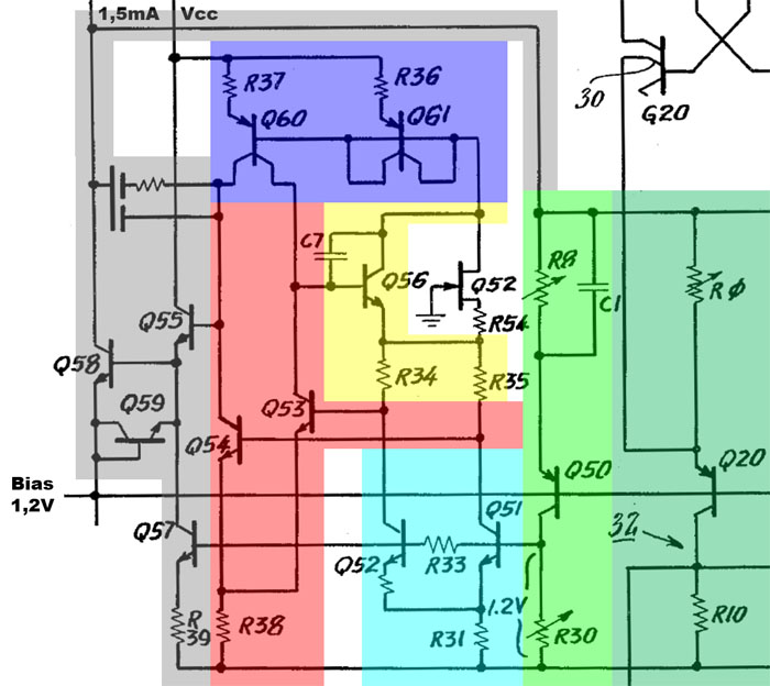
The bandgap reference is based on the well-known principle described in more detail with the AD1403 (https://www.richis-lab.de/REF16.htm). At first sight, however, the circuit is a bit confusing. The core is formed by the transistors Q51/Q52 (cyan). Depending on the currents in the two paths, the transistors Q53/Q54 are driven differently (red). The two transistors are supplied via the current mirror Q60/Q61 (blue), which uses the sum current of the bandgap cell as reference current.

Via the gray path, the potential of the reference current source (light green) is adjusted so that 1,2V is applied to the base of the bandgap reference. If their emitter resistors are set correctly, this voltage is very temperature stable. The following current sources of the DAC (dark green) operate with the potentials of the reference current source.

Capacitance C1 ensures stable operation, as do the capacitors in the gray output stage. Q55 represents a driver, which works with the current sink Q57, which is based on the bandgap reference. In the output stage, transistor Q58 operates with a 1,5mA current source.

The current through the bandgap cell is controlled by Q56 (yellow). The JFET Q52 ensures a clean start-up.


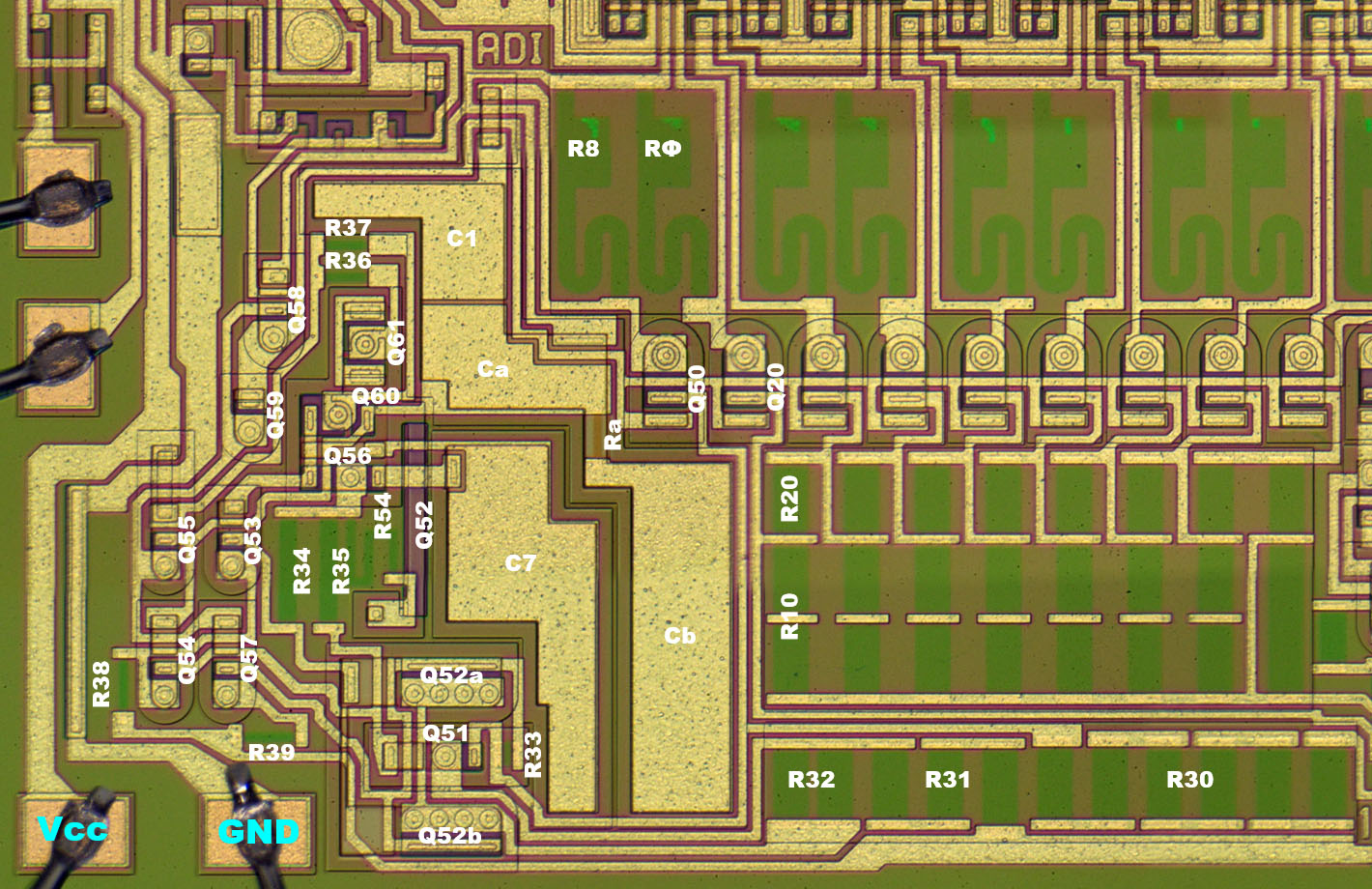
With the reference particularly noticeable are the large capacitors that provide the necessary stability.


The core of the bandgap reference shows the typical structure. On the bottom right, a small transistor is surrounded by a large, two-part transistor. This ensures that both transistors behave as similarly as possible.


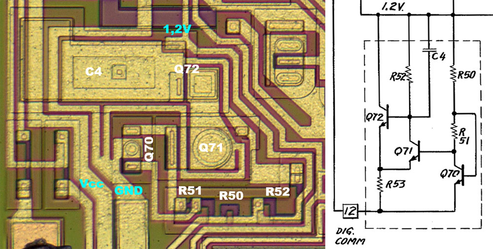
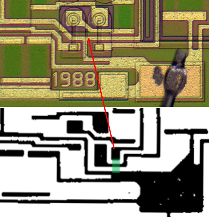
In the shunt regulator for the 1,2V bias, it is noticeable that resistor R53 is missing. R53 is also not visible in the metal layer of the first revision.

The transistor Q72 and the capacitor C4 are integrated into each other.


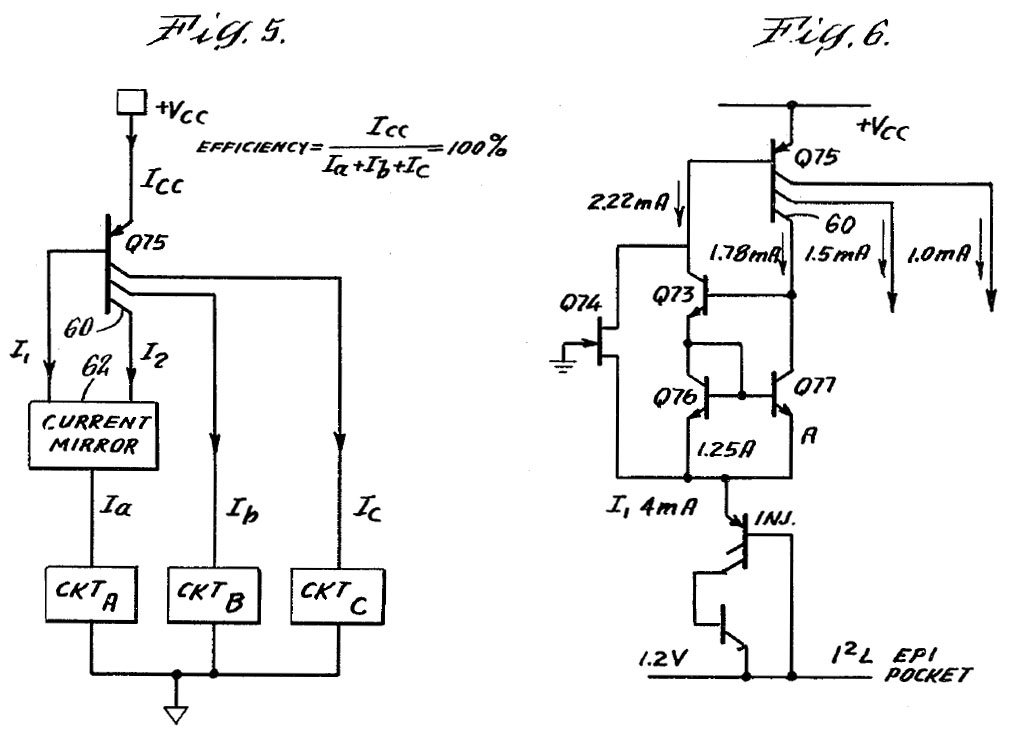
The patent US4323795 emphasizes the efficient generation of the necessary, relatively high working currents. The geometries of the current mirror Q75 and the current mirror Q73Q76/Q77 have been matched so that a constant current is established (Ia). This current can be used directly as a bias current and there is no need for the classic reference path, whose current flow is lost for the actual circuit.

The current source thus supplies the I2L circuit with 4mA, the control output of the bandgap reference with 1,5mA and the control circuit of the I2L buffer with 1mA.


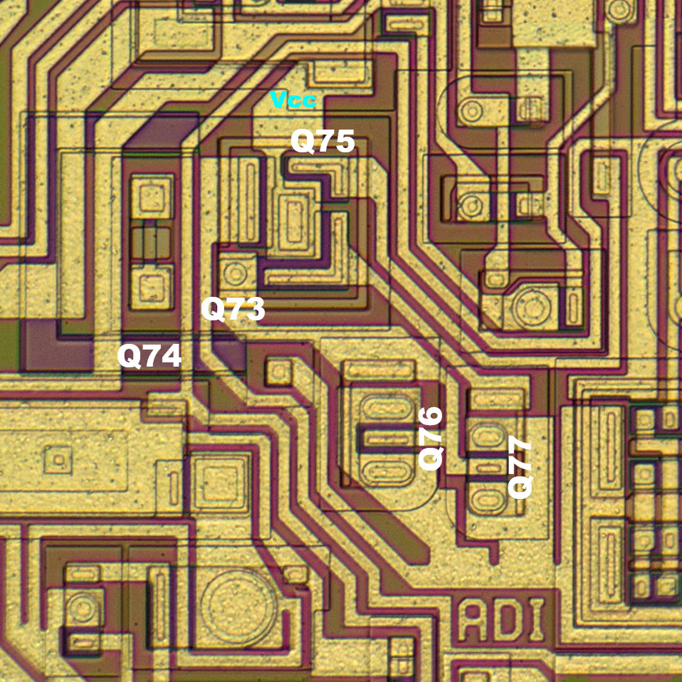
The implementation of the current sources on the die features some interesting structures. Three large collector structures are integrated around the PNP transistor Q75. Due to the close electrical connection, the NPN transistor Q73 is located directly inside these structures. In the lower area, you can see the differently sized transistors Q76/Q77, which supply the I2L area following to the right.


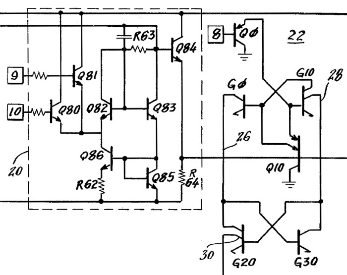
A small circuit links the control signals CS and CE and thus controls the transfer of the applied digital value into the lath.

The transistors with the half emitter arrows are constructed as Integrated Injection Logic (I2L), as described in more detail in the context of the CA3161 (https://www.richis-lab.de/logic22.htm).


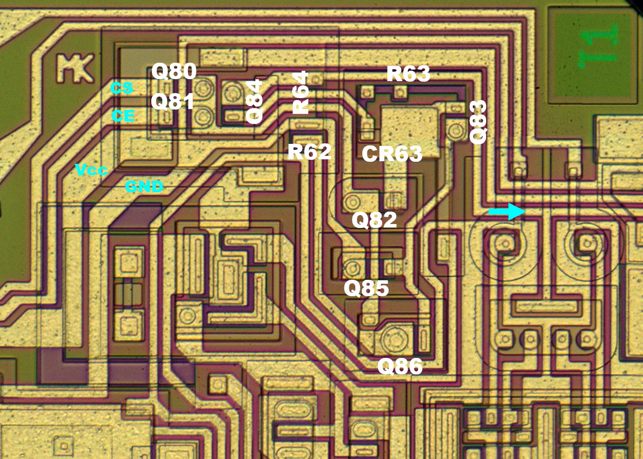
The control circuit of the buffer is integrated in the upper left corner. The resistor R63 has two additional contacts and can thus be adjusted by changing the metal layer. This changes the switching threshold of the inputs.


The use of I2L technology made it possible to integrate the latch in a very space-saving manner. The injection current is fed into the area from the current source on the left and contacts the individual I2L elements with quite low resistance.


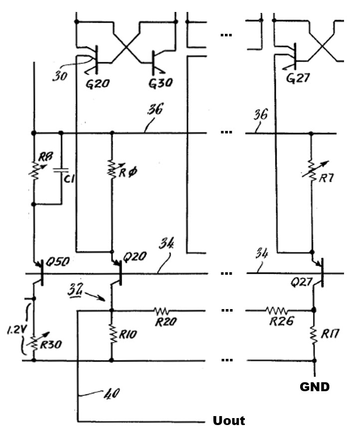
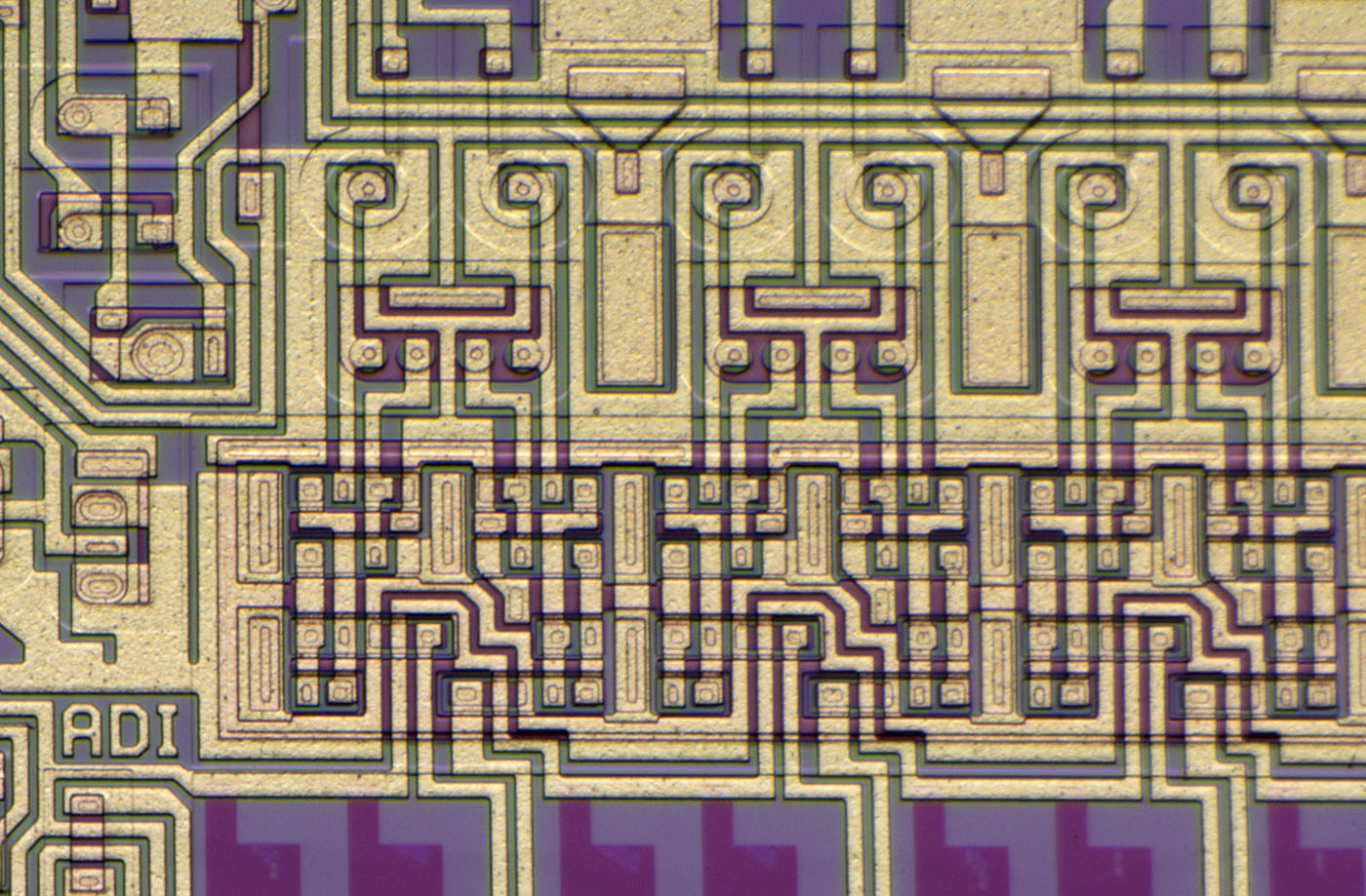
The actual DAC is shown in abbreviated form in the patent circuit. The emitter resistors of the current sources are adjustable to be able to represent a high accuracy. Below the current sources is the R2R divider, which ensures that the current sources further to the right only contribute a portion according to their weighting. The output voltage adjusts between 0V and 400mV.


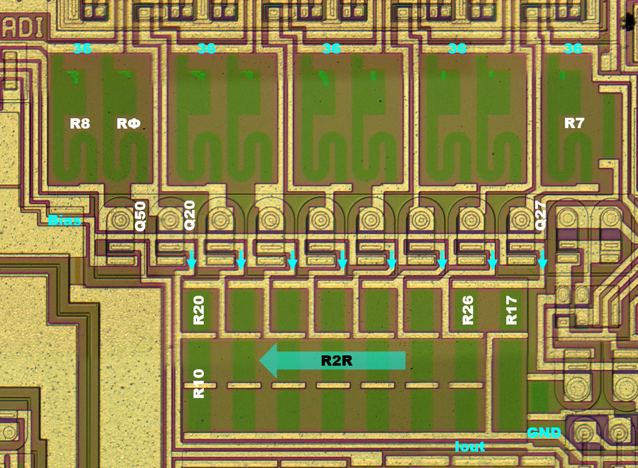
The reference current source (Q50) is integrated directly next to the eight current sources of the DAC and has exactly the same shape. This measure ensures that all current sources behave as identically as possible.

The emitter resistors are clearly visible. Every resistor was tuned. However, the right elements show less alignment traces. The accuracy requirements are lower because of the smaller contribution of the current sources and probably less effort was put into the tuning.

At the top edge, the emitter potential "36" is distributed. In the middle, the PNP transistors generate the necessary currents whose contributions to the output voltage are scaled in the R2R network. To achieve a high symmetry with the resistors, there is a resistor strip under R17, although it is not needed in the circuit.


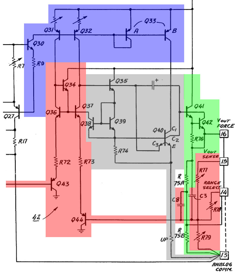
The output amplifier uses the potentials of the DAC current sources to generate its bias currents (blue). The input stage (red) has an unusual design. PNP transistors Q43/Q44 process the output signal of the DAC and the feedback that is fed back from the output. They are located in the emitter paths of current mirror Q34/Q36/Q37.

At the collector of transistor Q37 the signal is passed to the next amplifier stage (gray), which controls the output driver Q41 (green). With R76 Q42 represents an overcurrent protection. Depending on the external connection of the resistors R77/R78/R79, an output voltage range of 0-2,56V or 0V-10V can be set. If the external wiring is missing, the resistors R75A/R75B form a certain negative feedback.

The gray circuit contains a very unusual element with the transistor Q40. The illustration shows a transistor with two emitter terminals and two collector terminals, with one emitter terminal designated C3. The patent US4323795 explains that this particular transistor was integrated to compensate for a fundamental problem that arises when one wants to operate DACs without a negative supply. When the output signal approaches ground potential, the driver stage tends to saturate, which severely degrades the dynamic range of the amplifier.

The additional emitter C3 improves the saturation behavior. In normal operation, no current flows across it. However, if Q40 goes into saturation, the potential at C3 drops below the base potential of Q35. In this state, the additional emitter behaves like a collector and sinks base current from Q35. This results in Q40 being driven less and leaving saturation. The additional collector C2 just provides a Kelvin connection to the collector C1, which reduces the voltage drop in the path of the output stage.


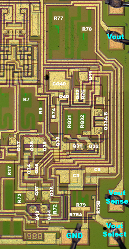
In the output amplifier, the adjusted resistors for the current sources and the voltage divider of the output voltage are clearly visible.


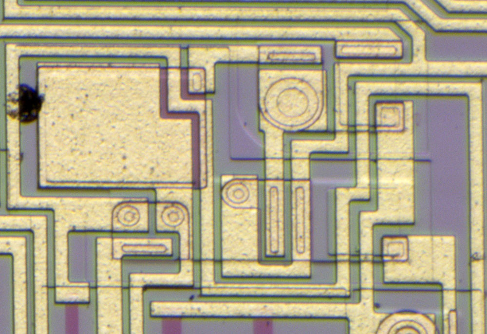
Without the description in the patent it would be difficult to recognize the function of the transistor Q40.


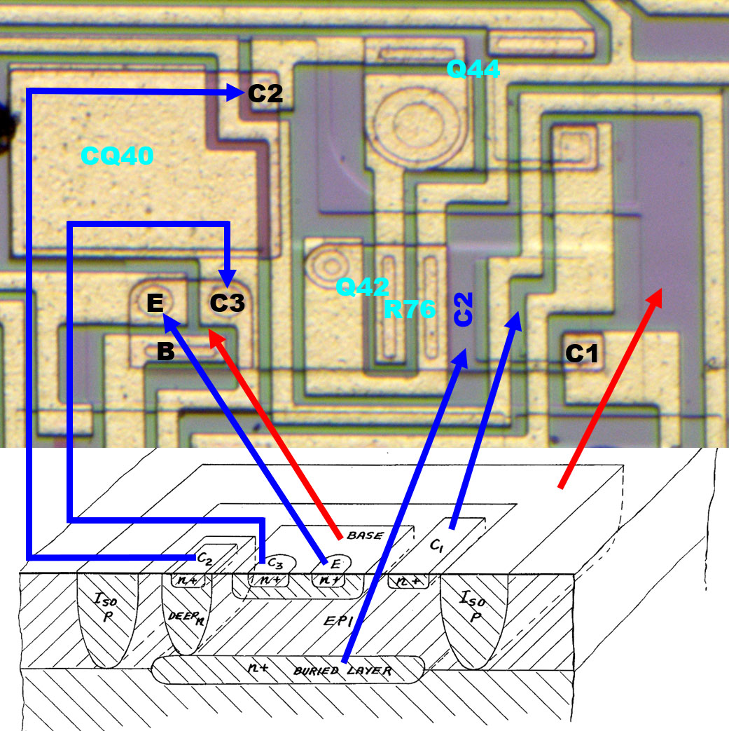
The patent shows a sectional view of this special transistor. C1 and C2 represent a normal collector, with C2 being more low-impedance connected to the active area via a buried, highly doped layer. C3 is a heavily n-doped region within the base area and thus represents an emitter rather than a collector.

In the real structure, the two emitters have the same structure. On the far right, the collector C1 is contacted. The nearly square area then is the surface n+ doping. In the middle of the structure Q42, the current limiting transistor of the output stage, is integrated. Since its collector potential is the C2 potential, it directly uses the collector area of transistor Q40. Shunt R76 has been integrated here too.

The buried collector extends over the whole area of the two transistors and further to the upper left, where it widens and represents the lower electrode of the capacitor CQ40. Finally, the connection from the collector C2 to the output transistor Q44 is located there.


The two PNP input transistors of the output amplifier show an interesting structure. Since the n-doped base is formed via the collector structures of the NPN transistors, a buried collector feed line could be used here in order to be able to represent the undercrossing of a metal line with low impedance. This collector (now base) feed line shows up here as a thin line within the weak n-doped elongated rectangle.


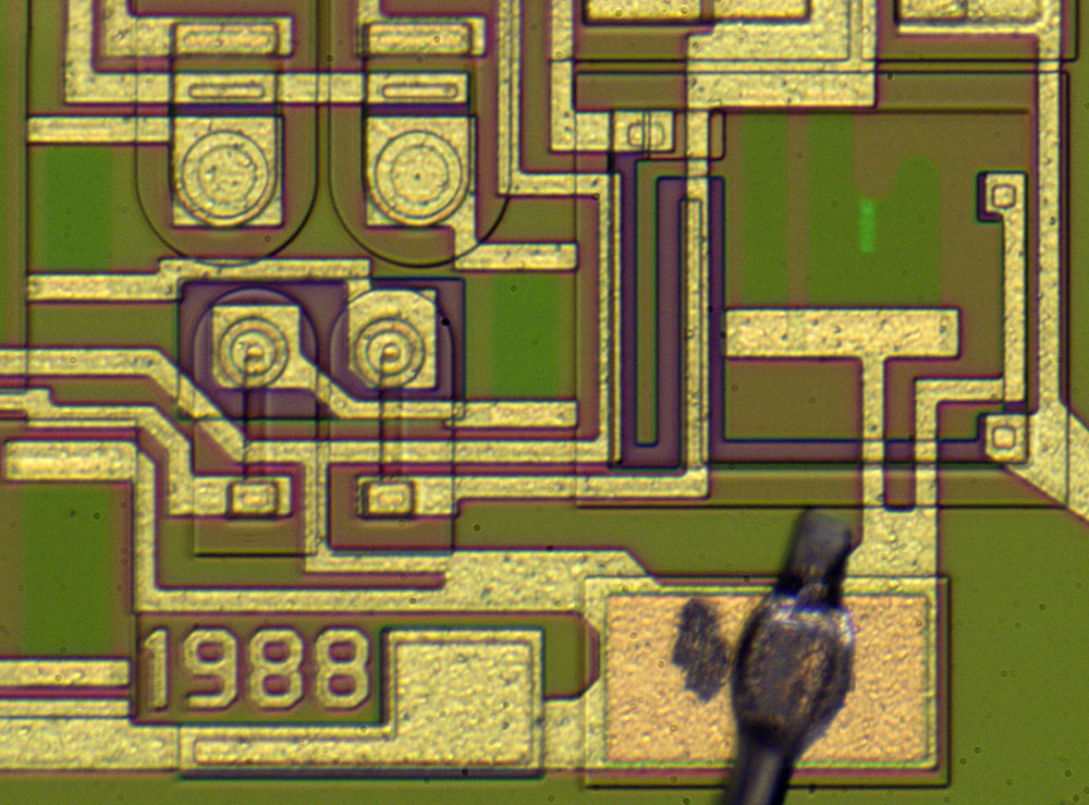
In the schematic in the patent the transistor Q40 is connected to the emitter resistor Rup. On the die this resistor doesn´t exist. The metal layer of the older revision shows that in this version the resistor was probably still present (green).


https://www.richis-lab.de/DAC24.htm

 :-/O
 
The following users thanked this post: D Straney

Offline NoopyTopic starter

  • Super Contributor
  • ***
  • Posts: 1734
  • Country: de
    • Richis-Lab
Re: DACs - die pictures
« Reply #111 on: September 07, 2023, 10:03:36 am »


The HA16633 is a DAC with a resolution of 16Bit developed by Hitachi. Unfortunately, very little information is available about this device.


The HA16330 was used by Hitachi in their DA-1000 CD player. The above advertisement for the DA-1000 is from the magazine Audio, February 1983 (issue 2). It shows the special circuits developed by Hitachi, including the HA16633. However, the DA-1000 was quickly switched to Burr-Brown's PCM53 DAC. The service manual from March 1983 you can find the HA16633, the April 1983 version already refers to the PCM53. The version with the PCM53 was called DA-1000R by Hitachi. It is marked with an R on the back of the case.

The DA-1000 was sold under other names by various other manufacturers: Brandt DAD-001, Continental Edison DAD-9370, Denon DCD-2000, Dual CD 120, JVC XL-V1, Nordmende ADS-2000, Pathe Marconi LA-10, Saba CDP 380, Thomson AD-100.


In the IEEE article "An Untrimmed D/A Converter with 14-Bit Resolution" Hitachi employees describe some details about the operation of the HA16633. The 14-bit DAC presented there was the basis for the HA16633. One was already confident to be able to extend the concept to 16Bit.

As a DAC for a CD player, the HA16330 had to offer a sufficiently high resolution and at the same time be as cheap as possible. In order to be able to do without a time-consuming laser adjustment of the integrated resistors, one integrated a circuit, which makes it possible to determine errors of the DAC. The necessary correction values are stored in a memory and control additional circuits in the area of the DAC during further operation, which correct the error of the output voltage.

The principle of operation is similar to that which would have been planned for the C5360, which is described in the context of the TF536 (https://www.richis-lab.de/DAC09.htm). The errors are determined by comparing the output voltage with a voltage ramp. By this procedure one does not have to determine a voltage exactly, but just a time period, which is a lot easier.


The voltage ramp is generated with an external capacitor. A comparator compares the voltage ramp with the current output voltage of the DAC.

Counter 2 serves the 5 MSBs of the DAC, where the absolute errors of the individual bits have the greatest effect. The counter ensures that all 32 states of these five MSBs are selected in sequence. For each value a correction value is determined.

To develop the correction value, counter 1 counts the pulses of the clock signal that is supplied from outside. If the voltage ramp reaches the potential of the output voltage, the counter stops. The determined value is stored and counter 2 is incremented to adjust the next stage. If the circuit and the clock frequency are designed correctly, then the counter directly generates the necessary correction value, which can easily be stored in the memory.

The "Selector" provides access to the input of the DAC. In normal operation, the five MSBs control not only the DAC, but also the selection of the necessary correction value in memory.


Depending on when the comparator switches, either more or fewer pulses are counted. The number of pulses is proportional to the error of the steps. With a clock signal of 1MHz the 14Bit concept DAC needs 120ms for one run of the ramp.


The voltage ramp of the HA16633 must be sufficiently linear. Critical is the integration capacitor, which must be conncted externally. The most suitable are styrene capacitors whose linearity is sufficient to represent an adjustment of up to 17Bit.


There are two very similar IEEE articles describing the concept of the HA16633. Both documents are titled "An Untrimmed D/A Converter with 14-Bit Resolution". One document was presented at the 1981 IEEE International Solid-State Circuits Conference. The second document can be found in the IEEE Journal of Solid-State Circuits, Vol. SC-16, No. 6. The first document describes just a single alignment. The second document describes a somewhat more complex procedure and also contains a diagram showing the residual errors.

As already shown, the clock signal and the voltage ramp must be adjusted in such a way that the necessary correction value results directly from the state of counter 1. Since it is difficult to reach this operating point exactly, an adjustment takes place within the control logic. If a relevant deviation is detected at the maximum value of the counter during the first adjustment, then the control circuit modifies the number in counter 1 at each stage of the digital-to-analog converter. According to the IEEE article, the adjustment is performed a total of three times.


The service manual of the DA-1000 contains a complete circuit diagram of the CD player, a block diagram of the HA16633 and an adjustment instructions. According to this, in addition to an analog and a digital reference potential, the device is supplied with four other potentials: 12V, 8V, 5V and -5V. In the block diagram pin 31 is marked with the letters INT. In fact, however, it must be called INJ, since the pin supplies the I2L logic of the device ("injector"). The reference voltage is generated internally, output via pin REF OUT and is taken back via pin REF IN. At pin CEX you can apparently connect a capacitor for noise suppression. Most likely, the capacitance de-noises the reference voltage source.

The concept of the error corrector corresponds to a large extent to the concept from the IEEE articles. Pin IVOL can apparently be used to set the slope of the voltage ramp used for adjustment. The integration capacitor is to be connected to the pins INT IN and INT OUT.

Here, too, just the 5 MSBs are corrected. A 6Bit counter activates the individual stages of these 5 Bits one after the other and then disables the clock signal. The second counter that determines the correction values is a 12Bit counter. The RAM takes over the correction values of the 12 Bit counter, but just 8 Bit of it. This fits to the representation in the IEEE articles. But it will be shown that the RAM has just memory cells for 256 Bit and so not more than 8 Bit correction values for the 32 stages can be stored. In normal operation, the RAM is addressed with the five most significant bits that are present at the digital interface. The memory then automatically transfers the appropriate correction values to the DAC.

The function of the so-called "4bit link" remains unclear. There is no explanation in the IEEE articles. The arrow leads to the block "amplifier correction circuit for downstream 11 bits". Its function is equally unclear. The correction circuit for the errors of the DAC is integrated in the DAC block. For this reason, the correction data of the RAM is also routed directly there. Maybe the path "4bit jack" is an error in the block diagram or an inaccurate representation of a function of the control logic. As described earlier there is a correction of the maximum value of the counter.

The pins RO1 to RO8 are not found in the block diagram. In the listing of the connections the interface is described as "connection for RAM test". Apparently one has created an interface to the internal RAM here. This is surprising, since after all there are eight pins that were reserved for this purpose. During production, no detailed measurement of the component was necessary, since no alignment took place. Perhaps this is why the possibility was created to check the initial errors of the DAC and thus the quality of the integrated circuit via this RAM interface after production.


The adjustment instructions of the DA-1000 describe a step that is to be performed on the HA16633. This involves using resistor R403 to adjust the voltage ramp of the DAC to the clock signal. The automatic self-tuning of the HA16633 is apparently triggered every time the door of the CD drive is closed. As a result, a frequency counter at the COUNT pin (TP.6) can be used to count the pulses that control the 12 Bit counter during the adjustment. The target value according to the service manual is 254.000 +/-1.000. A diagram shows that from a deviation of +/-6.000 the distortions increase strongly.

The 254.000 pulses fit the overall picture well. With this number of pulses, the 12 Bit counter can be filled 62 times. The five MSBs of the DAC actively represent 31 stages. This means that the complete calibration is done twice.


[...]

 :-/O
 
The following users thanked this post: oPossum, MegaVolt

Offline NoopyTopic starter

  • Super Contributor
  • ***
  • Posts: 1734
  • Country: de
    • Richis-Lab
Re: DACs - die pictures
« Reply #112 on: September 07, 2023, 10:04:41 am »


If the epoxy is decomposed at high temperatures, the die with dimensions of 5,7mm x 4,8mm can be exposed. A dark layer remains on the surface. This is usually a polyimide layer that protects the circuit and can also be burned and removed at elevated temperatures. Here, however, it is noticeable that lines are surprisingly clearly visible in the dark layer.


The already mentioned IEEE article refers to another IEEE article with the title "Planar Multilevel Interconnection Technology Employing a Polyimide". It describes a special way to apply a second metal layer to an integrated circuit. The unusual feature is that there is a polyimide layer between the metal layers. Another polyimide layer is used as a passivation layer. This technique seems to have been used for the HA16633.


The IEEE article goes on to describe that it is a special polyimide that can withstand even slightly higher temperatures: "polyimide isoindroquinazoline-dione" or PIQ. The temperature resistance is necessary so that the second aluminum layer can be applied to the first polyimide layer.


These more temperature-resistant polymide layers can also be decomposed at elevated temperatures. Unfortunately, the second metal layer is also lost in the process.


This HA16633 was chemically opened at HTV (https://www.htv-gmbh.de/). If this process is mastered, it is even possible to preserve the bondwires, as can be seen here.


The bondwires are completely undamaged chemically and mechanically.


At the edges of the opening the filler contained in the epoxy can be seen. These are very different silicon oxide fragments with a diameter of up to 100µm. For modern components the filler is often specified much more precisely. In some cases even silane is burned to produce silicon oxide with exactly the desired properties.


The chemicals used to dissolve the epoxy have unfortunately dissolved the polyimide too. The second metal layer is partially still present relatively undamaged, but in some cases it has been completely lost. In some places, even the first metal layer has been attacked. As soon as the protective polyimide layer is dissolved, the first metal layer is completely exposed to the acids. In other components that use silicon oxide or silicon nitride as a passivation layer, the metal layer remains protected by the passivation layer apart from the bondpads.


The lines of the second metal layer have set up in some places and partially obstruct the view of the circuit parts below.


[...]

 :-/O
 
The following users thanked this post: Miyuki, D Straney

Offline NoopyTopic starter

  • Super Contributor
  • ***
  • Posts: 1734
  • Country: de
    • Richis-Lab
Re: DACs - die pictures
« Reply #113 on: September 07, 2023, 10:05:45 am »


On the edge of the dies is the designation HA16633.


There are also squares that are most likely used to check the alignment of the masks against each other.


Only one functional test structure is integrated on the die. It is not a simple transistor, but an I2L element. The functionality of an I2L, "Integrated Injection Logic", is described in more detail in the context of the CA3161 (https://www.richis-lab.de/logic22.htm).


Four bipolar transistors are also found in the edge area of the die. However, these structures do not have any contacts.


In the IEEE articles there is a picture of the 14Bit DAC concept. This die is 5,2mm x 4,1mm, contains 1230 I2L gates and 470 so-called linear components.

The individual functional blocks are labeled and in some cases clearly separated from each other. This makes sense, so that the circuit parts do not interfere with each other, but it is also partly due to the different technologies used for control logic, memory cells and the analog peripherals.

Between the functional blocks there is a large number of testpads. The authors of the IEEE articles assume that the silicon area could be reduced by 72% and a package with 28 pins would be sufficient.


The arrangement of the circuit parts is very similar in the HA16633. The signal routing is difficult to analyze due to the damaged metal layer, but you can see some larger bus systems.

The lines of the potentials RO1-RO8 have unfortunately suffered a lot on all pictures. However, they seem to have led to the left to the output of the RAM. This speaks for the theory that the content of the memory could be read with these pins.


The I2L control logic in the right part of the die is located in a light green tub, which clearly distinguishes it from other circuits. Smaller logic areas are also found below the analog section and next to the RAM block.

The control logic consists of several rows where the I2L gates are lined up next to each other. Several thick resistor strips are integrated in the center, representing series resistors in the I2L supply.


The I2L structures can be clearly seen. The mode of operation is described in more detail in the context of the CA3161 (https://www.richis-lab.de/logic22.htm).


The memory area is also clearly visible due to its regular structure. It is surrounded by circuit parts that allow cells to be selected, read out or written.


It is relatively easy to understand that each pair of purple stripes represents a memory cell. However, the functionality is not immediately obvious.


An explanation is provided by the magazine Electronics (February 14, 1972). The six transistors that make up the structures and their interconnection are difficult to see because parts of the silicon are used by several elements. This is at the same time a challenge of this memory technology. One has to adjust the layer thicknesses and dopants in such a way that no uncontrolled conductivity occurs as in a SCR. The individual cells behave like a flip-flop.


In the analog circuit parts in the lower area, the DAC is relatively easy to identify. The other elements like comparator, reference voltage source and integrator are more difficult to identify, mainly because the second metal layer is missing.

Since no adjustment was done during manufacturing, one probably had to accept some weaknesses in the initial accuracy and the temperature drift of the reference voltage. Both parameters are usually calibrated. The IEEE articles specify a temperature drift of 20ppm/°C.


The IEEE articles show how the main DAC is linked to the correction DAC. The 11 MSBs of the DAC (D14-D4) switch 11 equal current sources that are tied to an R2R resistor chain to provide matching contributions to the output level. The 3 LSBs (D3-D1) control 3 transistors connected to a common current sink. The different sizes of the transistors result in suitably stepped current contributions. Above the transistors only simple switches are shown. In fact, they are toggle switches so that the respective current shares do not change. For the same reason, the second 4x transistor is necessary, which is permanently connected to the supply voltage. This is the only way to achieve the necessary ratio of 16:8:4.

The correction DAC offers a resolution of 8 Bit. The 3 MSBs (C6-C4) switch further current sinks and connect them directly to the R2R divider of the main DAC. This saves the integration of another resistor chain. In addition, there is a current sink with five transistors of different sizes above it (C3-C1/4). Here the ratio is 16:8:4:2:1.

The IEEE articles state that the largest errors are generated by the 5 MSBs. Usually the errors are not larger than +/-32LSB (related to 14 Bit). The above design theoretically allows for alignment down to +/-1/4LSB. Practically, the IEEE articles specify +/-1/2LSB, but show results just in the range of +/-1LSB.


The circuit parts of the DACs can be easily identified on the HA16633. In the lower area there are 17 resistors, each of which is represented by a series connection of three slanted resistors (light green). Above them are 14 switchable current sinks and 3 non-switchable current sinks (dark green). Above the current sinks, the R2R current divider is made up of slanted, longer resistor strips (yellow). At the current sinks you can see that bits D8-D6 are connected to correction current sinks (C8-C6).

Above the R2R current divider are the transistors of different sizes, with two current sinks representing the remaining portions of the main DAC (D5-D1) and the correction DAC (C5-C1). The equal size ratios of the main DAC and correction DAC are clearly visible. Above them are the associated toggle switches.

There remains a current sink exclusively connected to a transistor of size "4x" (I_R0). The purpose of this path remains open. The base of transistor I_R0 is connected to the emitters of the transistors C5-C1. An influence in this direction should not take place. It´s not possible to reconstruct to what the collector of the transistor was connected. Maybe a control loop closes here, which sets the operating point of the DAC.


If the IEEE schematic is modified accordingly, it shows that for the extension of the main DAC to 16 Bit, the transistors above the last current sink were just supplemented by two additional, correspondingly smaller transistors. The correction DAC has not changed, whereby now the lowest bits there only reach C1, thus allowing at most a correction by +/-1LSB. With the specifications of the IEEE DAC, one can assume that the HA16633 can adjust to +/-2LSB at most, probably even only to +/-4LSB.


The remaining analog circuit parts are much more difficult to identify.


The circuit of the comparator is shown in the IEEE articles. It should have a response time of 130ns or less.


https://www.richis-lab.de/DAC25.htm

 :-/O
 
The following users thanked this post: ch_scr, D Straney


Share me

Digg  Facebook  SlashDot  Delicious  Technorati  Twitter  Google  Yahoo
Smf