I have updated the optical section of my HowTo:
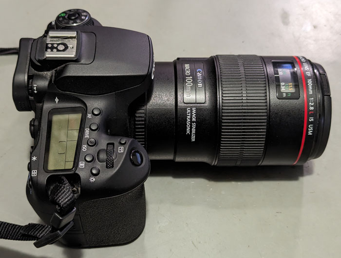
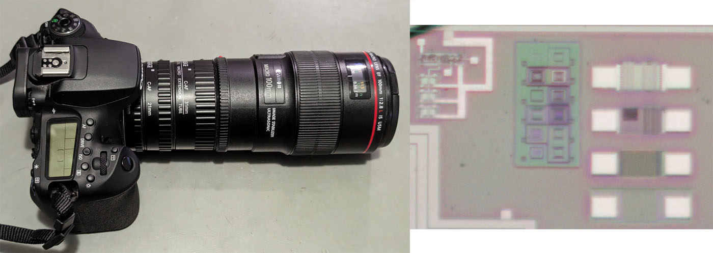
First of all the Canon 90D with the Canon EF 100mm f/2,8L Macro. That´s a surprising performance for a "normal" Macro objective. You can identify the 10µm lines!

The Canon 90D has an APS-C sensor and therefore multiplies by a factor of 1,6. A magnification factor of 1,6 seems very small, but you have to take the high resolution of the digital camera into account. The Canon 90D offers a resolution of 32,5 megapixels. If you are satisfied with 2 megapixels, you already achieve a magnification factor of 26:1. A high pixel density is therefore an advantage here.
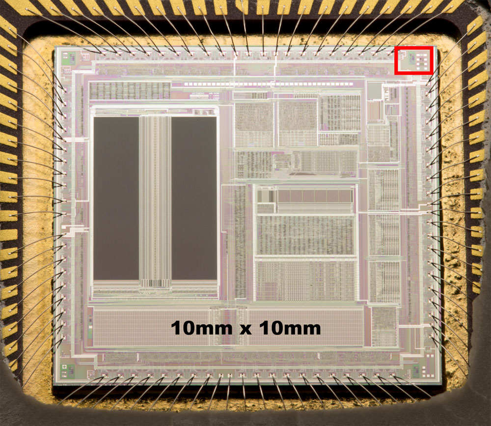
We will take a closer look at this area...
Taking pictures of these small things don´t close the aperture. You need magnification and resolution capacity. Closing the aperture reduces the resolution capacity and your magnification gets useless.
Distance rings can increase the magnification but the pictures is just a little better. With more distance it gets worse.
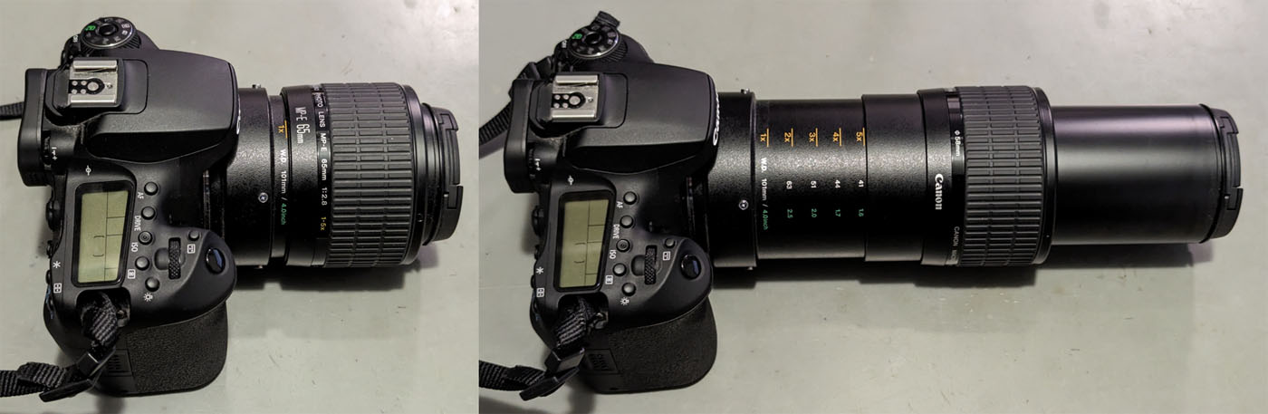
The Canon MP-E 65mm f/2,8 1-5x macro is a magnifying lens that provides image scales between 1:1 and 5:1. On the Canon 90D, this corresponds to an image scale of up to 8:1. If you are satisfied with a 2 megapixel section, this is a magnification factor of 130:1.
One disadvantage of the magnifying lens is the lack of a focus setting. You therefore have to move the camera or the object to focus the image. This is not an easy task with such high magnification factors.
Compared to the Canon EF 100mm f/2,8L Macro, the image quality of the magnifying lens is significantly better.
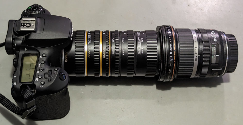
Another option for achieving high magnification factors is the use of so-called retro adapters. This allows the lens to be attached to the camera with the lens normally on the outside. The adapters required for this are available for various camera types and filter threads. The camera can then no longer adjust the aperture and focussing. However, the aperture setting is not usually required and focussing is done manually anyway.
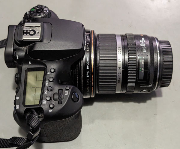
Not every lens is suitable for this application. A small focal length produces a high magnification factor in this configuration. The best results were achieved with the Canon EF-S 10-22mm f/3,5-4,5 shown here. The Canon EF-S 18-135mm f/3,5-5,6 kit lens is also well suited, but this only has a sluggish micromotor focus adjustment, not an ultrasonic motor. The otherwise almost flawless Canon EF 24-70mm f/2,8L produces surprisingly poor images. Looking at the specifications, the Canon EF 28MM f/1,8 USM also seems very suitable. It has a small focal length for a large magnification factor, it has a large aperture, which promises a high resolving power and ultrasonic focussing. In fact, this lens also delivers noticeably poorer results than the Canon EF-S 10-22mm f/3,5-4,5.
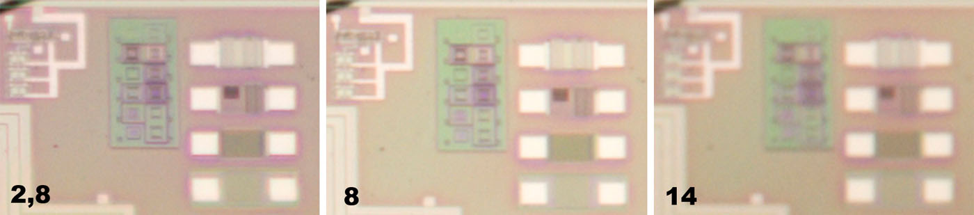
This image shows just how important a small focal length is. The 1:1 image section was taken at the 22mm setting of the Canon EF-S 10-22mm f/3,5-4,5. The limiting factor here is the resolution, but the magnification factor does not offer any major reserves too.
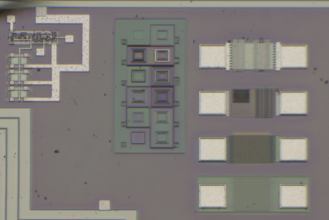
With the 10mm setting, I already had to reduce the image size slightly. At first glance, you might think that the image has deteriorated somewhat, but in fact the opposite is the case. In the top left-hand corner there is a test structure with smaller and larger elements. In the case of the larger elements, you can already see the contacts to the metal layer. Up to this point, however, the magnifying lens still offers better results.
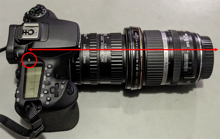
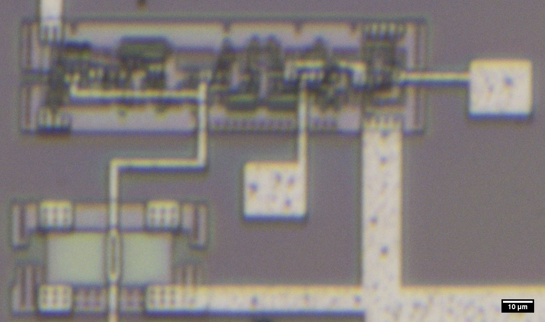
If the retro system is supplemented with distance rings, the magnification factor increases. The images above already show that the resolution is the limiting factor. At the same time, the spacer rings reduce the amount of light reaching the sensor. However, this measure still has a positive effect on the image quality. This can be explained by the fact that lenses are optimised for certain minimum distances. With the Canon EF-S 10-22mm f/3,5-4,5, the close-up limit is 24cm. This is the minimum distance that must be maintained between the object and the camera sensor. Most cameras have a symbol on them that indicates the exact location at which the sensor is located. The distance between the object and the lens is only a few centimetres. With the distance rings, the total length of the optical path is approximately in the range of the close-up limit.
The image quality is significantly better with the 65mm distance rings.
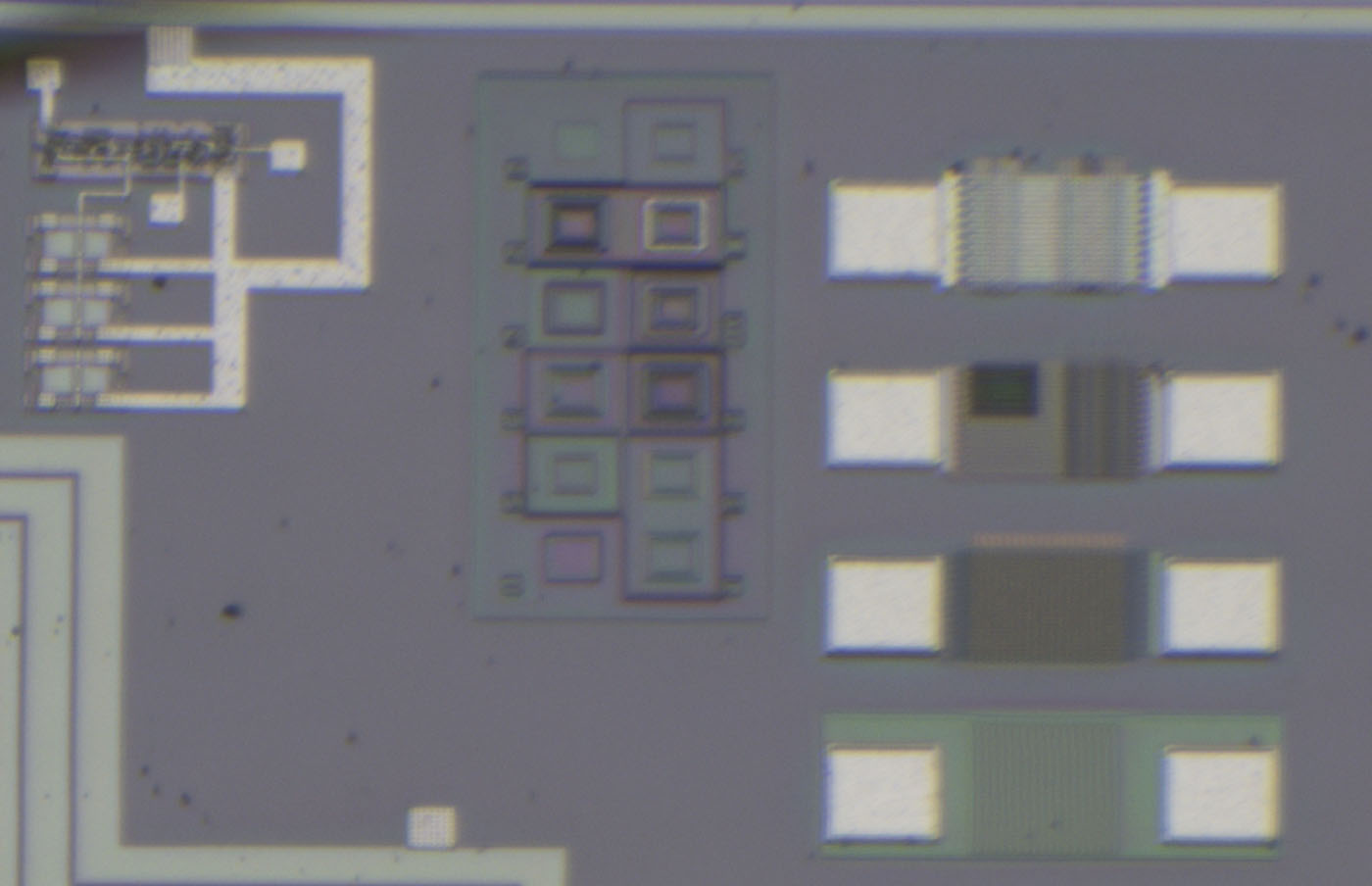
With a second set of spacer rings between camera and lens, the distance increases to 130mm and the image quality improves slightly. The magnification factor increases further.
A third set of spacer rings, which increases the distance to 195mm, does not improve the image quality any further.
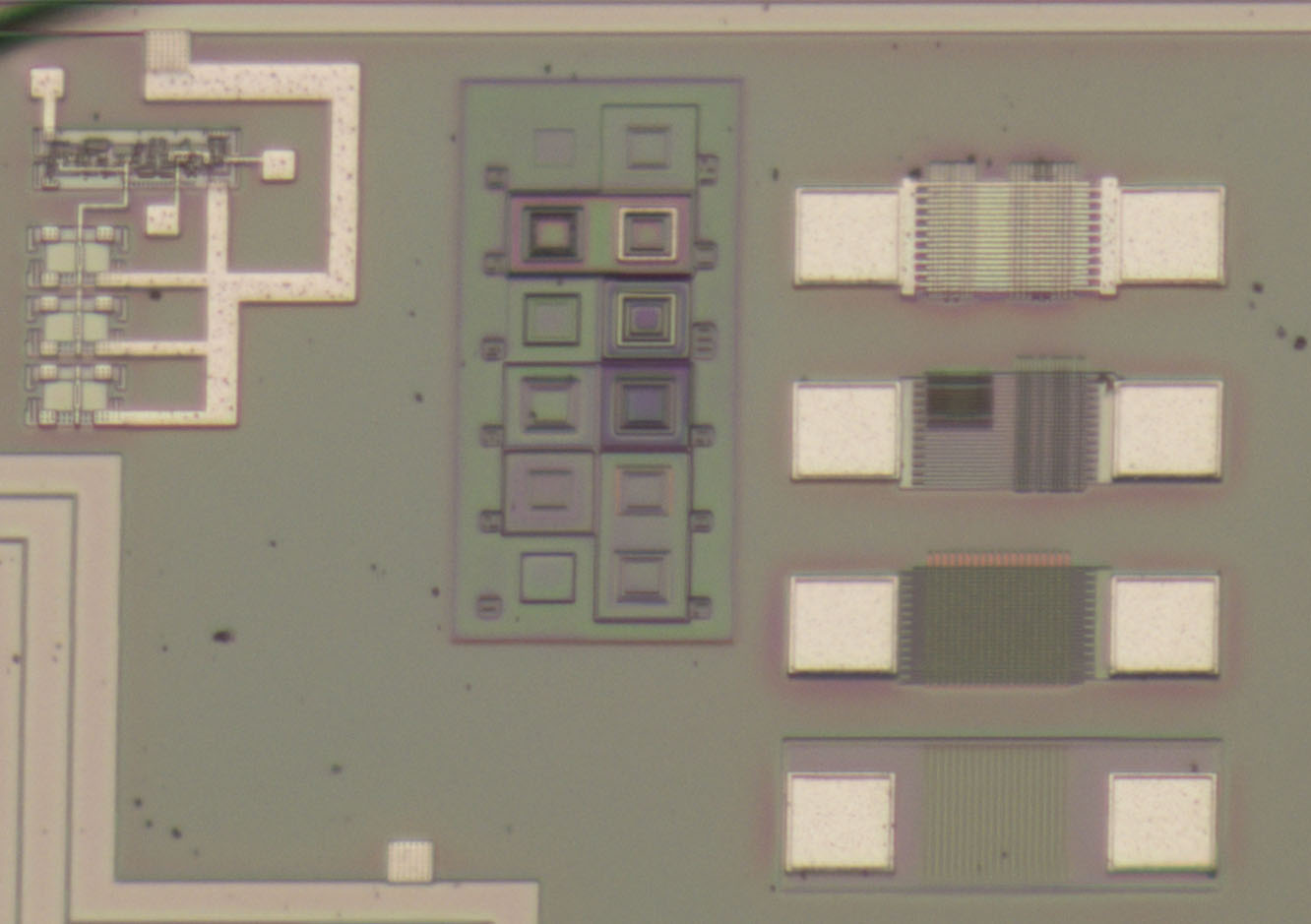
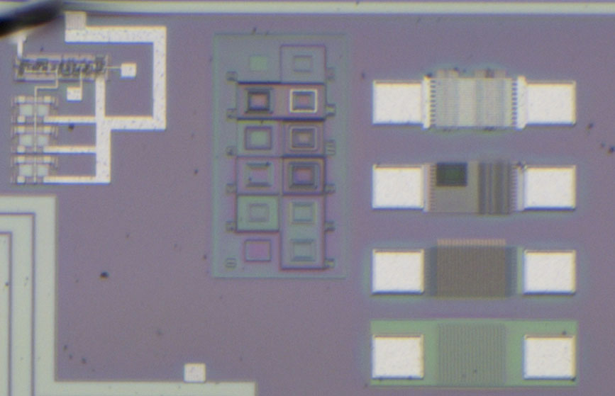
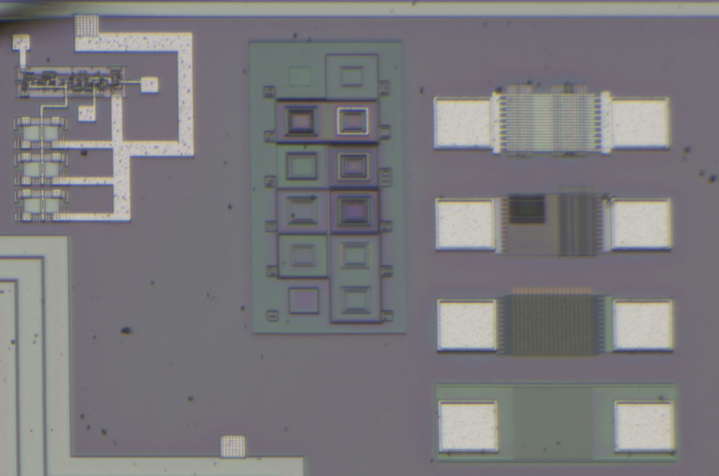
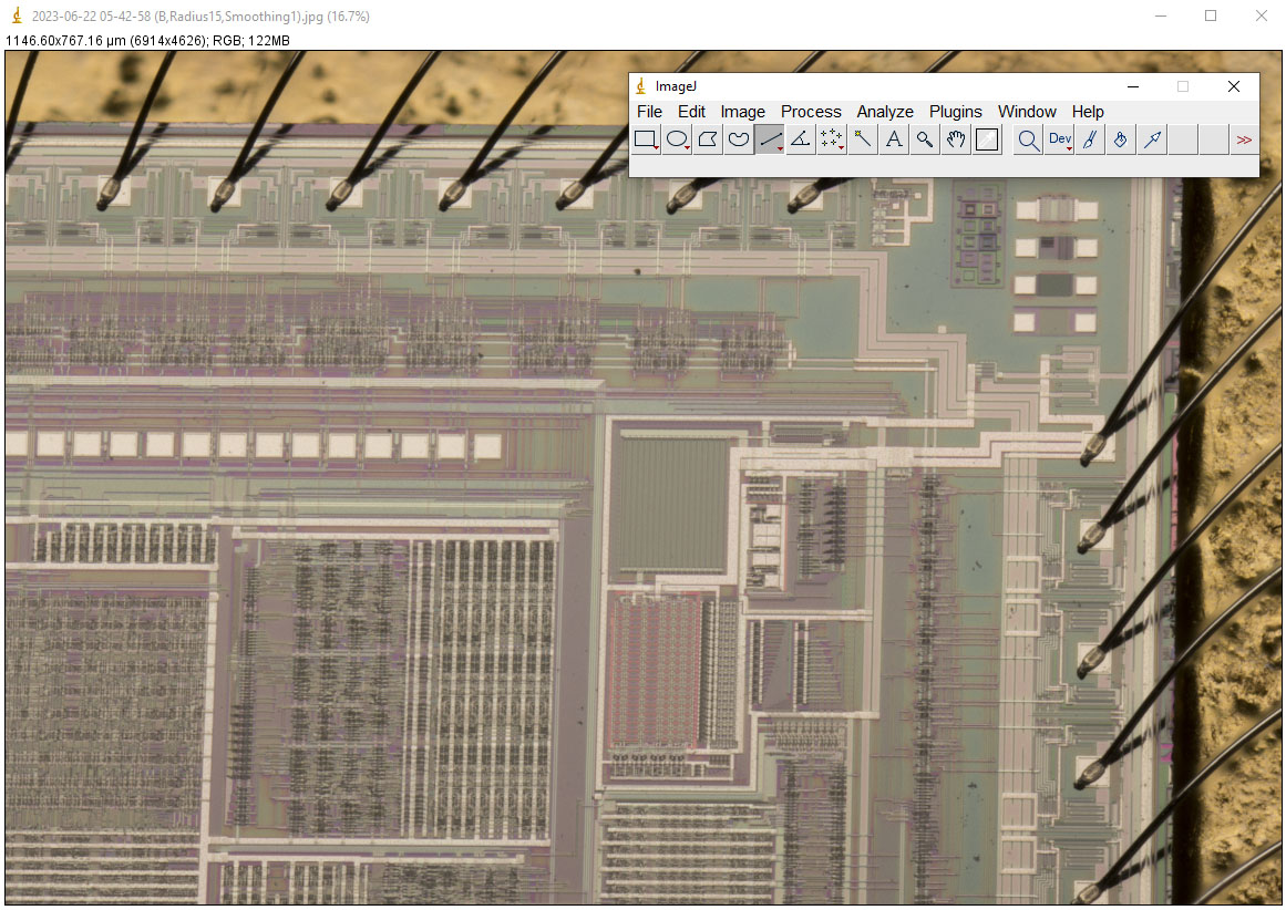
With the Canon EF-S 10-22mm f/3,5-4,5 and 130mm distance rings, one millimetre is imaged with 6.030 pixels. This means that there are six pixels in the distance of one micrometre. The sensor of the Canon 90D is 22,3mm wide and resolves this width with 6.960 pixels. That is 312 pixels per millimetre. This results in a magnification factor of 19,3:1. In relation to a 2 megapixel image section, the factor is 314:1. Here you can see a 1:1 image section. Depending on which structures are involved, elements as small as 1 µm can be recognised.
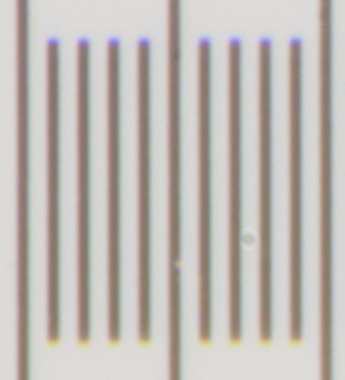
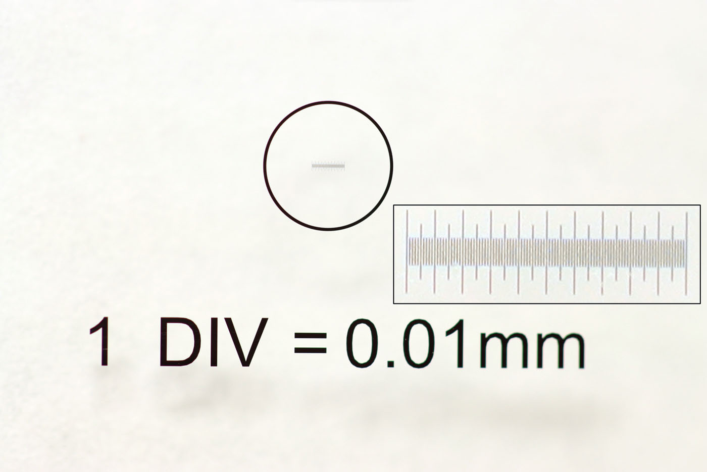
This 1:1 image section shows the lines on the scale with their distance of 10µm.
If you know the magnification factor of the structure, you can carry out measurements in the images. The freeware ImageJ is very well suited for this.
If the image is focussed with the focus ring of the lens, the magnification factor also changes. The focus setting is not saved, resulting in an additional measurement error when calculating the actual size from the number of pixels. In the case of the Canon EF-S 10-22mm f/3.5-4.5, however, the additional measurement error is a reasonable 1%.
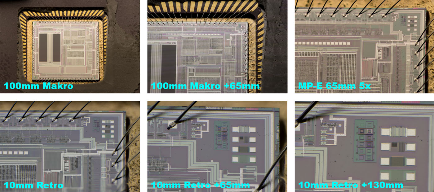
Here you can see the image sections that result from the different configurations. A large magnification factor is desirable in order to make small details visible. At the same time, however, the image section becomes smaller and smaller. You then have to either create panoramic images or take individual detailed images with the appropriate magnification factors.
The high resolution of digital cameras is a great advantage here, as a tolerably large image section remains available even with large magnification factors.
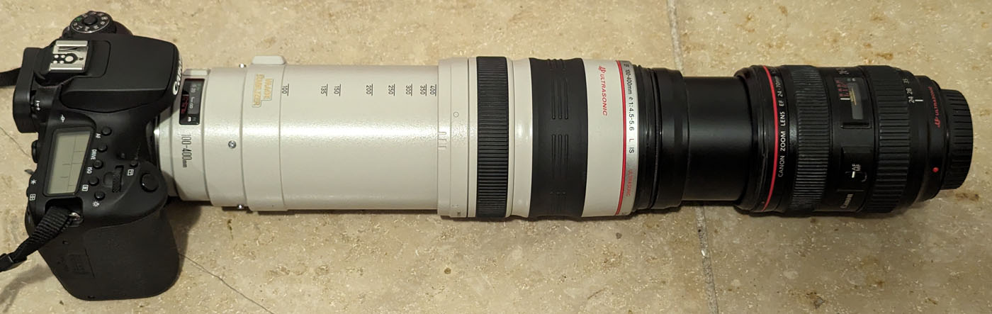

Instead of the spacer rings, you can install a lens in a normal configuration between the camera and the retro lens. This requires an adapter with two matching filter threads. The additional lens adapts the light path of the retro lens to the camera. The magnification factor then corresponds to the ratio of the focal lengths. Here, the Canon EF 100-400mm f/4,5-5,6L IS USM with the Canon EF 24-70mm f/2,8L produces a magnification factor of 16,6:1, in relation to 2 megapixels this would be a magnification factor of 271:1.
Configurations with different lenses were tested. No combination delivers good image quality. The resolution is poorer, especially in the peripheral areas and chromatic aberration is clearly visible.
https://www.richis-lab.de/Howto_Optik.htm 


