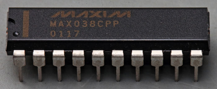
Waveform generator MAX038 (0,1Hz-20MHz)
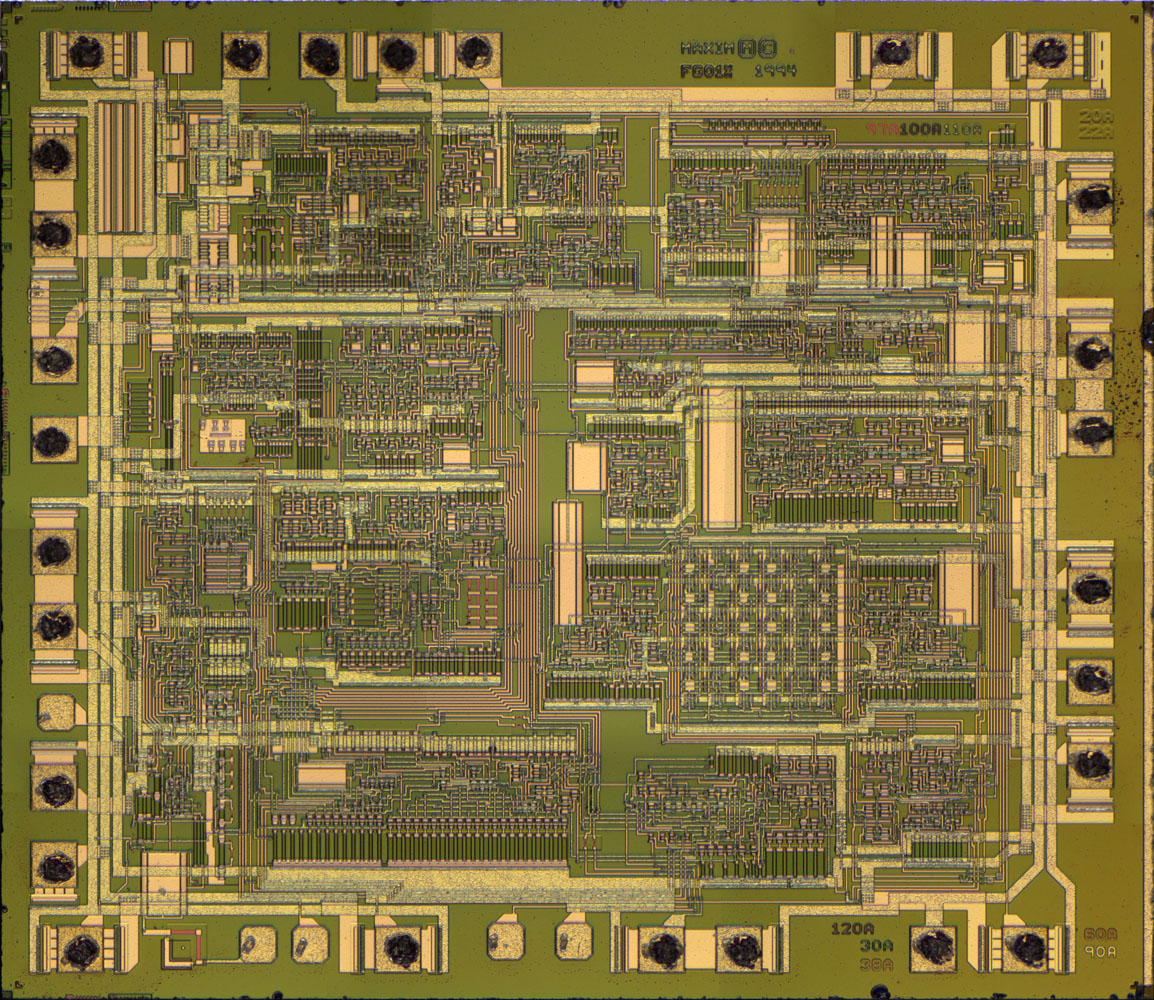
The datasheet states there are 855 transistors. I didn´t count them.

There are a lot of bondpads because important connections were done with two bondwires and there are a lot of independent GND bondpads.
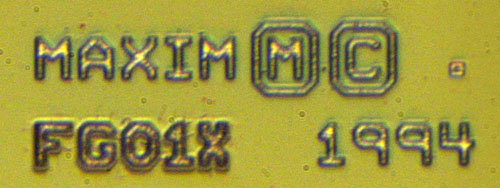
Designed 1994...
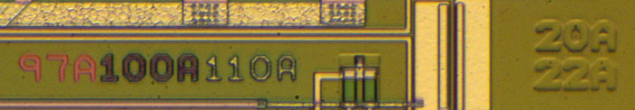
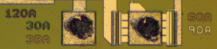
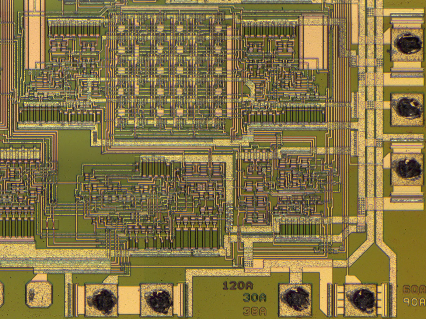
They used the masks 20A, 22A, 30A, 38A, 60A, 90A, 97A, 100A, 110A, 120A
20A and 22A seem to form a buried layers.
The color of 30A is seen in some of the resistors.
It looks like 38A and 60A are just silicon oxide with different thickness. Perhaps 38A is the gate oxide while 60A gives contact from the metal layer to the transistors and resistors.
90A seems to be the first metal layer which would fit with 60A generating vias.
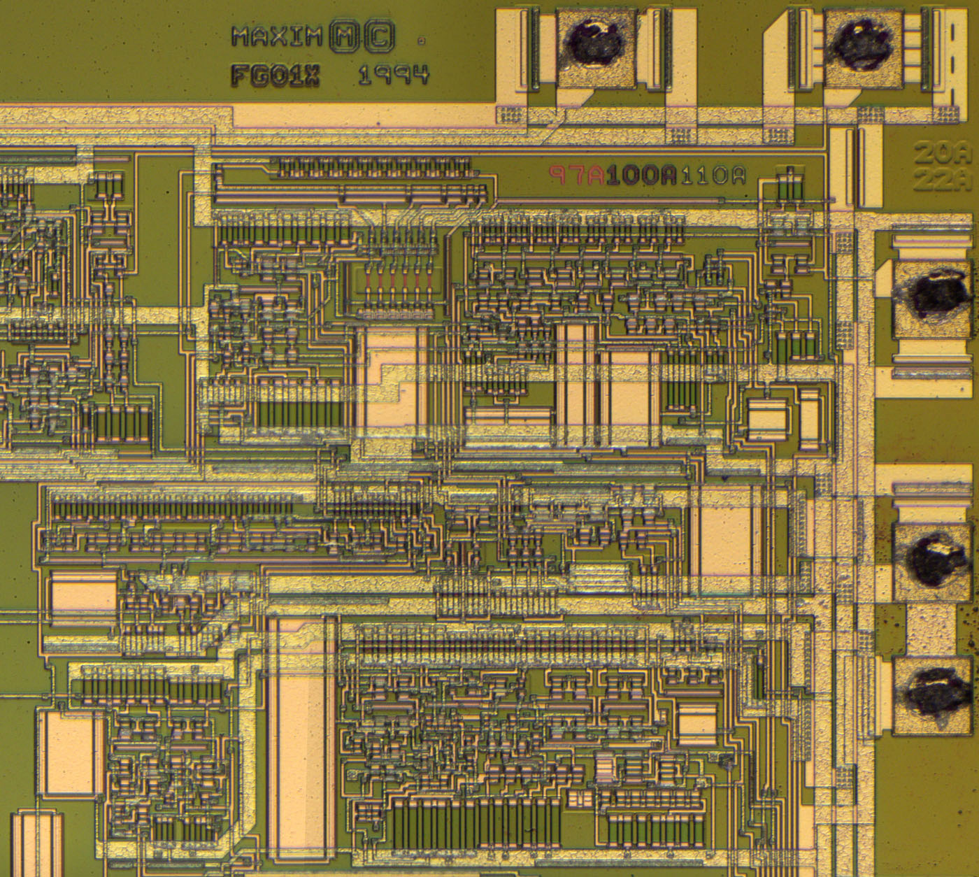
97A adds a red material which can be adjusted with a laser.
110A is the second metal layer.
100A makes contact from the second to the first metal layer.
120A probably forms the bonding areas.
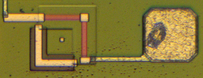
We see such structures quite often whenever there is a laser tuning process.
Cut red wires to adjust the resistors.

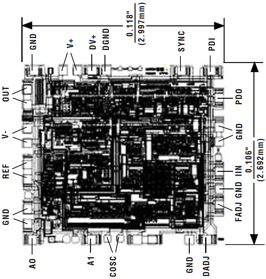
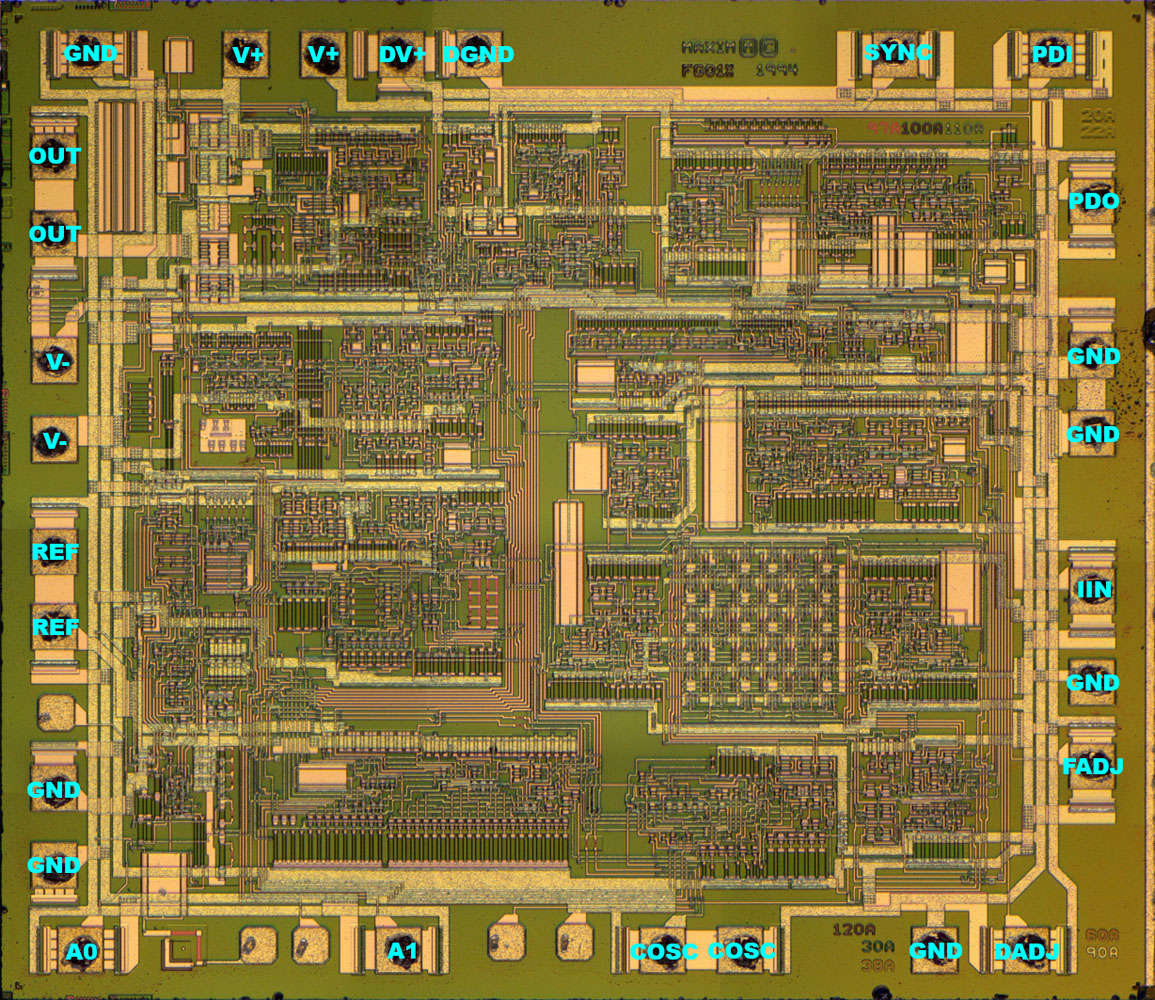
In the datasheet there is a die picture which show the signals of the bondpads.
There is one small mistake in the datasheet. COSC is connected to two testpads.
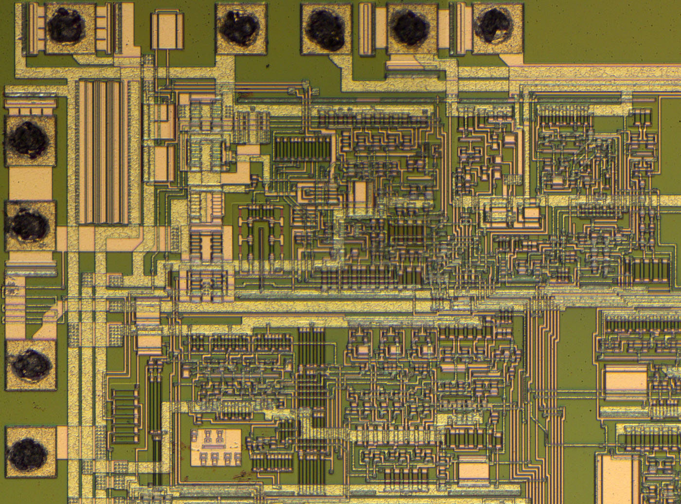
In the upper left corner there are five bigger squares, probably the output driver.
I´m not sure what the purpose of the longer structure in the corner is. It seems it´s just connected to V+ and V-.
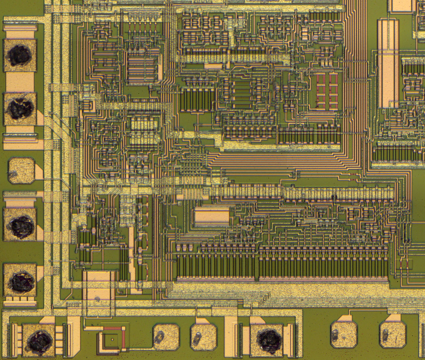
In the right area you can spot two bigger parts. That is the SYNC ouput driver. It is connected to it´s own supply at the upper edge of the die.
The construction of the capacitors is unusual.
The connection of the reference output shows that the voltage reference has to be located in the lower left corner of the die.
There are four testpads probably to adjust voltage and drift. If you track the wires you find four red fuses disconnecting the testpads after adjustment.
REF has its own ground connection. There are a lot of GND connections which are not connected internally.
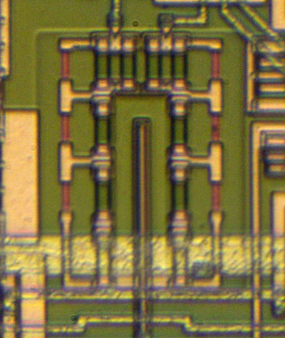
This square structure is interesting. Perhaps that´s the sine shaper. Sine shaper often have repetitive structures.
https://www.richis-lab.de/gen01.htm 


