Author Topic: Different die pictures  (Read 86350 times)

0 Members and 1 Guest are viewing this topic.

Offline NoopyTopic starter

  • Super Contributor
  • ***
  • Posts: 1734
  • Country: de
    • Richis-Lab
Re: Different die pictures
« Reply #125 on: August 04, 2021, 07:59:51 pm »
Wonder how good the charge transfer between capacitors was in the scheme? The CCDs we designed ~50 years ago had CTE better than 0.99999 per transfer and had over 10,000 stages, so the end result was (0.99999)^10,000 for a >90% overall Input to Output Transfer Gain.

Best,

It´s "just HIFI", the CTE won´t be the best in the world.  ::)

Offline NoopyTopic starter

  • Super Contributor
  • ***
  • Posts: 1734
  • Country: de
    • Richis-Lab
Re: Different die pictures
« Reply #126 on: August 07, 2021, 03:37:58 am »


Here we have the next part of the GDR telephone system (https://www.richis-lab.de/phone.htm), the U1021, the so called "Zeitlagensteuerung".


Well just some logic...


...and two nice little (digital) phones.


...and some dirt.  :-/O


https://www.richis-lab.de/phone08.htm

 :-/O
 
The following users thanked this post: RoGeorge

Offline NoopyTopic starter

  • Super Contributor
  • ***
  • Posts: 1734
  • Country: de
    • Richis-Lab
Re: Different die pictures
« Reply #127 on: August 11, 2021, 08:41:34 pm »
We had the SDH105 and the SDH112:
https://www.richis-lab.de/loco01.htm
https://www.richis-lab.de/loco03.htm


Now the last one, the SDH119 in a QFN24 package.


The die is 2,5mm x 2,3mm.


No locomotive, no D&H, just RR...


Logic array with big supply lines left and right.


There are 12 transistor arrays. Two outputs use 4 of these each giving us 0,3A max current. The other two outputs use 2 of these each giving us 0,15A max current.
The area on the left probably is the driver and protection circuit.


H-bridge driver and motor EMF feedback.


Supply area
There is a 5V regulator to supply a PIC and a undervoltage signal.


https://www.richis-lab.de/loco03.htm

 
The following users thanked this post: RoGeorge

Offline Ranayna

  • Frequent Contributor
  • **
  • Posts: 865
  • Country: de
Re: Different die pictures
« Reply #128 on: August 12, 2021, 03:02:10 pm »
The phone ICs are absolutely fascinating.
I am administering various IP based phone systems, with barely a contact to non VoIP.
Much of is is now running virtualized on bog standard x86 servers.

It is amazing how much specialized hardware existed before VoIP took hold.
 

Offline NoopyTopic starter

  • Super Contributor
  • ***
  • Posts: 1734
  • Country: de
    • Richis-Lab
Re: Different die pictures
« Reply #129 on: August 12, 2021, 03:13:27 pm »
I totally agree with you.  :-+
Today it looks like you just need a simple ADC a simple DAC and the rest is done by a microcontroller.  ;D

Offline NoopyTopic starter

  • Super Contributor
  • ***
  • Posts: 1734
  • Country: de
    • Richis-Lab
Re: Different die pictures
« Reply #130 on: August 15, 2021, 04:04:14 am »
I have created an alphabetical overview containing all the parts I have documented:

https://www.richis-lab.de/semiconductors.htm

Quite a long list...  :o 8)
 
The following users thanked this post: SeanB

Offline Koray

  • Regular Contributor
  • *
  • Posts: 87
  • Country: tr
Re: Different die pictures
« Reply #131 on: August 16, 2021, 08:40:01 am »
Hi Richi, your website and all these work you have done is amazing. I can spend hours there, learning many new things. Thank you for your effort!
K.
 

Offline NoopyTopic starter

  • Super Contributor
  • ***
  • Posts: 1734
  • Country: de
    • Richis-Lab
Re: Different die pictures
« Reply #132 on: August 16, 2021, 08:46:25 am »
Thanks a lot!
It´s always good to hear there are people interested in my work.  :-+

Offline NoopyTopic starter

  • Super Contributor
  • ***
  • Posts: 1734
  • Country: de
    • Richis-Lab
Re: Different die pictures
« Reply #133 on: August 17, 2021, 07:08:11 pm »
We had a look into the Coolaudio V3205 / Shanghai Belling BL3205. Now let´s take a look into an old BBD built by Matsushita (Panasonic)!


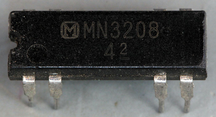
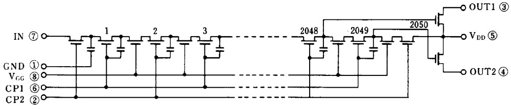
The MN3208 is a NMOS BBD with 2048 stages.


Interesting: The schematic in the datasheet looks very similar to the schematic in the datasheet of the Coolaudio V3205 / Shanghai Belling BL3205! Of course there are less stages but the symbols the letters and everything looks quite similar.
Coolaudio bought a lot of knowledge, patents and people for their vintage portfolio. It looks like they went shopping at Matsushita.


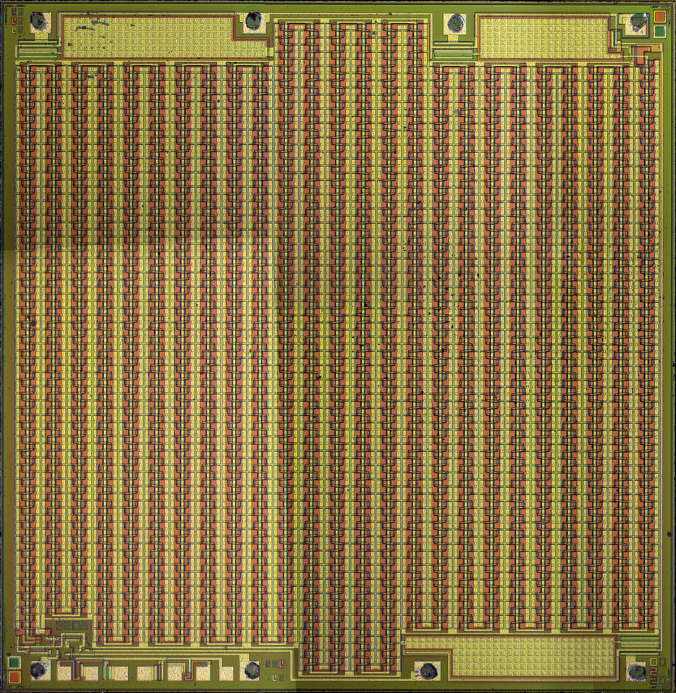
The die is 3,0mm x 3,0mm. The global structure is similar to the Coolaudio V3205 / Shanghai Belling BL3205 but it´s not exactly the same.


3208  :-+
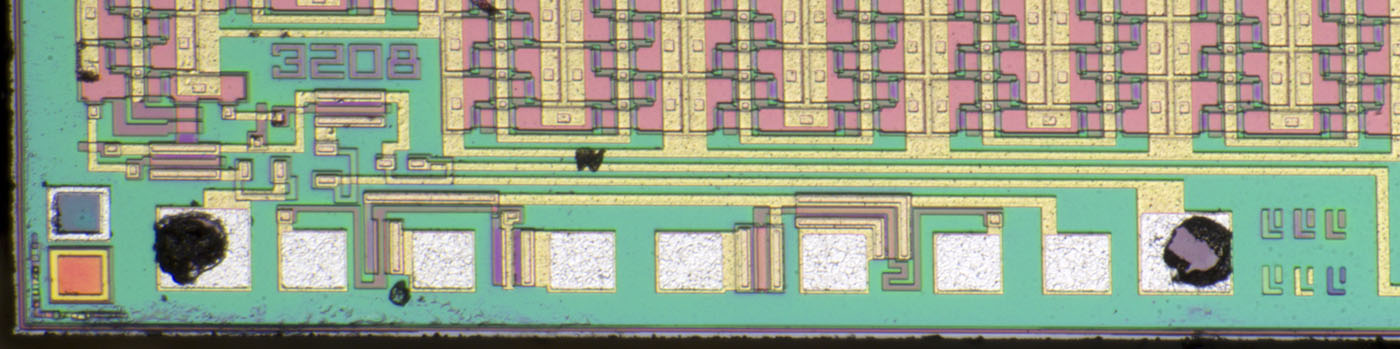
...and some test structures.


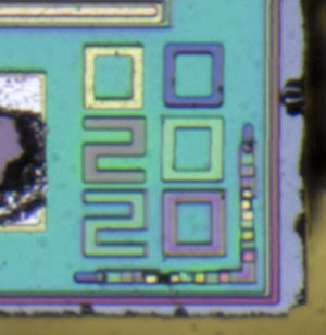
In the corners there are right angled lines that clearly show if there is a misaligned mask.
It looks like they used six masks and two of them were modified two times.


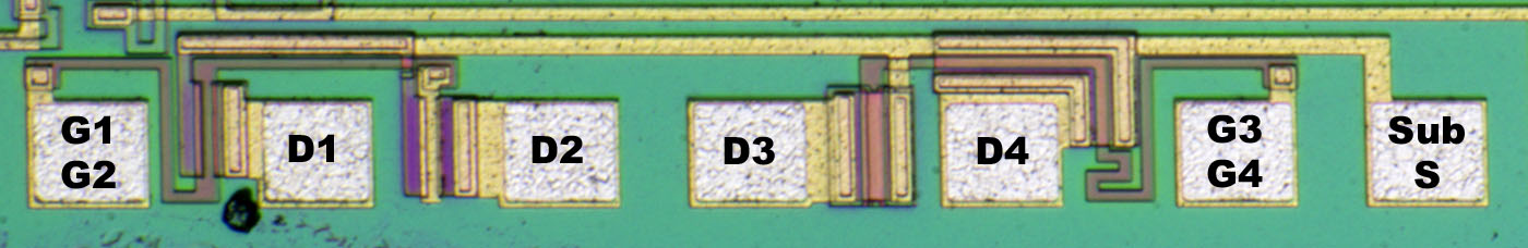
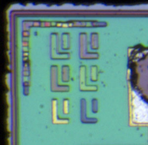
The test structure contains four transistors. All transistors share the same source potential that is connected to the substrate too. T1 and T2 share their gate potential and T3 and T4 share their gate potential.
T1 and T2 use the substrate in their active area. While T1 is equipped with a polysilicon gate T2 switches with a metal gate. In my view that is NMOS.
It looks like T3 and T4 are integrated on a purpel area. Probably that is PMOS. In the gate area of T3 there is kind of a notch. :-//


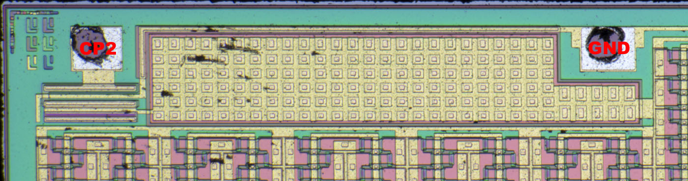
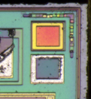
The clocks CP1 and CP2 and the bias Vgg have the same big structures at their inputs as in the Coolaudio V3205 / Shanghai Belling BL3205. Probably protection against negative voltages.


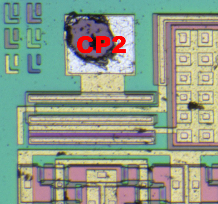
But if we take a closer look we find an additional ESD protection. Under the bondpad there is a C-shaped resistor. Under the resistor there is a metal structure which acts as a gate. Since the metal gate has a thicker oxide than the polysilicon gate the transistor is normally off. But with high voltages (ESD) the transistor is switched on and drains charge to the substrate.


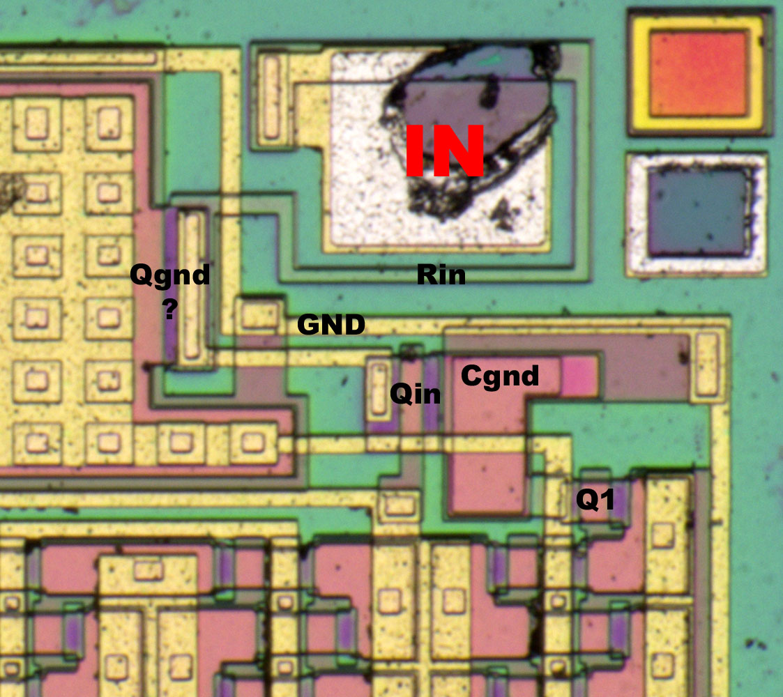
We know the input structure but here we have an additional part. Qgnd? is not mentioned in the datasheet. It looks like the end of the input resistor is placed near the GND plane of the big undervoltage protection structure of Vgg. The lower plane of the protection structure (which is connected to Vgg) is extended to this area what probably produces a MOSFET. I assume that gives us a pull down resistor at the input.
Cgnd looks like it easily could be modified to get more or less input capacitance.


The BBD structure is similar to the Coolaudio V3205 / Shanghai Belling BL3205. The proportions are a little different but not very much.


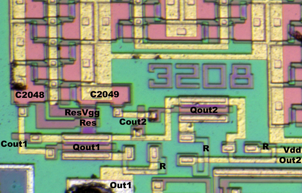
Here we have the two output driver connected to the stages 2048 and 2049.
I wasn´t perfectly clear at the Coolaudio V3205 / Shanghai Belling BL3205 (perhaps a little wrong  ::)): You need these two outputs and you have to connect them because every second stage is empty due to the working principle of a BBD.
In the MN3208 the Res stage that disposes the charges to Vdd is clearly visible. It´s a cascode switch as every other switch in the BBD.
In the driver lines of the output transistors there are very small capacitors connected to Vdd which we haven´t seen in the Coolaudio V3205 / Shanghai Belling BL3205. I assume these capacitors reduces the risk of oscillations.


Some more pictures:
https://www.richis-lab.de/bbd02.htm

 :-/O
 
The following users thanked this post: SeanB, xrunner, RoGeorge

Offline NoopyTopic starter

  • Super Contributor
  • ***
  • Posts: 1734
  • Country: de
    • Richis-Lab
Re: Different die pictures
« Reply #134 on: August 27, 2021, 03:36:20 am »


Here we have the next part of the GDR telephone system (https://www.richis-lab.de/phone.htm), the U3210, the so called "PCM-Empfangsschaltung". No datasheet, no more information.  :(


That´s an interesting test structure...


Input and output...


That area probably contains memory.


https://www.richis-lab.de/phone09.htm

 :-/O
 
The following users thanked this post: SeanB

Offline NoopyTopic starter

  • Super Contributor
  • ***
  • Posts: 1734
  • Country: de
    • Richis-Lab
Re: Different die pictures
« Reply #135 on: August 27, 2021, 08:38:51 am »


That´s an interesting test structure...

Aha! That´s a ring counter, an easy way to check the process quality! The faster the better.  :-+

Offline NoopyTopic starter

  • Super Contributor
  • ***
  • Posts: 1734
  • Country: de
    • Richis-Lab
Re: Different die pictures
« Reply #136 on: August 27, 2021, 03:01:23 pm »


Does anyone know this logo?  :-//
« Last Edit: August 27, 2021, 06:04:50 pm by Noopy »
 

Offline NoopyTopic starter

  • Super Contributor
  • ***
  • Posts: 1734
  • Country: de
    • Richis-Lab
Re: Different die pictures
« Reply #137 on: August 27, 2021, 03:17:20 pm »


And one more question. Does anyone know what that is?
The structures on the die look like a switched capacitor DAC or ADC. But I´m not sure about that.
On the die there are the numbers M7082D.

 :-//
« Last Edit: August 27, 2021, 06:01:28 pm by Noopy »
 

Offline bsdphk

  • Regular Contributor
  • *
  • Posts: 198
  • Country: dk
Re: Different die pictures
« Reply #138 on: August 27, 2021, 05:56:57 pm »
"WE" is very probably Western Electric, so likely telefone related.

 
The following users thanked this post: Noopy

Offline NoopyTopic starter

  • Super Contributor
  • ***
  • Posts: 1734
  • Country: de
    • Richis-Lab
Re: Different die pictures
« Reply #139 on: August 27, 2021, 06:03:10 pm »
"WE" is very probably Western Electric, so likely telefone related.

Sounds plausible!  :-+

Switched capacitor DAC/ADC and a telephone system would match quite well.

Anyone some more information?

Offline NoopyTopic starter

  • Super Contributor
  • ***
  • Posts: 1734
  • Country: de
    • Richis-Lab
Re: Different die pictures
« Reply #140 on: August 31, 2021, 03:48:47 am »


We had a look into the Coolaudio V3205 built with a Shanghai Belling BL3205 (https://www.richis-lab.de/bbd01.htm).
Here we have a genuine V3205.


The die is 4,3mm x 3,7mm.


I don´t know what logo that is and I don´t know what WXMI 2 stands for.


I don´t know...


There are quite a lot teststructures in the cutting area.


The input is the same as in the other BBDs we have seen.
The protection circuits are the same too.


BBD structure, nothing special...


Business as usual


The output circuit is the same as in the BL3205 (https://www.richis-lab.de/bbd01.htm). There is no additional gate capacitor at the output transistors as we have found them in the MN3208 (https://www.richis-lab.de/bbd02.htm).


https://www.richis-lab.de/bbd03.htm

 :-/O
 
The following users thanked this post: RoGeorge

Offline NoopyTopic starter

  • Super Contributor
  • ***
  • Posts: 1734
  • Country: de
    • Richis-Lab
Re: Different die pictures
« Reply #141 on: September 02, 2021, 03:18:25 am »


Here we have the next part of the GDR telephone system (https://www.richis-lab.de/phone.htm), the U3220, the so called "PCM-Sendeschaltung". No datasheet, no more information.  :(

A lot of special digital stuff...


https://www.richis-lab.de/phone10.htm

 :-/O

Offline NoopyTopic starter

  • Super Contributor
  • ***
  • Posts: 1734
  • Country: de
    • Richis-Lab
Re: Different die pictures
« Reply #142 on: September 03, 2021, 03:53:20 am »


TiN gave me a Fluke 842591, a RMS converter used for example in the Fluke 5790A and the Fluke 792A.


The application note of the Fluke 792A shows what is inside the Fluke 842591. The input signal heats the left resistor. Unlike the LT1088 (https://www.richis-lab.de/LT1088.htm) the heater temperatures are monitored with two complete transistors. You build a differential amplifier with these transistors and a opamp does the heating of the second resistor so you get exactly the voltage that gives you the same amount of heat as the input signal, the RMS voltage.


The sensor is shielded on the back side.


The converter is quite small compared to the package.


The die was damaged in the upper right corner. It is placed on a small additional ceramic plate. Perhaps it´s for mechanical isolation or for better handling in the production.


The die is just 0,06mm thick to get a low thermal mass.


There are two islands with a edge length of 0,36mm each containing a resistor and a transistor. The islands are fixed just by the metal layer the rest of  the silicon is etched away.
Everything is quite symmetrical. The left element is damaged due to overheating.


Nine masks? Number 6 was remastered eleven times?  :o


The heater resistors are tuned. In the lower part we see the base area of the transistors. The whole island is the collector material. The inner side contact is the emitter. The middle contact is the base. It´s interesting that both contacts show two circles. At the emitter one of the circles is the emitter area the second is the via but why is there a second circle at the base contact? You can contact the p area directly. Perhaps it´s something special. The application note tells us it´s a special low noise transistor.
The overheating damaged the heater metal contact and the transistor metal contact. Due to the thermal isolation I assume you don´t need much power to overheat the structures.


Here you see the island flying.  ;D


The metal layer of the damaged side tried to leave the island.  ;D


A few more pictures here:

https://www.richis-lab.de/RMS01.htm

 :-/O

Offline TiN

  • Super Contributor
  • ***
  • Posts: 4543
  • Country: ua
    • xDevs.com
Re: Different die pictures
« Reply #143 on: September 03, 2021, 04:06:46 am »
Magical photos, thank you very much for all the efforts.  :-+
These sensors are also used in all 5700/5720/5730 and 5725 Flukes.  ;)
YouTube | Metrology IRC Chat room | Let's share T&M documentation? Upload! No upload limits for firmwares, photos, files.
 

Offline NoopyTopic starter

  • Super Contributor
  • ***
  • Posts: 1734
  • Country: de
    • Richis-Lab
Re: Different die pictures
« Reply #144 on: September 03, 2021, 04:07:43 am »
Thanks for the part!
It was a pleasure!  8)

Online mawyatt

  • Super Contributor
  • ***
  • Posts: 3267
  • Country: us
Re: Different die pictures
« Reply #145 on: September 03, 2021, 10:47:40 am »
Nice images :-+

Recall the earlier versions (before 85) of this Fluke RMS technique used a thinned die suspended by the wire bonds. The backside selective chemical etch similar to what BAW devices used is a better mechanical solution for low thermal mass and isolation, and of course shock and vibration sensitivity.

Best,
Curiosity killed the cat, also depleted my wallet!
~Wyatt Labs by Mike~
 

Offline NoopyTopic starter

  • Super Contributor
  • ***
  • Posts: 1734
  • Country: de
    • Richis-Lab
Re: Different die pictures
« Reply #146 on: September 03, 2021, 11:40:01 am »
Thanks!  8)

Perhaps sometime I get the older version too. I'm sure that would give us some more nice pictures.  :-+

Offline NoopyTopic starter

  • Super Contributor
  • ***
  • Posts: 1734
  • Country: de
    • Richis-Lab
Re: Different die pictures
« Reply #147 on: September 07, 2021, 03:26:53 am »


We have seen the 2048 stage bucket brigade device MN3208 https://www.richis-lab.de/bbd02.htm. Here comes the MN3207, the 1024 stages.


The die is a little smaller than the MN3208 (3,2mm x 2,8mm) but the architecture is quite similar.


3207  :-+


Now that is interesting: It looks like they used just five masks while in the MN3208 we have seen six masks.  :-//


Input, output and stage construction are the same as in the MN3208.


https://www.richis-lab.de/bbd04.htm


 :-/O
 
The following users thanked this post: RoGeorge

Offline NoopyTopic starter

  • Super Contributor
  • ***
  • Posts: 1734
  • Country: de
    • Richis-Lab
Re: Different die pictures
« Reply #148 on: September 10, 2021, 03:39:37 am »
I started a new topic for memory devices:

https://www.eevblog.com/forum/projects/memory-die-pictures/

 :-/O

Offline NoopyTopic starter

  • Super Contributor
  • ***
  • Posts: 1734
  • Country: de
    • Richis-Lab


Share me

Digg  Facebook  SlashDot  Delicious  Technorati  Twitter  Google  Yahoo
Smf