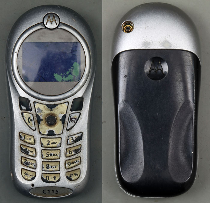
The Motorola C115 is a cell phone that uses the Calypso chipset from Texas Instruments. This model has already seen its best days, which is why it can be dismantled without feeling guilty. Cell phones with the Calypso chipset are often used to install custom software. The Osmocom project (
https://osmocom.org/) is one more widespread.
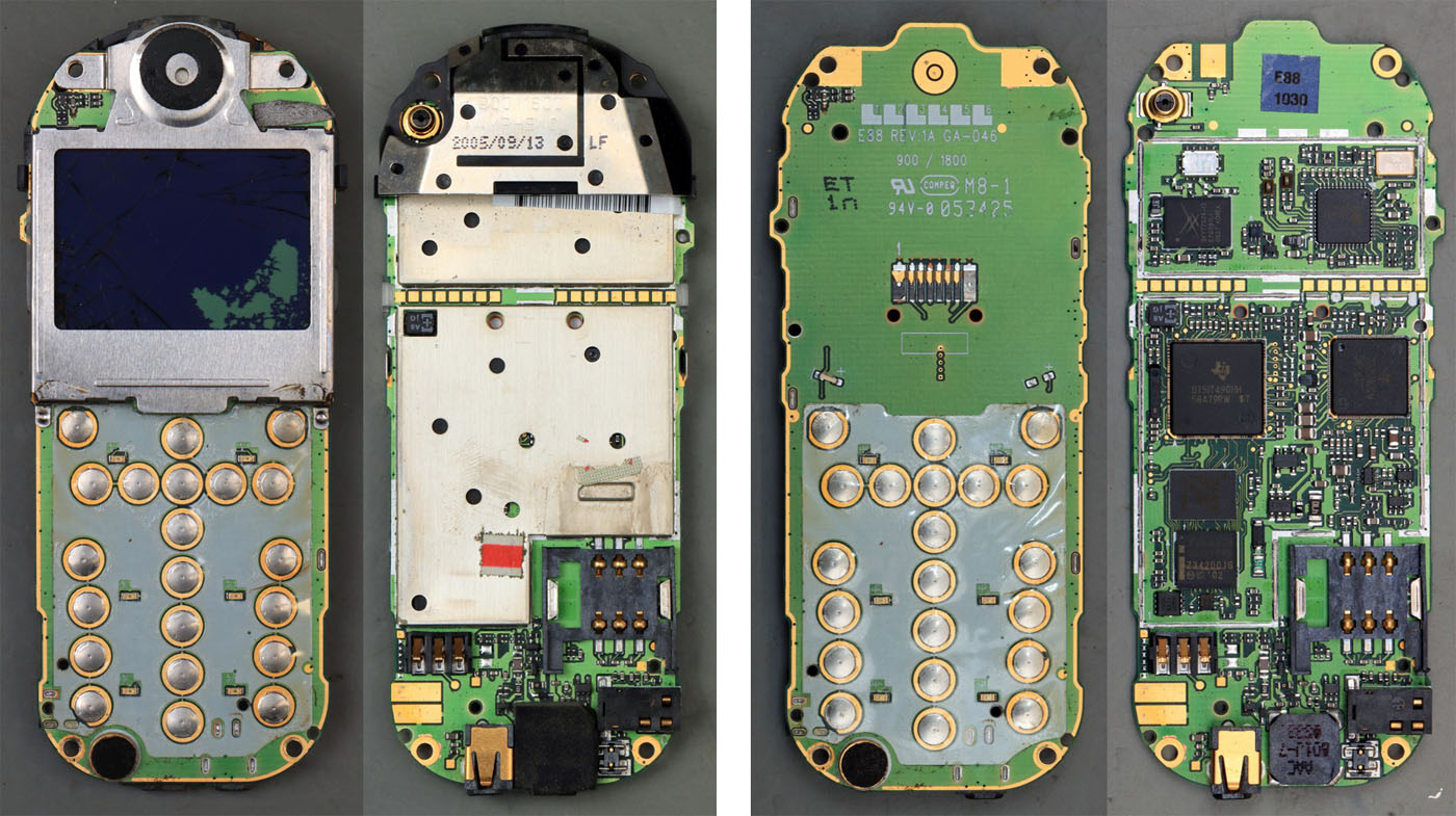
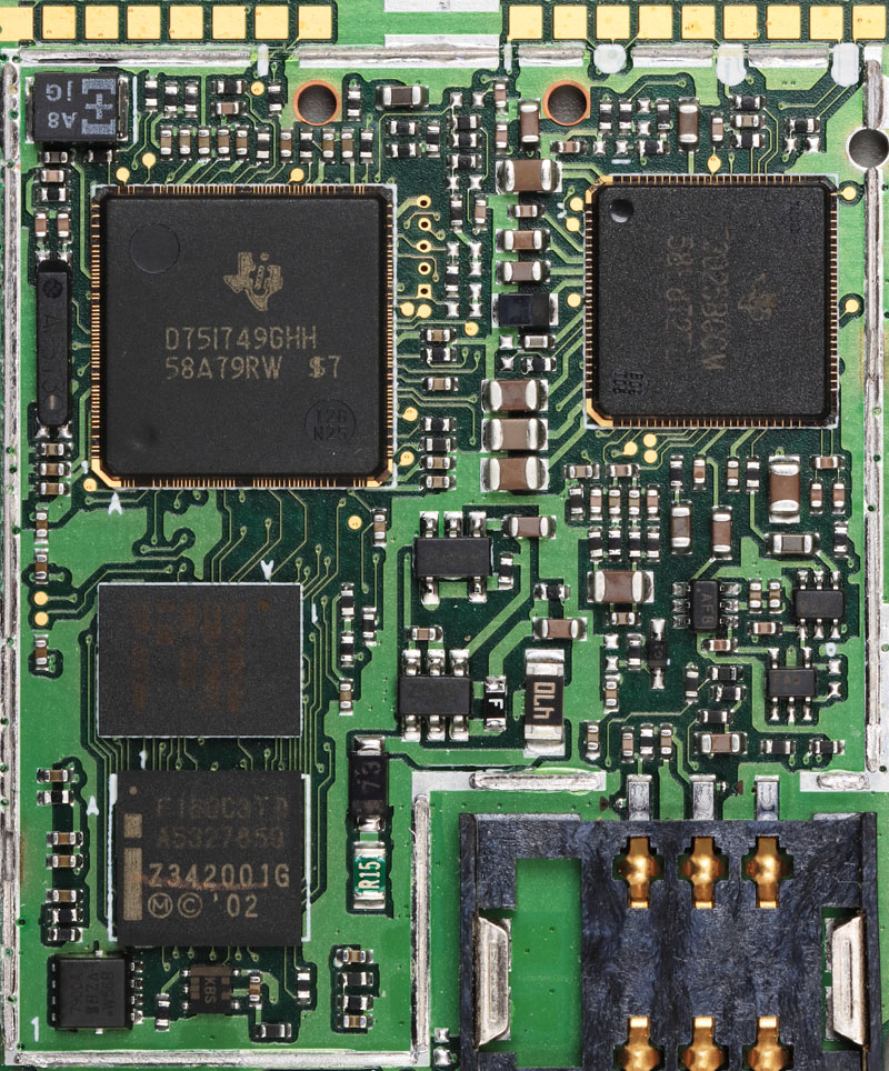
The core of the C115 is a PCB that covers the entire surface of the housing. The speaker, LCD display and keypad buttons are located on the front. On the back, in the upper area, a plastic element carries the antenna. Below this, most of the electronics are located under two shields.
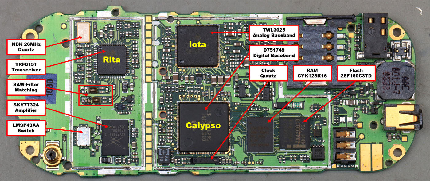
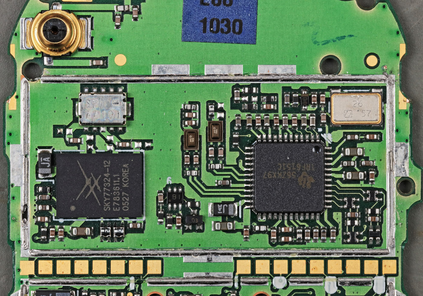
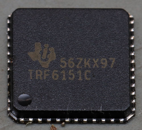
Here the core components of the circuit are marked. The antenna first leads to the Murata LMSP43AA. This switch connects the antenna to one of the two transmitters or to one of the two receivers. The SKY77324 from Skyworks is used as the transmitter amplifier. It amplifies the two possible transmission frequencies via two separate channels. Signals that are received pass through SAW filters that filter out the desired frequency range. The Texas Instruments TRF6151 is the transceiver that generates the RF signals for the transmitter from the data to be transmitted and processes the received signals so that they can be digitally evaluated. It is connected to the 26 MHz NDK NX5032SD crystal. The TRF6151 also bears the name Rita and is one of the components of the Calypso GSM chipset.
The Texas Instruments TWL3025, also known as Iota, is the analog baseband processor. It handles analog signal processing and many other functions required in a cell phone. For example, Iota controls the charging of the battery and controls the SIM card. Calypso, the Texas Instruments D751749, is the third component of the GSM chipset. It is the digital baseband processor that handles all digital functions. It contains an ARM processor and a DSP. The internal real-time clock works with a clock crystal. The pseudostatic 2MBit RAM Cypress Semiconductor CYK128K16MCCB was fitted as the main memory. The 2MB Intel 28F160C3TD flash EEPROM serves as read-only memory for the processor.
The upper shield rests on the PCB all around. The lower shield, on the other hand, has several openings. There are testpads between the two areas.
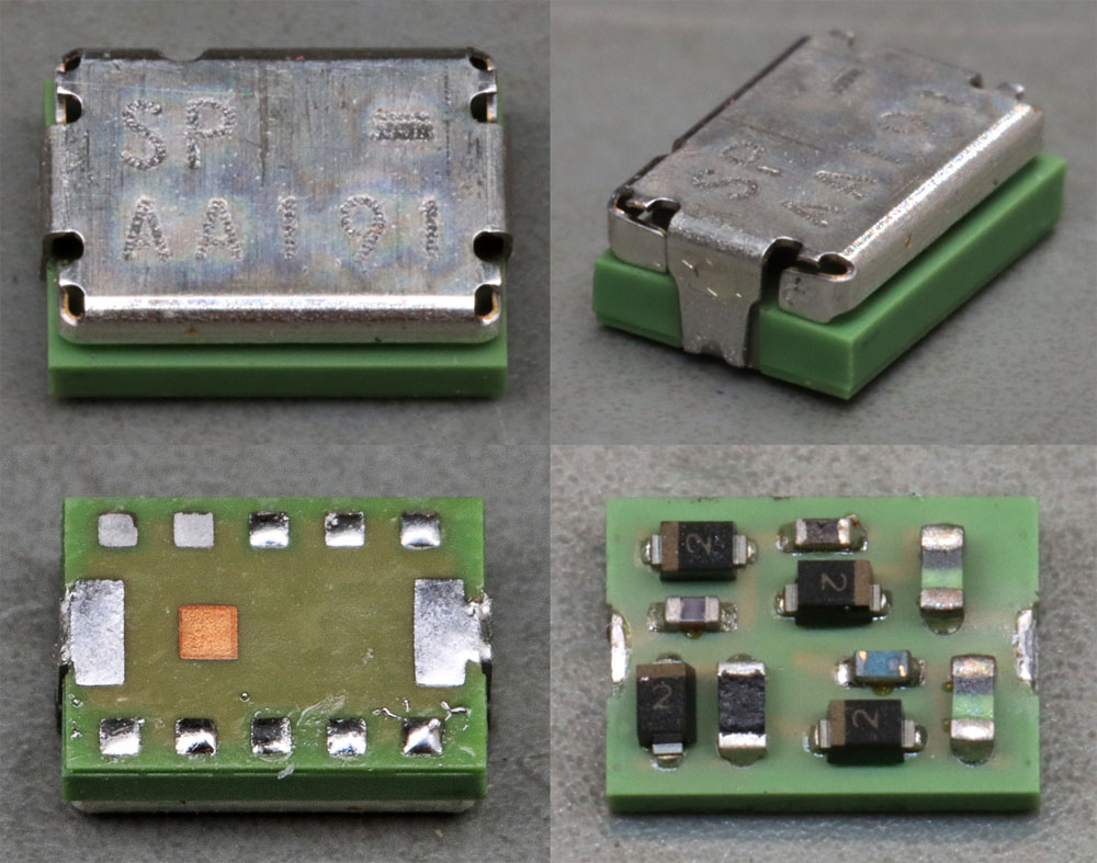
Murata refers to the LMSP43AA module as a switchplexer. It switches the antenna to one of four interfaces. These are one transmitter and one receiver path each for the frequency bands around 900 MHz and 1800 MHz. Removing the metal cover reveals four Infineon BAR64 PiN diodes operating as switches. The remaining components are probably used for impedance matching. Obviously, a special PCB material was used as circuit carrier.
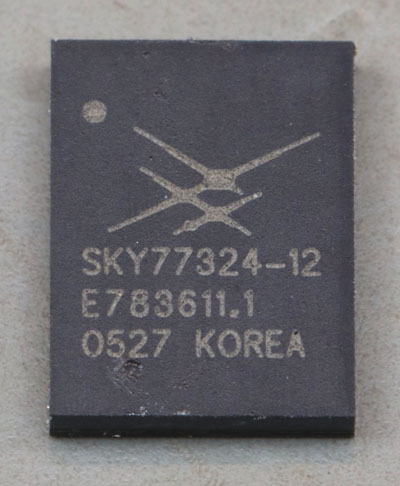
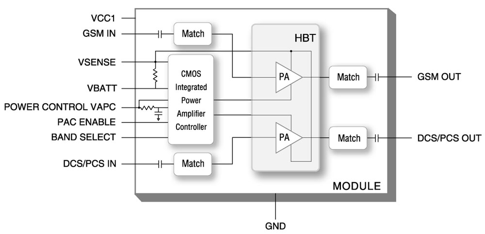
The RF amplifier used in the C115 is a Skyworks SKY77324. The block diagram already gives an indication of the structure. The two amplifiers are located in an HBT area. HBT stands for Heterojunction Bipolar Transistor. Different semiconductor materials are used within one transistor, which enables very high switching frequencies. The amplifier control, on the other hand, is implemented in a classic CMOS process. In addition, further components for impedance matching of the inputs and outputs are integrated in the package.
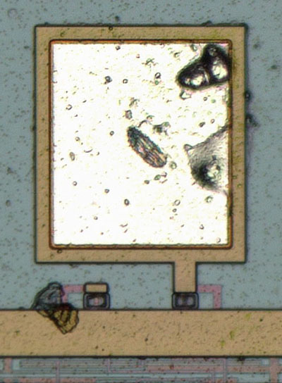
If you remove the interposer from the package, you can clearly see the many different elements. One of them is thermally connected to the large pad on the underside of the package. It can be assumed that this is the amplifier, which must be optimally cooled. The regularly arranged bondwires of a second die can be seen in the top left corner. Several SMD components are also visible.
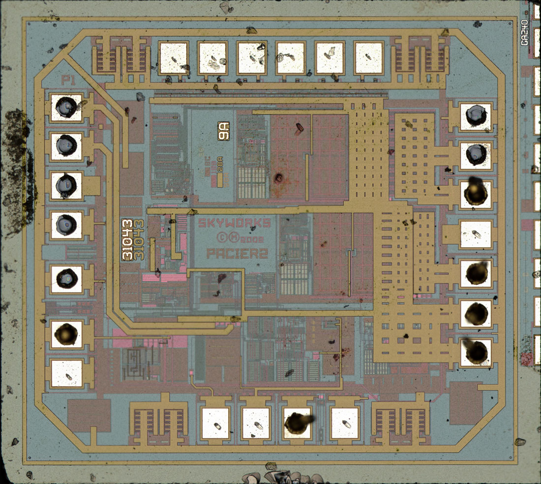
The control module is called Pacier2 and was apparently developed by Skyworks in 2002. This image is also available in higher resolution:
https://www.richis-lab.de/images/modem/02x09XL.jpg (9MB)
Classic fuses were used on the upper edge of the die.
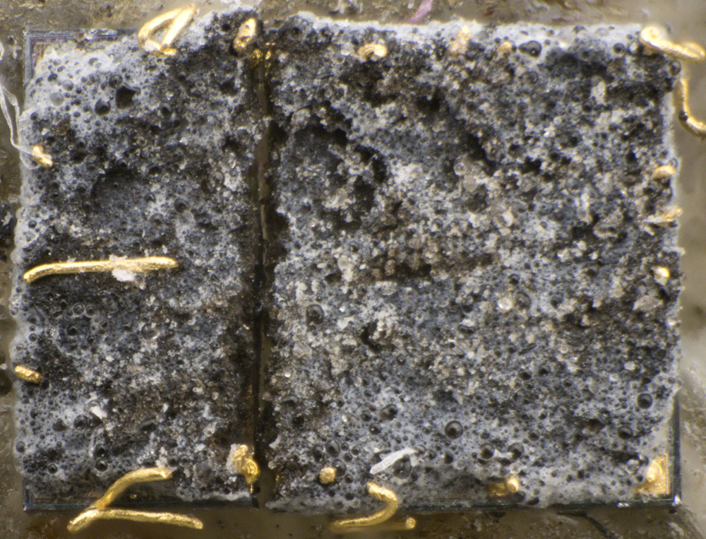
The package material sticks to the die of the HBT amplifier just as strongly as on the Skyworks SKY68001-31 (
https://www.richis-lab.de/modem01.htm#SKY68001-31). In the end, the die is broken twice and still very dirty.
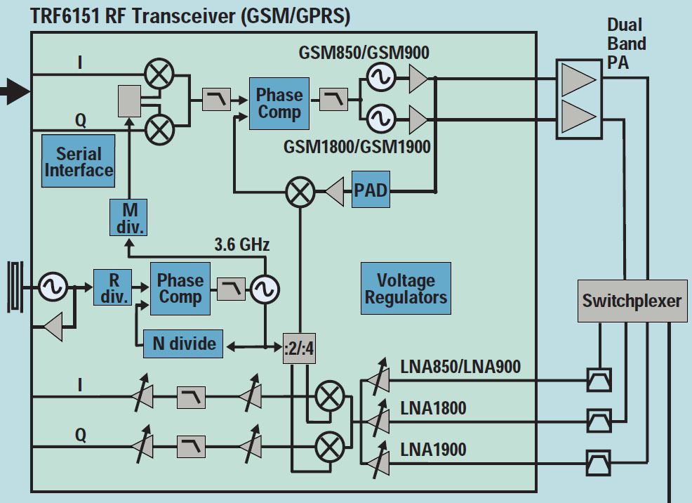
The datasheet for the Texas Instruments TRF6151 (“Rita”) transceiver is not particularly detailed. In the presentation “TCS4105 UMTS chipset solutions”, however, Texas Instruments shows a detailed block diagram. The transceiver generates and modulates the necessary frequencies. At the same time, the received signals are processed, downmixed and filtered.
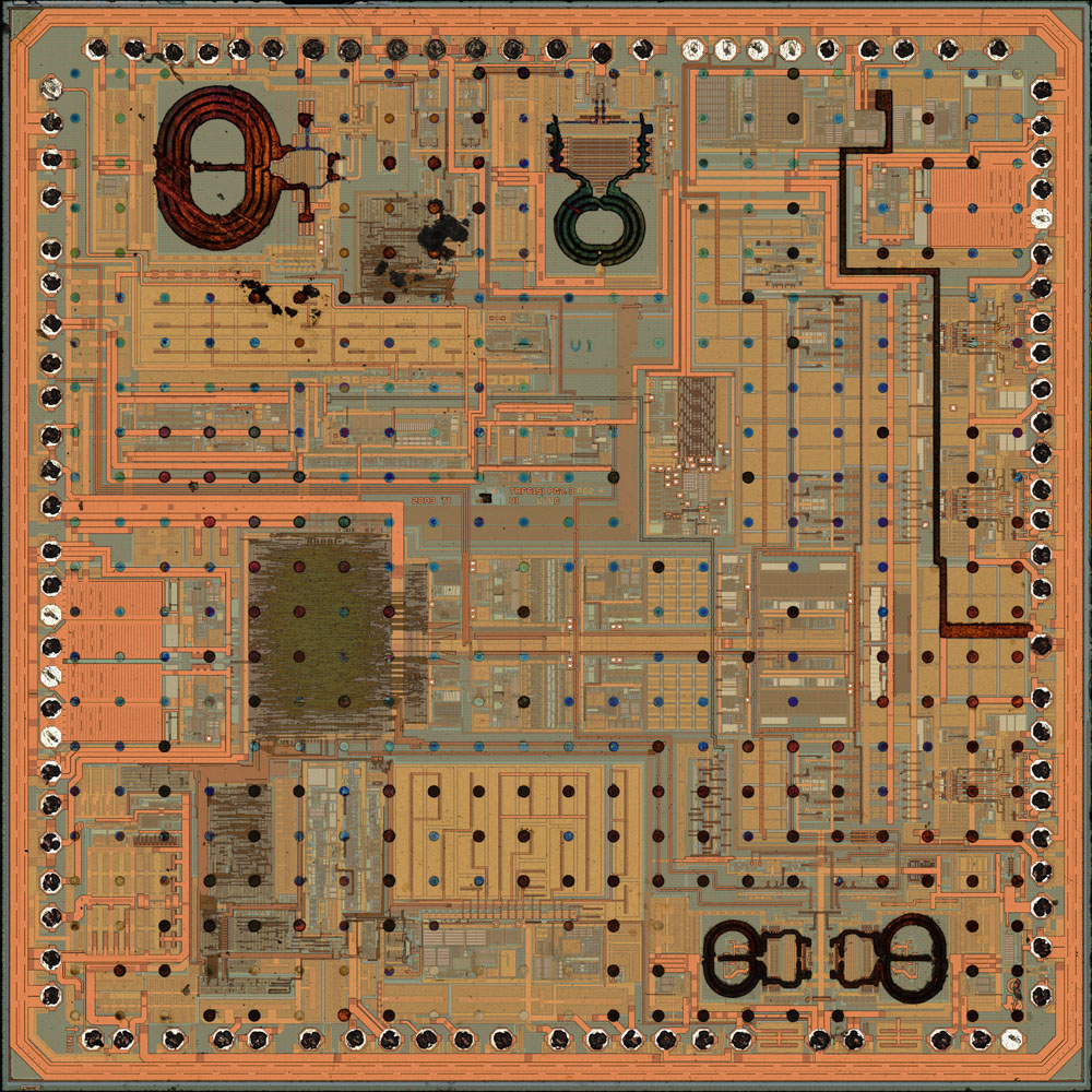
The transceiver was manufactured using the RFSIGE1 process. This is a 0,25µm BiCMOS process based on silicon-germanium and thus achieves a transit frequency of 50GHz. The top, relatively thick metal layer is immediately noticeable due to its large structures. If inductances are to be represented, as here, then the lower resistance of the thick copper layer has a positive effect on the attenuation. Dots were applied as dummy structures in the many areas where the top metal layer does not carry any conductors. This ensures more homogeneous properties of the surface.
This image is also available in higher resolution:
https://www.richis-lab.de/images/modem/02x14XL.jpg (51MB)
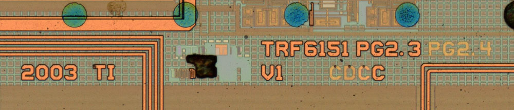
The die bears the designation TRF6151. The letters CDCC could be revisions of masks. In addition to the thick, top metal layer, the transceiver appears to have been constructed with four additional metal layers.
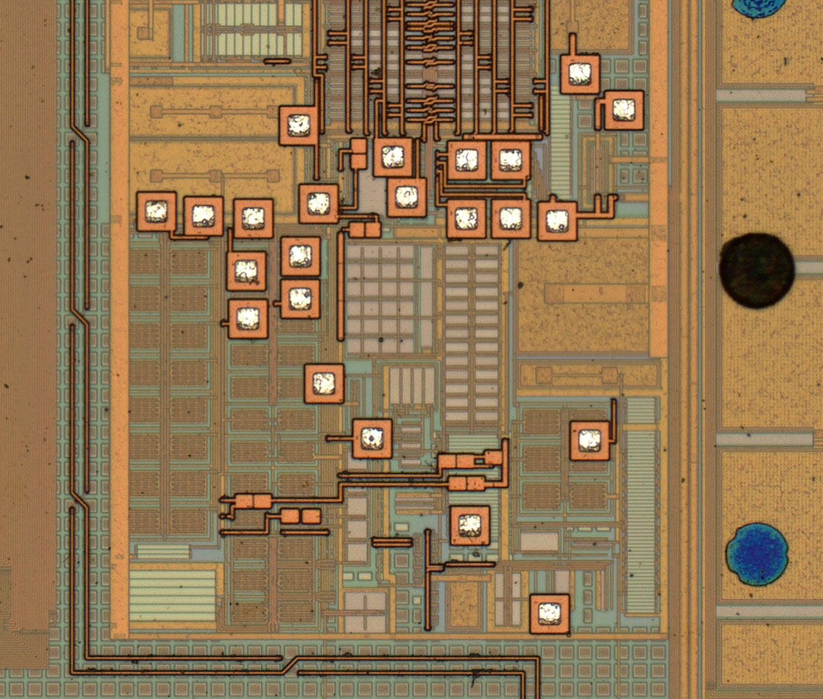
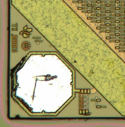
There are many small, square testpoints on the die.
The details of the circuits cannot be resolved and they are too complex for in-depth analysis. Nevertheless, the function of some structures can be guessed. Here you can see one of the three receiver paths.
The large structures on the upper edge appear to be part of the output stages. The different sizes would match the different frequencies.
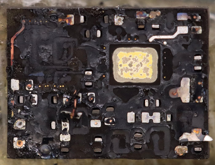
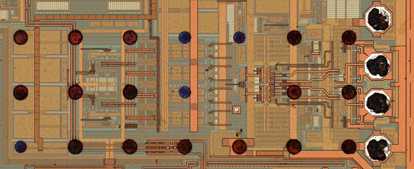
Most of the remaining circuitry is located under the second shield.
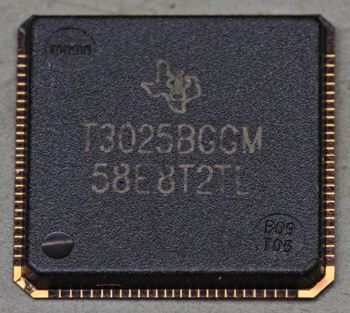
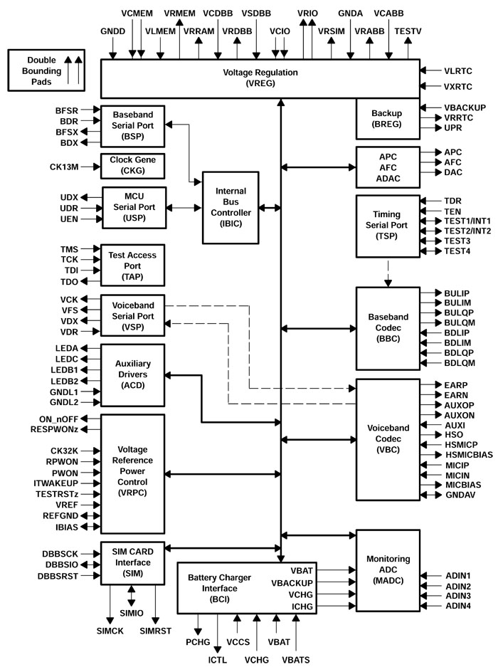
The package of the Texas Instruments TWL3025 is simply labeled T3025. It is part of the GSM chipset and bears the name Iota in this context. The TWL3025 is referred to as an analog baseband processor. However, it not only realizes the interface between the transmitter/receiver area and the classic processor of the system. Functions such as the power supply and the interface to the SIM cards are also integrated. The block diagram from the datasheet shows the various function blocks.
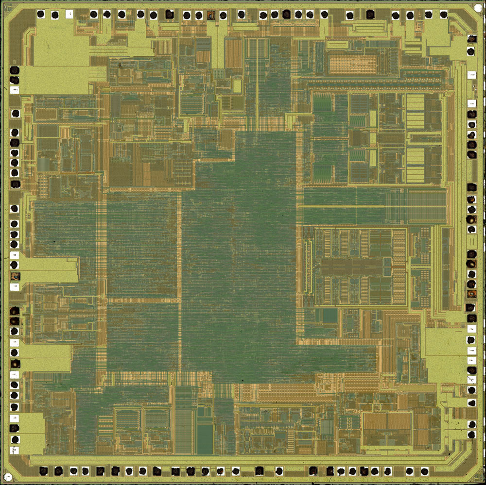
The die contains large areas of logic. However, there are also many structures that are much more heterogeneous. This image is also available in higher resolution:
https://www.richis-lab.de/images/modem/02x21XL.jpg (50MB)
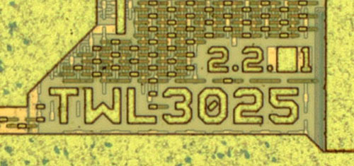
The inscription on the die shows even more clearly that it is a TWL3025. The numbers above it could indicate the revision. The free areas are filled with the dummy structures typical of Texas Instruments.
There is a copyright from 2003 in the bottom left and top right corners.
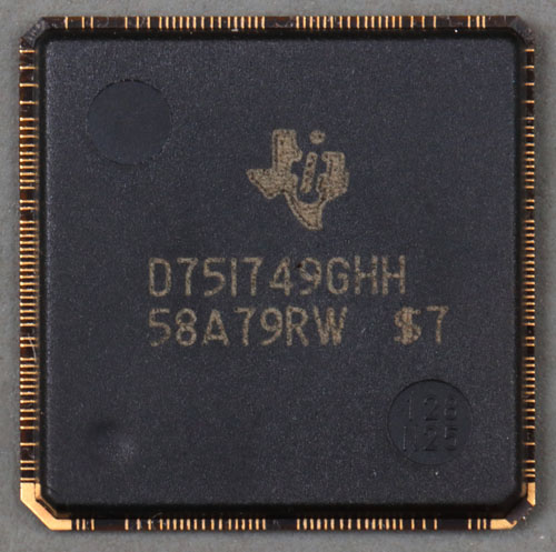
The Texas Instruments D751749GHH is the digital baseband processor and is referred to as Calypso within the Calypso chipset itself. It contains an ARM processor that controls the cell phone and a DSP for fast signal processing.
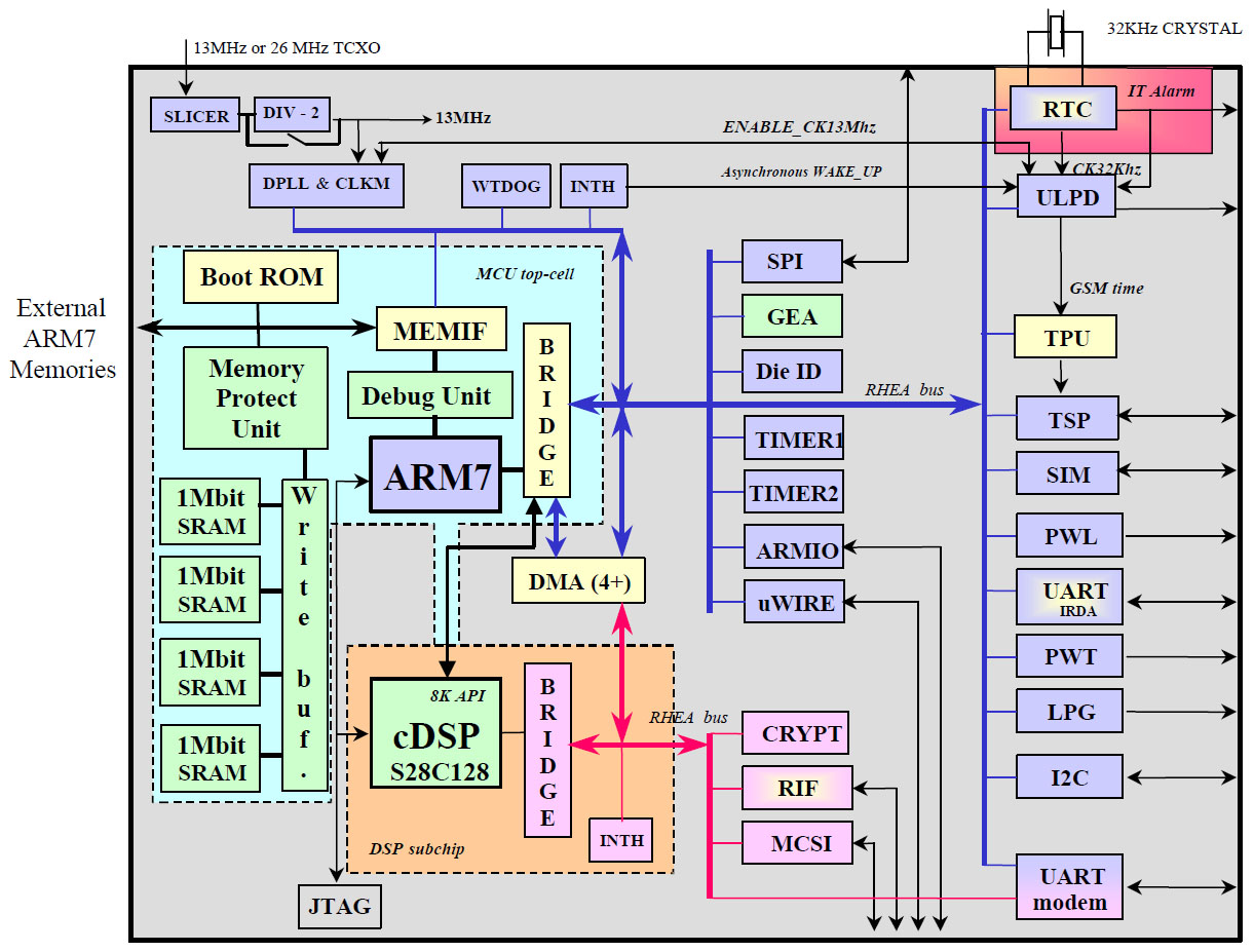
There is a detailed specification from Texas Instruments for the Calypso chip. It applies to the HERCROM400G2. This is an internal designation of the Calypso processor, of which there are different variants and development stages. The D751749GHH, for example, is always referred to as Calypso Lite G2. Even if this contains a slightly different configuration, the block diagram above still gives an impression of how the Calypso processor is structured.
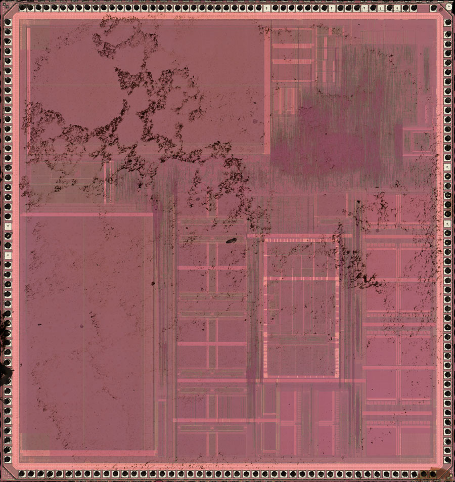
On the die of the D751749GHH one can speculate about the function of some areas, but at first glance hardly anything is clearly recognizable.
This image is also available in higher resolution:
https://www.richis-lab.de/images/modem/02x26XL.jpg (75MB)
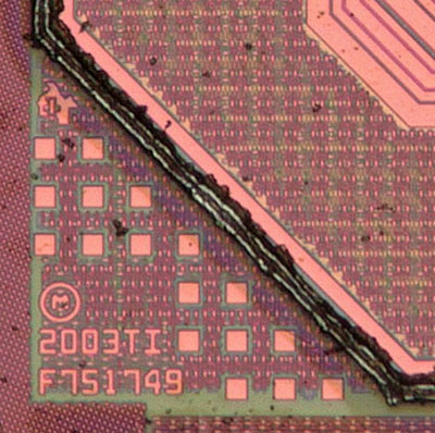
The designation F751749 is shown in the bottom left-hand corner.
https://www.richis-lab.de/modem02.htm 


