Author Topic: Different die pictures  (Read 85351 times)

0 Members and 1 Guest are viewing this topic.

Offline SYJON

  • Newbie
  • Posts: 8
  • Country: pl
Re: Different die pictures
« Reply #75 on: March 16, 2021, 09:25:14 am »
How about 555?


Offline SYJON

  • Newbie
  • Posts: 8
  • Country: pl
Re: Different die pictures
« Reply #77 on: March 16, 2021, 09:30:58 am »
Exactly! Love that  8) ;D
 

Offline Renate

  • Super Contributor
  • ***
  • Posts: 1460
  • Country: us
Re: Different die pictures
« Reply #78 on: March 16, 2021, 04:21:28 pm »
I hope that we'll get some good shots of eInk display panels soon.
Here is a (low quality) preview of a eInk "Carta" 300 DPI display driver chip.
A flex PC comes in from the top, the screen is on the bottom.
Between those two is an IC built on the glass.
This one has some sort of hard reflective cap stuck to it. It doesn't come off with a heat gun. Or a knife.
I have another one that has some sort of white silicone on top of the IC.
 

Offline NoopyTopic starter

  • Super Contributor
  • ***
  • Posts: 1730
  • Country: de
    • Richis-Lab
Re: Different die pictures
« Reply #79 on: March 23, 2021, 04:07:48 pm »


Sensitec builds some interesting current sensors that are based on the GMR effect: CDS4000 and CFS1000 for example.
They use the compensation methode. Compensating the field of the current which you want to measure.
(pictures taken from the datasheet)


Here you see a module apparently similar to the modules used in most of the Sensitec current sensors.
The small die is the GMR sensor, the big die does the signal processing.
The black blocks are magnets that gives you an offset so you can meassure positive and negative currents.


The GMR sensor is called ADK769. With this name you find some information, for example the IEEE article "High accuracy, high bandwidth magnetoresistive current sensors for spacecraft power electronics". With the help of the IEEE article we know that the two contact on the right generate the compensation field. Us1 and Us2 is the supply of the wheatstone bridge and Uo1 and Uo2 gives you the voltage proportional to the magnetic field.


The upper dark layer conducts the compensation current. The GMR elements are under the barber pole structures.
The barber pole structures are placed directly on the GMR and conduct current quite well. That gives you an angular current flow which modifies the characteristic of the GMR element so you get a linear behaviour and more sensitivity at low fields.


Here you see the current path of the compensation current.


A wheatstone bridge is quite symmetrical and robust against noise and drifts. Nevertheless Sensitec splitted the GMR elements in four parts and mixed them together probably to get it even more robust.


On the signal processing die in the upper half there is an analog part and in the lower half is a digital part.


Hello Simon!  ;D


There are four unused bondpads and 14 (!) pads each connected to something that looks quite like a fuse.


On the right side there are the big transistors for the field compensation.
The big structures on the left side could be a voltage regulator for the wheatstone bridge.


More pictures here:

https://www.richis-lab.de/hall03.htm

 :-/O
 
The following users thanked this post: daqq, brabus, doktor pyta

Offline NoopyTopic starter

  • Super Contributor
  • ***
  • Posts: 1730
  • Country: de
    • Richis-Lab
Re: Different die pictures
« Reply #80 on: April 01, 2021, 07:39:27 pm »
One step forward in the GDR digital telephone system. We have seen the NF-Filter U1001 (https://www.richis-lab.de/phone01.htm). The next IC in the line is the U1011, a Coder/Decoder which does the digital conversion respectively the analog conversion.


The resolution of the DAC and the ADC is 13Bit. These 13Bit are compressed to 8Bit what is enough for a telephone system.


The die is 5,4mm x 3,4mm.


Looks like a revision 2...


Interesting: There are "normal" testpads and smaller testpads. I assume the smaller ones were used in development.


Nice: A Switched-Capacitor-DAC


There are three transistors, one for Ref+, one for Ref- and one vor GND.


Above the GND transistor there is a fourth small transistor connecting GND with a big metal stripe. The stripe is connected to the control circuit but most notably to a big area above the GND transistor. In the next pictures we will see that this structure somehow reduces the resistance of the transistor. I assume the additional transistor modifies the body potential.


The capacitors are the same as in the U1001.


It´s a Split-Switched-Capacitor-ADC. It is split in two halfes. The MSB-DAC contains seven segments, the LSB-DAC contains six segments. The capacitor ratio is 64:32:16:8:4:2:1 then there is a small coupling capacitor and then there is the LSB-DAC with the ratio 32:16:8:4:2:2... ...well it looks like this but I´m not perfectly sure with the ...2:2.
The transistor ratios are similar but there is a change in the ratios where the additional transistor at the GND transistor comes into play.


That looks like the output opamp.


That seems to be a bias circuit for the output opamp and the comparator of the SAR-ADC. The datasheet describes an automatic offset compensation.  :-/O


It looks like they kept an option to adjust the offset from outside the die.


With nearly the same DAC they built a SAR-ADC.


Here we have two more switches for the analog signal (because you have to switch positive and negativ potentials).


That part has to be the comparator.


Interesting: In the digital part there are some small caps integrated in the substrate. It seems like the long way to the supply bondpad had to be compensated.


The digital part is too complex to analyse every function but this looks like the 13Bit/8Bit conversion.


Digital input...


...and digital output.


Here some more pictures:

https://www.richis-lab.de/phone02.htm

 :-/O

Offline NoopyTopic starter

  • Super Contributor
  • ***
  • Posts: 1730
  • Country: de
    • Richis-Lab
Re: Different die pictures
« Reply #81 on: April 08, 2021, 12:11:31 pm »


Ruhla Kaliber 15-02, a small simple digital watch.


Yeah, the battery is leaking a little.  ;D


With the small capacitor at the bottom of the board you can tune the clock.
The quartz is missing.


Here we see the contact rubber for the lcd.
They drilled two holes between the lcd and the capacitor cutting some traces. They needed this connection to galvanise the board with gold. That also a cause for the traces leading to the edge of the board.
There are some interesting dendrites at the capacitor. Perhaps because of the electrolyte?


The LCD...


They potted the controller into the PCB.
After bonding the die they took a black lid on top of the board. The bondwires get bent but it seems that was no problem.


The die is coated (2,9mm x 2,8mm).


The service manual states the controller is a KB1004CHL5-4. Probably it´s a КБ1004ХЛ5-4. Russia had a lot of clock controllers have a 1004ХЛ in their name.


A lot of the area is occupied by some similar structures, probably the lcd drivers.


There are strange structures in the middle of the die. Perhaps that is something like a mask programmed melody generator for the alarm.


https://www.richis-lab.de/clock01.htm


 :-/O

Offline NoopyTopic starter

  • Super Contributor
  • ***
  • Posts: 1730
  • Country: de
    • Richis-Lab
Re: Different die pictures
« Reply #82 on: April 12, 2021, 08:05:50 pm »
As part of the GDR digital telephone system we have seen the filter circuit U1001 (https://www.richis-lab.de/phone01.htm) and the PCM-coder/decoder (https://www.richis-lab.de/phone02.htm). Now here we have the U1500PC050 which controls the signal flow.


The die is 5,9mm x 5,9mm.


The U1500PC050 is based on the Zeiss U1500. With the U1500 system you can built an ASIC out of standard cells.


Some structures to check the process quality.


The U1500PC050 was designed in the "Institut für Nachrichtentechnik".


The input bondpads are connected to the clamping diodes with a series resistor. The signal is buffered in a push-pull-stage and then reaches the internal circuit.
Around the bondpads there seems to be some kind of additional isolation.


A small push-pull output stage.


There are five bigger output stages. Different to the smaller output stages the highside and the lowside transistor are controlled with two lines. There is probably a tristate mode. That makes sense because there is also an input circuit connected to these output stages.


There is an exclusive supply bondpad at the big output stages.


In the logic block we find the same capacitors as in the U1011 (https://www.richis-lab.de/phone02.htm).


https://www.richis-lab.de/phone03.htm

 :-/O
 
The following users thanked this post: RoGeorge

Offline NoopyTopic starter

  • Super Contributor
  • ***
  • Posts: 1730
  • Country: de
    • Richis-Lab
Re: Different die pictures
« Reply #83 on: April 17, 2021, 07:34:19 pm »
Today I have a special Fluke analog switch for you. There was already a thread about it so I placed the pictures there:

https://www.eevblog.com/forum/testgear/replacement-for-fluke-700013-ic-(quad-spst-analog-switch)/msg3551343/#msg3551343

 :-/O

Offline NoopyTopic starter

  • Super Contributor
  • ***
  • Posts: 1730
  • Country: de
    • Richis-Lab
Re: Different die pictures
« Reply #84 on: April 23, 2021, 08:23:15 pm »


The NEC µPD7220 is the world´s first graphic processor. The µPD7220A is the second generation.
The µPD7220AD is the ceramic package. -2 stands for the fastest version. Probably they did some binning.


The die is 4,3mm x 4,3mm. The datasheet explains that a NMOS process was used.
In the 1981 IEEE International Solid-State Circuits Conference the µPD7220 was introduced. The first generation had a die size of 7mm x 7mm. They did quite some shrinking to get to the µPD7220A.


Designed 1983...


HGDC? Some enigneers?


Some test structures...


The computer system bus and the graphic memory bus IOs are equipped with their own ground rail that is connected to the package ground with two bondwires.


And three more ground wires for the rest of the logic.


The memory blocks are easy to spot. On the right side there is the FIFO buffer (16x9) and the parameter RAM (16x8). On the left side there is the instruction ROM (128x14).


Some more pictures here:

https://www.richis-lab.de/GraKa01.htm

 :-/O
 
The following users thanked this post: RoGeorge

Offline NoopyTopic starter

  • Super Contributor
  • ***
  • Posts: 1730
  • Country: de
    • Richis-Lab
Re: Different die pictures
« Reply #85 on: May 12, 2021, 06:48:25 pm »
Here we have the next part of the GDR telephone system (https://www.richis-lab.de/phone.htm), the B384 which regulates the voltage of the subscriber's extension.


The datasheet shows the B384 as a switching regulator. The output voltage depends on the control signals RU, HR, BR.
There is a small mistake in the schematic. Can you find it? (answer at the end)
There is also an overvoltage protection circuit which activates an external thyristor with 5mA independent of the actual voltage.


The die is 4,3mm x 3,4mm. The integration density is quite low...


...that´s because the circuit has to withstand 100,25V (yes, that´s the value in the datasheet  ;D). There is quite some room between the transistors. Around the transistor structure itself there is a reddish line connected to the collector. I assume that´s some kind of potential steering to get a uniform electric field.  :-//


Some parts are integrated in squares where the distances are smaller. In these squares the voltages are lower.


There are some spare parts on the die.


Now that is interesting: There are some metal lines on the die. On one side these lines are connected to the substrate. On the other side there is a bigger area which isn´t connected to anything. I don´t know what these metal lines do!  :-//


The driver for the thyristor overvoltage protection consists of six transistors but only one of them is connected. Probably they connected the number of transistors they needed to get the right driver current. Nevertheless it´s strange there is only one of six connected.
There are two diodes (only one connected) which probably protect the base emitter junction of the driver transistor.


The driver transistors are darlington transistors.


Here we see the two power transistors and the two freewheeling diodes of the switching regulator.
Under the bondpad Ucc4 is the current limiter.
Aaaaaand the mistake in the schematic is the freewheeling diode at the bondpad L1. In the schematic it has the wrong polarity. It would create a short if the Ucc4-transistor switches.


https://www.richis-lab.de/phone04.htm

 :-/O
 
The following users thanked this post: RoGeorge

Offline NoopyTopic starter

  • Super Contributor
  • ***
  • Posts: 1730
  • Country: de
    • Richis-Lab
Re: Different die pictures
« Reply #86 on: May 16, 2021, 11:10:19 am »


Intersil ICM7045, a circuit to control a digital clock (also good for building a timer or stopwatch). The supply voltage should be between 2,5V- 4,5V. The power consumption is just 0,9mW. The ICM7045 can drive up to eight 7-Segment-LED-Displays.


The die is 3,3mm x 3,4mm.
In the centre of the die there is the logic counting the seconds, minutes, hours and controlling the display. At the edges of the die there are the big transistors that conduct the current flowing through the LED display.


ICM7045T is the internal naming of the design. As we have seen on other Intersil dies T is the revision that started at Z.
6C is the revision of the metal layer mask.
Under the metal frame we can see some other mask revisions: 1A, 2A, 3A, 5XA und 7A.


Coloring the power supply traces the location of highside and lowside drivers come into view.


Datasheet states that the ICM7045 was fabricated with a metal gate CMOS process. Here we see the metal rectangles acting as gates for the output transistors. Under the metal there are the intermeshing drain and source.


The epoxy of this older ICM7045 is a little short.  :-//


The design is the same...


https://www.richis-lab.de/clock02.htm

 :-/O
 
The following users thanked this post: RoGeorge

Offline NoopyTopic starter

  • Super Contributor
  • ***
  • Posts: 1730
  • Country: de
    • Richis-Lab
Re: Different die pictures
« Reply #87 on: May 17, 2021, 12:42:50 pm »
...
Ruhla Kaliber 15-02, a small simple digital watch.
...


They potted the controller into the PCB.
After bonding the die they took a black lid on top of the board. The bondwires get bent but it seems that was no problem.
...


I found a picture showing how the board and the ic look like before "closing the hatch":


It´s not exactly the same clock but it´s quite similar.


https://www.richis-lab.de/clock01.htm

 :-/O

Offline NoopyTopic starter

  • Super Contributor
  • ***
  • Posts: 1730
  • Country: de
    • Richis-Lab
Re: Different die pictures
« Reply #88 on: May 17, 2021, 01:24:57 pm »


It´s not exactly the same clock but it´s quite similar.


Sorry, I have to correct myself: That´s an older stage of development. Here the die is on the board, not in the board. The die got potted in the next step but it´s not placed in the board.

Offline NoopyTopic starter

  • Super Contributor
  • ***
  • Posts: 1730
  • Country: de
    • Richis-Lab
Re: Different die pictures
« Reply #89 on: May 25, 2021, 02:23:53 pm »
Let´s take a look into a digital audio amplifier!


TDA8920, a well known 2x110W (+/-27V, 3Ω, 10% THD) amplifier built by Philips (today NXP).
It´s a nice SMT-package with a metal plate for top cooling.


On the heatsink we have the die with some gel potting.


The die is 5,1mm x 4,2mm. We can clearly see the two channels. It´s also no problem to spot the power transistors in the lower area.


Already NXP...


The low power part is too high integrated to analyse every part of the circuit but we can see the differential inputs left and right on the upper edge of the die. The first three bondpads leading downwards left and right are VDDA, SGND and VSSA for each channel. In the middle there must be some control circuit.


Each channel has two big capacitors and two huge resistors!  :o


Well that are clearly logic lines like in a gatearray.


I assume the smaller circuits above the power transistors contain the driver and protection. It would be a logical location and the bootstrap supply ends here.


The line between the two power stages seems to contain a small power transistor. At the end of the line you have to connect the capacitor for the internal power supply. Probably that power transistor is a linear regulator.


Each Push-Pull-Stage uses six highside blocks (red/green) and six lowside blocks (green/blue). The output and the supply each use three bondwires.
At the lower edge there is the bootstrap circuit.


The power transistor structures are too small to analyse them in detail.


For the bootstrapping there is a diode connected to BOOT and leading to a exclusive VDD bondpad. The brown rectangle probably contains a low value resistor to damp the charge process of the bootstrap capacitor.
I assume the thing between BOOT and OUT is a zener to cut overvoltages at the bootstrap capacitor that can occur due to parasitic inductance at the output.


https://www.richis-lab.de/audioamp05.htm

 :-/O
 
The following users thanked this post: brabus, RoGeorge

Offline NoopyTopic starter

  • Super Contributor
  • ***
  • Posts: 1730
  • Country: de
    • Richis-Lab
Re: Different die pictures
« Reply #90 on: June 02, 2021, 06:37:43 pm »
Here we have the next part of the GDR telephone system (https://www.richis-lab.de/phone.htm), the B385, a test circuit:


Just some switches for the telephone wires. But these are interesting switches. They integrated thyristor switches which can withstand 91V, conduct 70mA and guarantee a on resistance of 17 \$\Omega\$.


The die is 3,1mm x 4,1mm.
You can clearly see the six switches and their control circuits.


To allow bidirectional current flow there are two thyristor switches connected antiparallel.
Interesting structures...


https://www.richis-lab.de/phone05.htm

 :-/O

Offline NoopyTopic starter

  • Super Contributor
  • ***
  • Posts: 1730
  • Country: de
    • Richis-Lab
Re: Different die pictures
« Reply #91 on: June 04, 2021, 11:41:25 am »

Offline NoopyTopic starter

  • Super Contributor
  • ***
  • Posts: 1730
  • Country: de
    • Richis-Lab
Re: Different die pictures
« Reply #92 on: June 08, 2021, 03:41:37 am »


MAX232A, a RS-232 line driver/receiver with an integrated charge pump.
The MAX232A is the newer revision of the MAX232 and needs less capacitance.


The die is 2,9mm x 1,8mm.


Built 1986.


Identifying the functional blocks is no bigger problem (sorry, german  ;)).
On the right side you have the two inputs and the two outputs.
On the left side there are the charge pumps.


At the input there is a big resistor (Ro) building a voltage divider with the resistor Ru. You can spot the lowside, the highside, the driver and the feedback circuit.


The input resistors have to be isolated better because the input voltage can go up/down to +/-25V.
The metal layer makes it possible to adjust the resistance with two fuses. With two more fuses they were able to adjust the lower resistor of the voltage divider.
The numbers seem to be mask revisions.


Here we have the lower resistor of the voltage divider, the input and the feedback resistor. The feedback resistor can be adjusted by changing the metal layer.


Between the input signal and the feedback there are two clamping diodes.


Below the RS-232-input there is the RS-232-output circuit.


Here we have the first charge pump. Four transistors switch the capacitor C1 to the +5V-supply to charge it to +5V. Then the capacitor is connected "on top of the +5V supply" and you get +10V at "V+".


In the second charge pump four transistors charge the capacitor C2 to +10V and switch it reversed to GND which gives us -10V at "V-".  :-+


https://www.richis-lab.de/transceiver01.htm

 :-+
 
The following users thanked this post: edavid, RoGeorge

Offline NoopyTopic starter

  • Super Contributor
  • ***
  • Posts: 1730
  • Country: de
    • Richis-Lab
Re: Different die pictures
« Reply #93 on: June 14, 2021, 03:35:11 am »


BQ27220, a single li cell fuel gauge in a small flip-chip package (DSBGA-9 - 1,62mm × 1,58mm).


Flip-chip, the die gets the solder balls on top of it and is flipped to solder it on the board.


It looks like there is a thin coating on top of the BQ27220. Flip-chip parts often have problems with light fluctuations. Some time ago there was a flip-chip voltage regulator on a Raspberry Pi 2 that resets the processor whenever you take a picture of the board using a flashlight.  :o Perhaps this coating damps some of the light reaching the chip.


Due to the used optics it looks like the solder balls get bigger in the background. That´s not true.  ;D


You don´t see much of the circuit but the area in the upper left corner looks like logic. The area in the lower left corner looks like memory. The BQ27220 has quite some memory.


https://www.richis-lab.de/li01.htm

 :-/O
 
The following users thanked this post: doktor pyta, RoGeorge

Online RoGeorge

  • Super Contributor
  • ***
  • Posts: 6187
  • Country: ro
Re: Different die pictures
« Reply #94 on: June 14, 2021, 02:20:00 pm »
Due to the used optics it looks like the solder balls get bigger in the background. That´s not true.  ;D

They all have about the same number of pixels in diameter, yet the brain assumes the usual 3D to 2D geometric projection, therefore brain concludes the further away ones should be bigger.   ::)

After I explained to brain what happened, brain still concludes the back ones are bigger.   :palm:
 
The following users thanked this post: Noopy

Offline NoopyTopic starter

  • Super Contributor
  • ***
  • Posts: 1730
  • Country: de
    • Richis-Lab
Re: Different die pictures
« Reply #95 on: June 20, 2021, 08:54:59 pm »


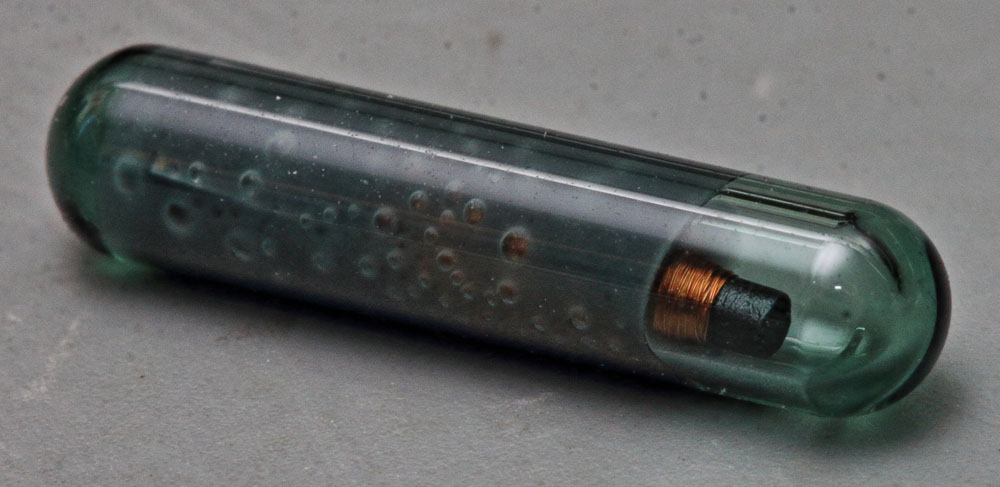
Let´s take a look into a immobilizer transponder as it is used a lot in older generations of cars. The transponder is put into the key and a coil in the car communicates with the transponder to check if the key is valid.
The transponder contains a chip and an inductance which is potted in something like silicone.


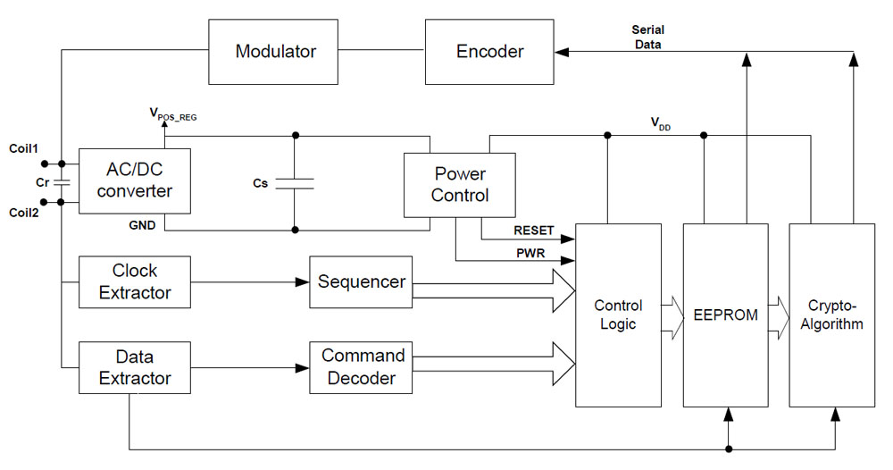
The datasheet of the EM4170 (the immobilizer chip) shows the building blocks of the chip.
There is a resonance capacitor on the die. A AC/DC converter draws energy from the antenna and charges a capacitor to 9,5V at maximum. A voltage regulator supplies the logic with 3,5V.
Clock and data are extracted from the antenna and fed to the logic.
There is an 16x16-EEPROM with a read only 96Bit secret key, a 32Bit unique ID and 94Bit User Memory. The memory is protected with a 32Bit PIN.
The crypto algorithm seems to be in a separate block.
The transponder communicates with the transceiver by damping the antenna which modulates the voltages at the antenna of the transceiver.


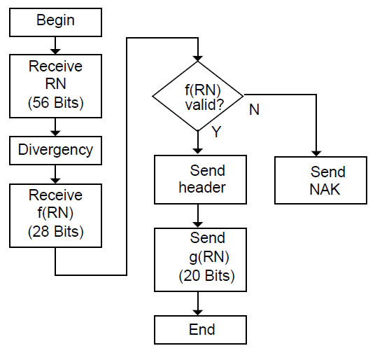
The datesheet gives us a small glimpse into the authentication process. The transceiver sends a random number and a encrypted variant of this number. If the transponder calculates the same numbers it gives feedback and sends another variant of the random number which authenticates the transponder.


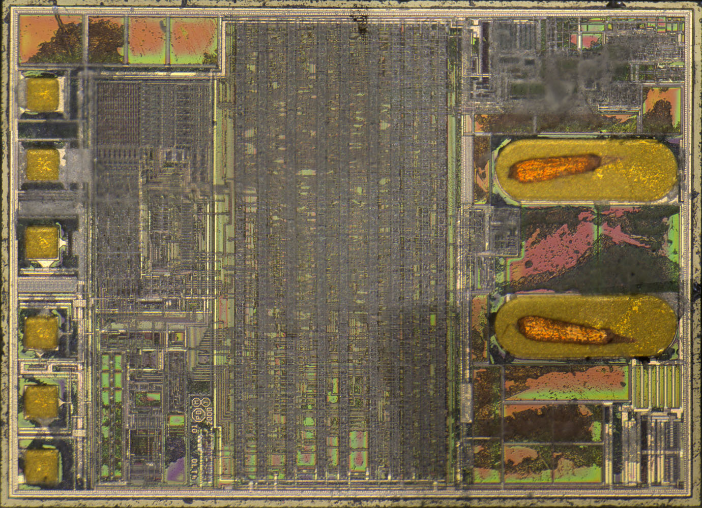
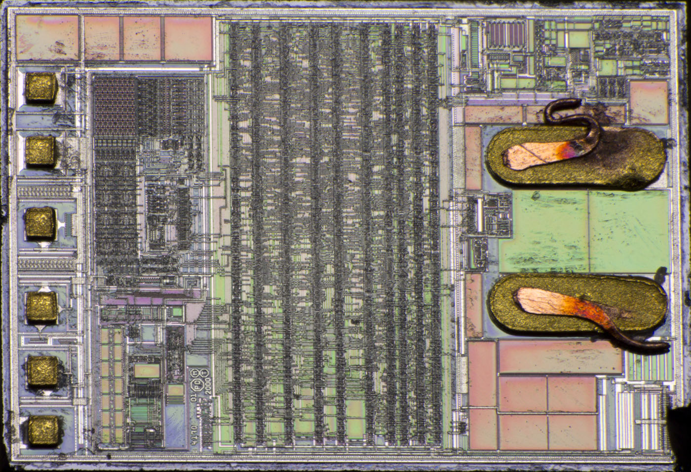
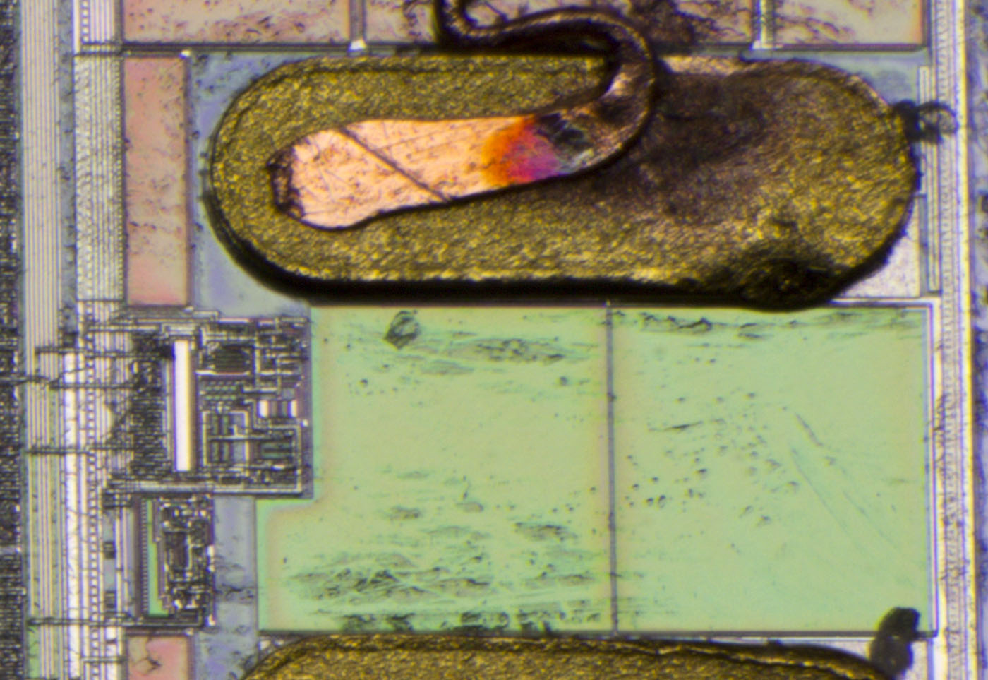
The die is 2,3mm x 1,7mm. You contact the ferrite coil at the right two bondpads. On the left edge there are some testpads. I assume with this testpads the unique ID is written.


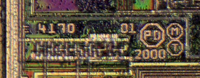
The design of the EM4170 dates back to the year 2000.


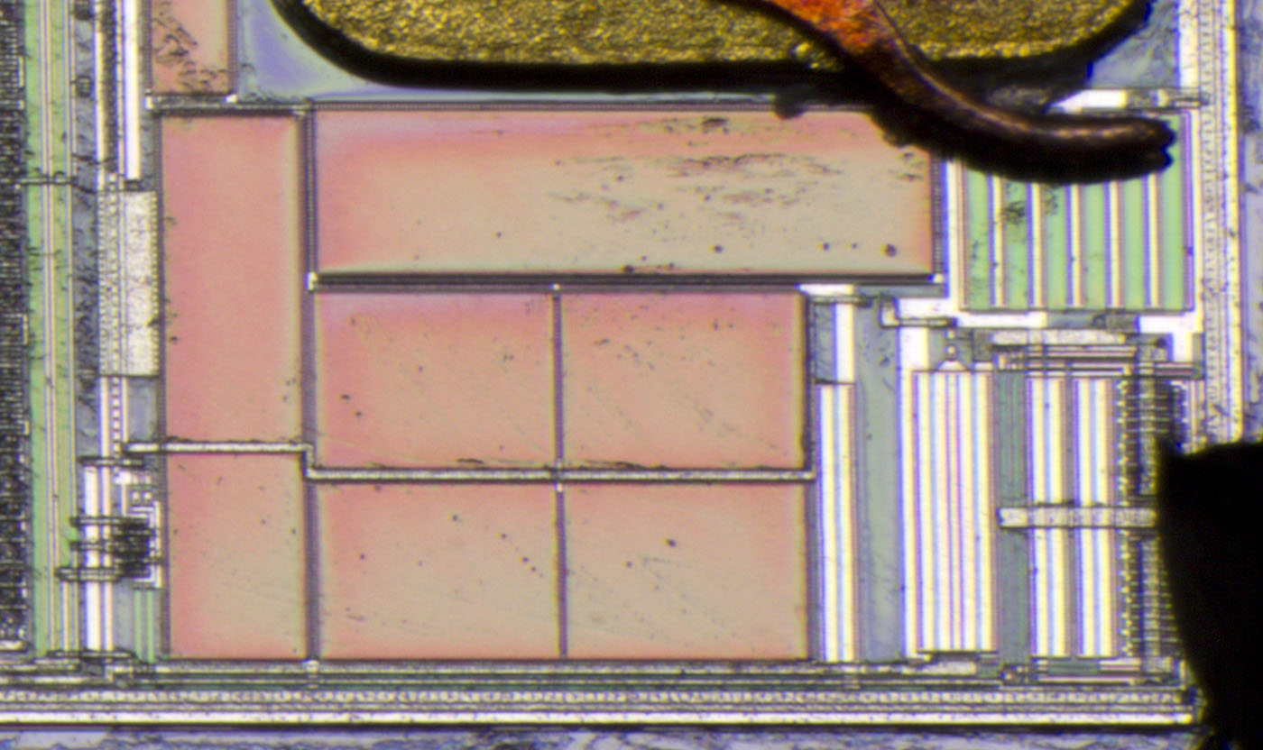
On the right edge there are a lot of capacitors, a lot of them probably acting as resonance capacitors.
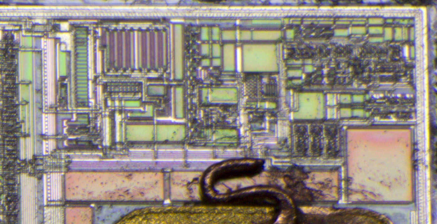
In the upper area there are smaller structures, probably data and clock generation.
In the lower right corner there are bigger structures. Perhaps that´s the damping circuit that modulates the data into the electromagnetic field.


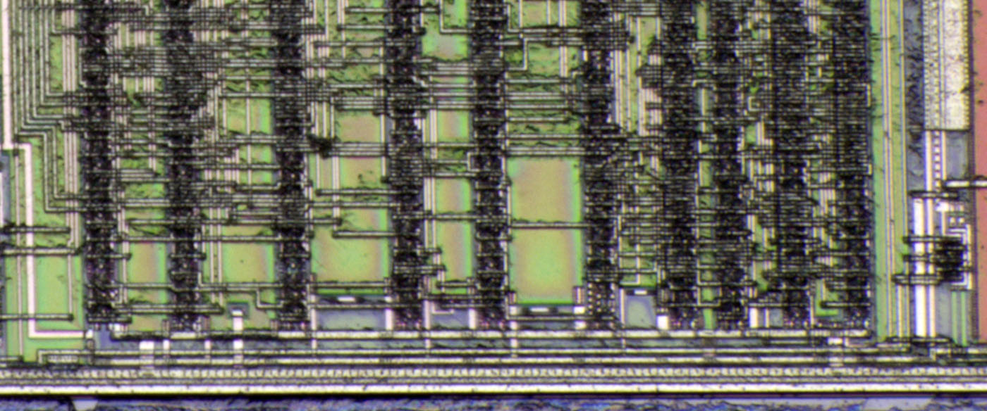
In the middle of the die there is some standard logic. You can see the lines with the standard cells and the interconnection between them.


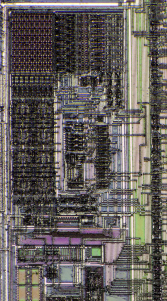
Here we have the memory area.


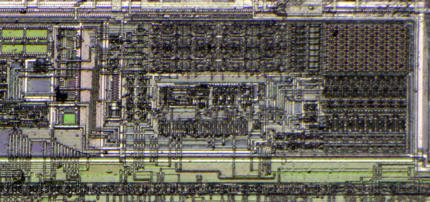
In the lower left corner you can see 18 lines coming out of the logic area. In the upper area there are 16 lines leading towards the memory. That fits good with the 16x16 memory.
In the upper right corner there is the symmetric structure of the memory. It´s interesting that there is a very big and dense area left of the memory. I assume in this area there is most of the cryptographic algorithm.


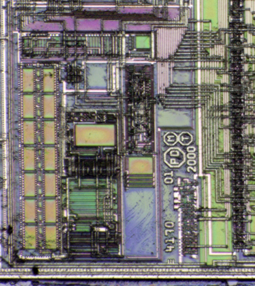
There is another circuit with capacitors under the memory area. I assume that is the "high voltage" generator that is necessary to write into the EEPROM.


https://www.richis-lab.de/transponder01.htm

 :-/O
 
The following users thanked this post: SeanB, RoGeorge, Jo

Offline NoopyTopic starter

  • Super Contributor
  • ***
  • Posts: 1730
  • Country: de
    • Richis-Lab
Re: Different die pictures
« Reply #96 on: June 24, 2021, 04:02:56 am »
Here we have the next part of the GDR telephone system (https://www.richis-lab.de/phone.htm), the B386, a test circuit:


The B386 supplies the telephone line with the necessary voltages (supply, ringing,...).


The circuits of the B386 keep some distance between them to isolate the high voltages.
There are quite some unused circuits.


The output amplifier use the same transistors as we have seen in the B384 (https://www.richis-lab.de/phone04.htm). The output stage is quasi complementary.
There are four big capacitors. The outer capacitors are unused the inner capacitors seem to represent a bootstrap circuit.


https://www.richis-lab.de/phone06.htm

 :-/O
 
The following users thanked this post: RoGeorge

Offline NoopyTopic starter

  • Super Contributor
  • ***
  • Posts: 1730
  • Country: de
    • Richis-Lab
Re: Different die pictures
« Reply #97 on: June 28, 2021, 08:04:23 pm »
Now I have a µPD7220 completing the µPD7220 pictures. Let´s do some comparisons:


The older die is 5,3mm x 5,2mm, the newer die is 4,3mm x 4,2mm. The structures are quite similar. The most significant difference are two exclusive ground lines for the two big interfaces (see µPD7220A: https://www.eevblog.com/forum/projects/different-die-pictures/msg3555753/#msg3555753).
http://www.oguchi-rd.com/ states that the smallest feature size of the µPD7220 was 3µm. With the scaling of the dies we can estimate that the µPD7220A was fabricated with a 2,5µm process.


 :-+


"Graphics Display Controller" vs. "High Performance Graphics Display Controller" They barely changed something. ;D
But the clock frequency specification war risen: 4MHz, 5Mhz and 5,5MHz vs. 6MHz, 7Mhz and 8MHz. Probably the smaller structures did a lot of the job.


In the µPD7220 there is kind of a test circuit on the die. The circuit isn´t connected to anything but there are two rectangles which could be used for test needles. Perhaps it´s kind of an oscillator showing the fabrication quality.


The bigger structures make it easier to study the memory areas.
Here we see the control ROM. It´s not 128x14 but 65x32.  :-/O ;D


You can find some more pictures here:

µPD7220:
https://www.richis-lab.de/GraKa02.htm

µPD7220A:
https://www.richis-lab.de/GraKa01.htm


 :-/O
« Last Edit: June 28, 2021, 08:15:48 pm by Noopy »
 
The following users thanked this post: SeanB, RoGeorge

Offline NoopyTopic starter

  • Super Contributor
  • ***
  • Posts: 1730
  • Country: de
    • Richis-Lab
Re: Different die pictures
« Reply #98 on: July 02, 2021, 08:35:02 pm »


MAX7219, a 7-segment driver controlled over a serial bus with up to 10MHz.


The die is 1,2mm x 1,1mm.


In the datasheet there is a picture of the die but that looks quite different. Perhaps that is the die of the MAX7221. The MAX7221 has a lower slew rate at the outputs and switches from active to tristate not to the opposite potential. The MAX7221 also can directly work on a SPI bus.


A first revision?
LTH6868?


In the upper area you see the digit drivers making 320mA each. There are two big lowside transistors around each bondpad. You can spot a big wire connecting the bondpad to the inner supply line where the smaller highside transistors switch to a high level with 2mA.


In the lower area there are the segment drivers delivering 40mA each. In the middle you see the supply bondpad and left of it is the bondpad for LED current adjustment. At this bondpad there is a thick wire leading upwards. At the edge of the die there are small lowside transistors conducting 5mA while the segment is disabled. In the inner line there are the highside transistors acting as current sources. The highside transistors are half the size of the lowside transistors but can only conduct a little more than 1/10 of the current.


Inputs - The big structures are probably protection.


Input and output (lower bondpad).


Logic area. The big rectangular structure in the upper left corner could be the 8x8 SRAM... ...perhaps...


https://www.richis-lab.de/chipset02.htm

 :-/O
 
The following users thanked this post: RoGeorge

Offline NoopyTopic starter

  • Super Contributor
  • ***
  • Posts: 1730
  • Country: de
    • Richis-Lab
Re: Different die pictures
« Reply #99 on: July 04, 2021, 02:00:57 pm »


In the µPD7220 there is kind of a test circuit on the die. The circuit isn´t connected to anything but there are two rectangles which could be used for test needles. Perhaps it´s kind of an oscillator showing the fabrication quality.

That could be a bias circuit for the substrate: ring oscillator, capacitors and diodes
That would be perfectly fit to an NMOS and would explain why there are no further connections.
The bias circuit supplies round about -5V for a better switching behaviour of the transistors.

Everything perfect, but:
I did some measurements. The metal area on which the die is soldered on is connected to Ground! With supply on you can measure 0V. But through the substrate it should be possible to measure the -5V!  :wtf:
Perhaps I'm wrong. Perhaps that is no bias circuit.  :-//


Share me

Digg  Facebook  SlashDot  Delicious  Technorati  Twitter  Google  Yahoo
Smf