Author Topic: Different die pictures  (Read 85234 times)

0 Members and 1 Guest are viewing this topic.

Offline MegaVolt

  • Frequent Contributor
  • **
  • Posts: 917
  • Country: by
Re: Different die pictures
« Reply #200 on: May 06, 2022, 09:44:36 am »
 

Online magic

  • Super Contributor
  • ***
  • Posts: 6758
  • Country: pl
Re: Different die pictures
« Reply #201 on: May 06, 2022, 10:12:09 am »
Instagram has to be the worst site on the planet for hosting such pics. Rubbish quality and constant signup nag screens :--
 

Offline NoopyTopic starter

  • Super Contributor
  • ***
  • Posts: 1729
  • Country: de
    • Richis-Lab
Re: Different die pictures
« Reply #202 on: May 20, 2022, 07:40:18 pm »


Texas Instruments PGA411, a very special IC. It´s a resolver interface but you can´t buy it any more. Ti says it´s now a custom part covered by a NDA.


In the reference design TIDA-00363 Texas Instruments shows a typical application. The rotor position sensor (resolver) is kind of a small generator that is driven by the shaft of a synchronous motor. The output signals provide the current position and speed of the rotor, which makes it easier to control the motor.

The stator of the rotor position sensor contains two coils arranged at a 90° angle. The rotor is fed with a sinusoidal signal. This can be done with slip rings or, as shown here, inductively. Especially an inductive feed results in a very robust system compared to an optical sensing of the rotor position. The output signals of the resolver are called SIN and COS. These make it possible to determine the speed and the direction of rotation of the motor.

The PGA411 supplies the resolver and interprets the output signals, which can be quite complex.


The datasheet of the PGA411 contains a block diagram that shows a bit more details of the device. In the left area is the boost converter, which generates a higher voltage for the excitation of the rotor position sensor. The excitation circuit in the lower left corner consists of two amplifiers driven by a DAC.

In the upper right area, the excitation signal as well as the SIN and COS signals are preprocessed.

In the center is the control unit which operates with a 20MHz oscillator. It supplies the signals for the exciter control and evaluates the preprocessed SIN/COS signals. Especially the evaluation and processing of the SIN/COS signals are much more complex than shown in this block diagram. Each circuit block is equipped with diagnostic functions.


The edge length of the die is 4,2mm. Very little detail is visible as the free areas of the upper metal layer are filled with a dummy structure.


In the lower left corner a small area is cut out in the upper dummy structure. It seems like there is no functional structure. It is not clear what the purpose of this opening is. It does not appear to have any particular shape. However, it can be seen that the underlying metal layer is also filled with dummy structures. Both structures are arranged with different angles.

Such dummy structures optimize fabrication because each area on the IC has approximately the same metal density and processing operations have a correspondingly uniform effect. Furthermore the dummy structures make optical analysis of the circuit more difficult and thus protect the know-how integrated in it.


Distributed over the area of the die are several testpads the size of the bondpads (top of image) but there are also relatively small squares that most likely allow additional signals to be contacted with increased effort (bottom of image).


The PGA411 at hand here was defective. Quite obvious damage is found at pin ORD9 of the parallel output interface. The small wire is partially melted and another path of destruction stretches to the frame structure.


Some elements can be seen despite the dummy structures because the top metal layer serves to pass higher currents. At the left edge of the PGA411 are the pins of the switching regulator which supplies the driver of the rotor position sensor. In this area, there are correspondingly wide lines, which certainly contact the power transistors underneath.


At the lower edge there are the outputs that lead to the rotor position sensor. Two large symmetrical structures can be found there. The power transistors in this area must have a certain size, since they output a sinusoidal signal and operate accordingly in linear mode which leads to higher losses.


https://www.richis-lab.de/RLG01.htm

 :-/O
 
The following users thanked this post: SeanB, brabus, RoGeorge

Offline brabus

  • Frequent Contributor
  • **
  • Posts: 326
  • Country: it
Re: Different die pictures
« Reply #203 on: May 21, 2022, 09:00:19 pm »
They REALLY wanted to keep their know-how protected inside this part. Noopy, hervorragend as always! :-+
 
The following users thanked this post: Noopy

Offline capt bullshot

  • Super Contributor
  • ***
  • Posts: 3033
  • Country: de
    • Mostly useless stuff, but nice to have: wunderkis.de
Re: Different die pictures
« Reply #204 on: May 22, 2022, 12:21:09 pm »
There's no big secrets in how to convert a resolver signal to digital. Here's an unsorted bunch of papers I've collected:
https://cb.wunderkis.de/wk-pub/resolver/
There's some papers within that pile that describe the more complicated "loop" method to convert a resolver to digital, and there're articles about the growth and use of synchros/resolvers in aerospace and military.

Anyway, in industrial applications (at least to my knowledge), resolvers are converted the most simple and forward way: Just measure the amplitude of the sine and cosine output and do the math (atan2() in particular) to get the position.

So I'm not sure what's the market of this PGA411, it would be too expensive for a typical industrial application.
« Last Edit: May 22, 2022, 12:23:49 pm by capt bullshot »
Safety devices hinder evolution
 

Offline mawyatt

  • Super Contributor
  • ***
  • Posts: 3239
  • Country: us
Re: Different die pictures
« Reply #205 on: May 22, 2022, 12:36:03 pm »
The "fill" is a common technique in more modern CMOS processes, it helps keep the surface layer planar during processing in areas with sparse surface features.

Best,
Curiosity killed the cat, also depleted my wallet!
~Wyatt Labs by Mike~
 

Offline NoopyTopic starter

  • Super Contributor
  • ***
  • Posts: 1729
  • Country: de
    • Richis-Lab
Re: Different die pictures
« Reply #206 on: May 22, 2022, 12:57:22 pm »
There's no big secrets in how to convert a resolver signal to digital. Here's an unsorted bunch of papers I've collected:
https://cb.wunderkis.de/wk-pub/resolver/
...

Thanks for the link!  :-+

Well of course it's no rocket science but it looks like there is some complexity:
https://www.kollmorgen.com/en-us/developer-network/resolver-auswertung-uber-fpga-mit-delta-sigma-technologie/

And in the PGA411 they have integrated some circuits you otherwise would have to put on your board.

If that is/was good enough for the price... I think it depends...  :-//


The "fill" is a common technique in more modern CMOS processes, it helps keep the surface layer planar during processing in areas with sparse surface features.

Yes, planarity is a point too, thanks!  :-+
But it's also important to get an even processing while etching for example, isn't it?

Offline capt bullshot

  • Super Contributor
  • ***
  • Posts: 3033
  • Country: de
    • Mostly useless stuff, but nice to have: wunderkis.de
Re: Different die pictures
« Reply #207 on: May 22, 2022, 01:53:37 pm »

Well of course it's no rocket science but it looks like there is some complexity:
https://www.kollmorgen.com/en-us/developer-network/resolver-auswertung-uber-fpga-mit-delta-sigma-technologie/


Thanks, interesting reading too.

BTW: If you scroll it down to the end, one finds a name that made me grin "Jens Onno Krah" - most probably well known in the automation industry. My former boss handled this name with great respect, at least ;)
To me it looked more like a guy trying to introduce more and more complexity into this industry using his favourite toy: FPGA. In his papers he always used FPGA to bring some complex method into the control loop and associated elements, the audience going "wow, looks what they've done". Never seen his results been integrated into a final product of the company I worked for. Otherwise, the "Observer" from that paper indeed can be a standard element in the control loop of a servo drive.

Quote
And in the PGA411 they have integrated some circuits you otherwise would have to put on your board.

Yes, e.g. the excitation amplifier that would be an example. Anyway, I don't think the TI chip is greatly different from e.g. an AD2S210 (https://www.analog.com/en/products/ad2s1210.html) or similar. That fancy stuff from people like Prof. Krah seldom ends up in an commercial integrated circuit.

Safety devices hinder evolution
 

Offline NoopyTopic starter

  • Super Contributor
  • ***
  • Posts: 1729
  • Country: de
    • Richis-Lab
Re: Different die pictures
« Reply #208 on: May 22, 2022, 06:34:24 pm »
There are a lot of fancy ideas und inventions that aren´t really useful in real life... ...or are too expensive, what is almost the same.  ;D

Would be interesting to know why TI now sells the PGA411 just with an NDA.  :-//

Offline NoopyTopic starter

  • Super Contributor
  • ***
  • Posts: 1729
  • Country: de
    • Richis-Lab
Re: Different die pictures
« Reply #209 on: May 27, 2022, 03:15:30 am »


Here we have an old calculator-on-a-chip, a CZL-550 sold by General Instrument Microelectronics.

There was a epoxy CZL-550 too. Unfortunately I have found no datasheet.


That´s a picture from the Science Museum Group (https://collection.sciencemuseumgroup.org.uk/objects/co63204/a-sectioned-sinclair-executive-pocket-calculator-1972-electronic-calculators). Here you can see the Sinclair Executive pocket calculator used the CZL-550. Different controllers were used in this calculator.


There is a schematic in the "Elektronisches Jahrbuch 1977" were you can see a typical application. Besides voltages supply and clock generator you just needed a segment driver.


The package is quite interesting. The chip carrier and pins are embedded in a ceramic. Above that is a metal cover and another metal plate that closes the compartment where the chip is. The pins have unusual notches. Perhaps they helped bending the leadframe during production.


The die is 3,4mm x 3,3mm.

You can download these two pictures in high-res:
https://www.richis-lab.de/images/calc/02x06x.jpg (76MB)
https://www.richis-lab.de/images/calc/02x05x.jpg (84MB)


There is some interesting information on the bottom edge of the die. The design dates back to 1972. Apparently, five masks of a revision G were used. On the far right there are the letters GI, which stand for General Instrument. 76251 could be an internal project designation.

Very interesting is the name PICO1. The PICO1 was one of the first single chip pocket calculators and therefore also one of the first microcontrollers. The PICO1 was developed by Pico Electronics, a spin-off of General Instrument. The symbol on the left could represent a P and an E. General Instrument sold the PICO1 under the name GI250.

According to Wikipedia, the PICO1 was still drawn by hand with a magnification factor of 500. This corresponds to an area of 1.75m x 1.75m.


Further information about the PICO1 can be found at http://www.spingal.plus.com/micro/ (available via archive.org). There is also an image of the die. Although the resolution is very low, it is easy to see that the structures are very similar. In fact, there are no differences in this level of detail.


The annotatinos on the PICO1 are shown in a slightly higher resolution. There you can find the year 1971 and the mask revision E. The number sequence in the right area is 76250.

It seems to the CZL-550 there were just cosmetic changes compared to the PICO1.


Structures are integrated in all four corners to check the alignment of the masks and the quality of the manufacturing processes.


A test structure is integrated at the left edge of the dies. The left test pad contacts the substrate. The actual test structure seems to consist of two transistors. The substrate serves as the source contact. On the left is a normal MOSFET where the metal layer is the gate electrode. The thin gate oxide creates a depression in the metal layer.

On the right, there appears to be a MOSFET with the gate electrode resting on the thick silicon oxide layer as found on the rest of the dies. The threshold voltage of such a MOSFET is usually too high to use it in the circuit. However, this feature is desirable at the same time, since it prevents the metal layer from unintentionally shorting lines in the silicon. In addition such transistors are often used as ESD protection at the inputs.


With the schematic above you can assign the bondpads to their functions. Just two contacts remain unclear.


[...]

 
The following users thanked this post: SeanB, Gyro, RoGeorge

Offline NoopyTopic starter

  • Super Contributor
  • ***
  • Posts: 1729
  • Country: de
    • Richis-Lab
Re: Different die pictures
« Reply #210 on: May 27, 2022, 03:16:33 am »


The Uss pin contacts the chip carrier before it is connected with the Uss bonpad.


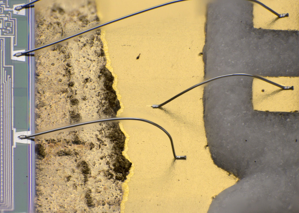
At the bondpad in the lower right corner there is a cutted wire. Whether this was done intentionally or the line was damaged during production cannot be said with certainty.


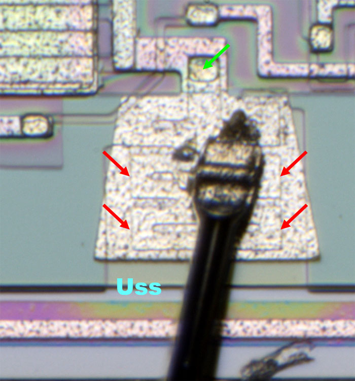
Underneath the bondpads you can spot a protective structure (red), which is contacted at the upper end of the bondpad (green). The whole structure represents a MOSFET with a thick gate oxide. When a problematic voltage pulse occurs, the structure becomes conductive, connecting the bondpad to the Uss potential and thus draining the pulse.


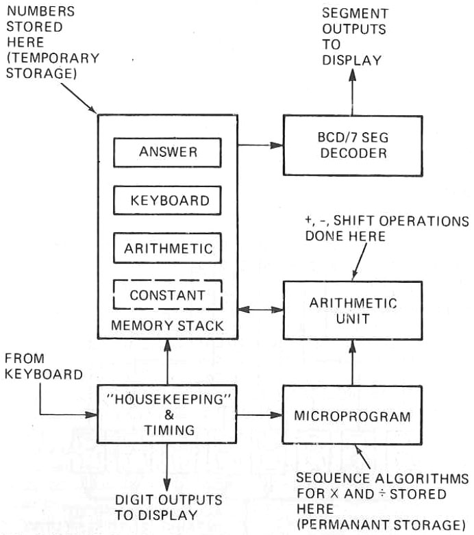
In the magazine "Radio Electronics" July 1974 there is a block diagram showing how a pocket calculator of this generation is constructed. The core of the microcontroller is the ALU which can perform addition, subtraction and shift operations. More complex calculations such as multiplications and divisions must be broken down to these operations.

A ROM contains the code necessary to control the system. A RAM provides the memory necessary to store the currently entered numbers, a constant, an intermediate result, and the end result.

The data is output via a BCD/7-segment decoder.


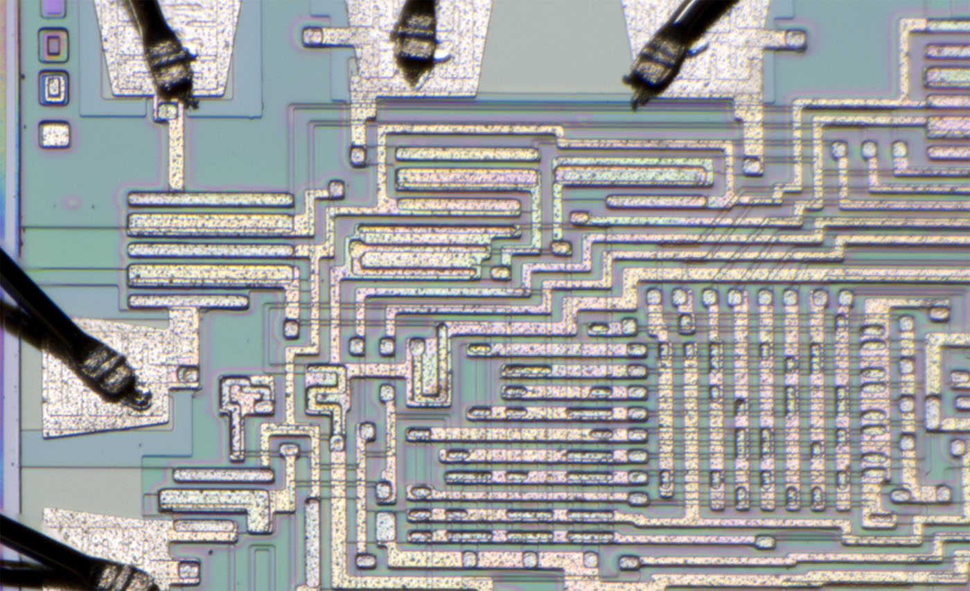
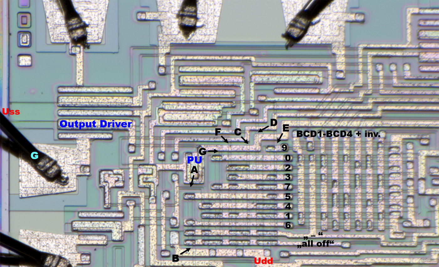
One part of the circuit that can be analyzed very well is the BCD/7-segment decoder. It consists of two blocks. The right block is differentially fed with the four BCD signals. In the matrix the distribution of the gate oxide areas ensures that one of the horizontally running lines becomes active depending on the BCD signals. Each line represents a number.

In the left block, the gate oxide areas are distributed in the horizontally running conductors in such a way that each of the numbers activates the appropriate segments of the display (A-G).

Each segment control line is connected to a pull-up structure and to a output driver. Some drivers are connected to Uss by connecting the frame structure.


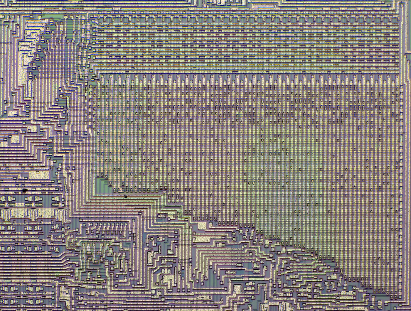
In the upper right area of the die is the ROM, which contains the control logic and takes up a lot of area. It is noticeable that the memory is not a square.

The upper area contains the column selection, which activates one out of 72 columns. On the side the rows output the necessary control signals. The upper rows seem to be partially coupled back to the column selection.


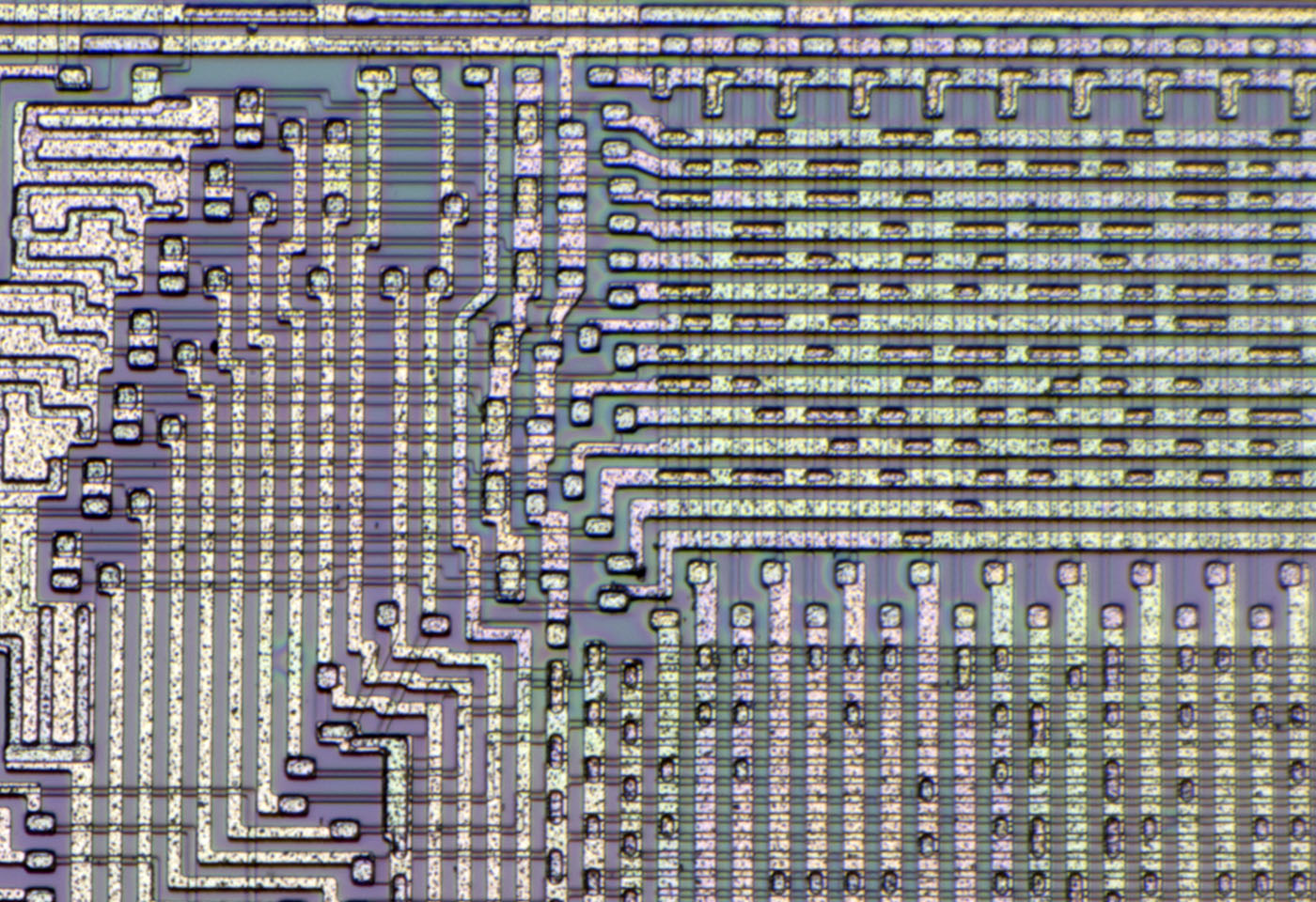
The distribution of the gate oxide areas represents the programm logic.


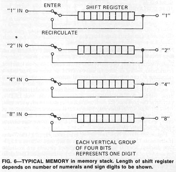
The already mentioned magazine "Radio Electronics" July 1974 shows the typical structure of the RAM in such a calculator. According to this, there are usually four shift registers which hold the four BCD signals. Each column in these four shift registers represents one digit. In addition, there are places for additional information such as sign and overflow.

The data passes through the shift registers continuously. This is necessary because it is usually DRAM that must be updated cyclically so that the information doesn´t degrade.


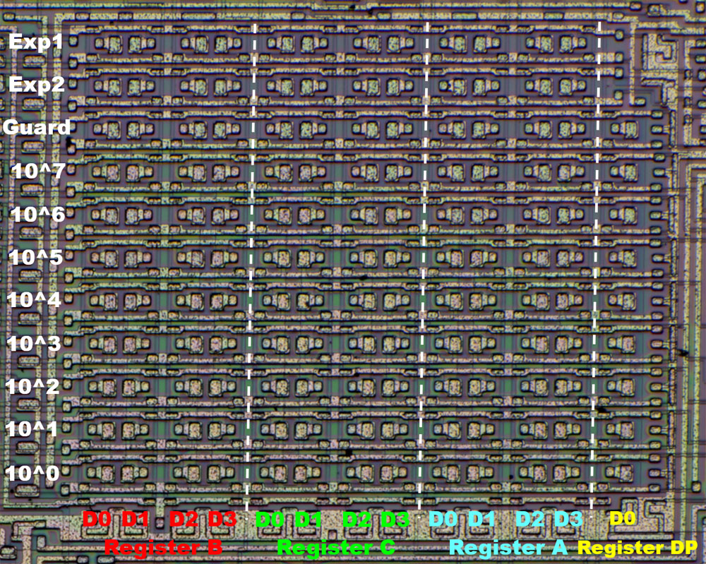
The RAM memory has 11 lines. In addition to the 8 digits of the display, there are consequently 2 bits left for sign and overflow. One bit must remain free so that the information can rotate in the shift register without additional intermediate memory.

The columns probably represent 3 groups of 4, representing 3 BCD numbers. We can assume that these are the memory areas for the current input, the subtotal and the result.

On the far right, there remains just one column with 9 individual memory cells. There the optional constant must be stored.  :-// The constant can only be used for multiplications and divisions. These operations are performed differently than additions and subtractions. Probably that is why they are stored as binary numbers. In addition, the possible number range does not have to be very large.


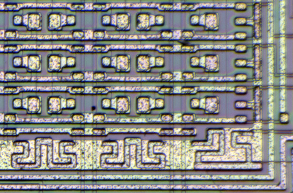
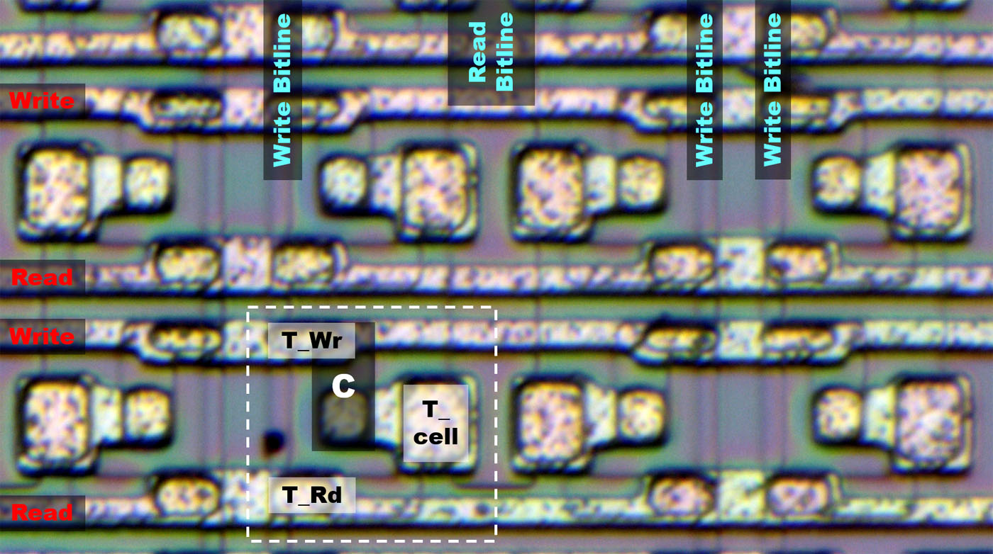
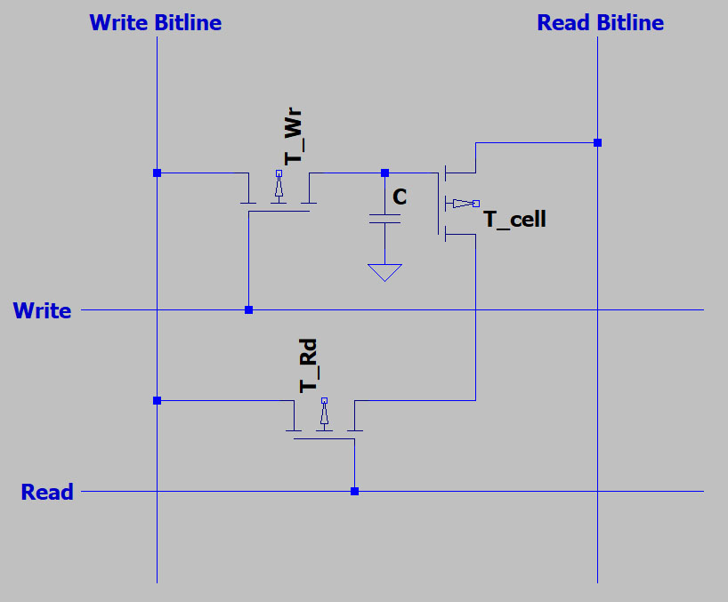
The individual memory cells are 3T1C cells, which are constructed with three transistors and a capacitor. The capacitor is just a slightly wider line in the silicon. It controls the transistor T_cell. In contrast to a 1T1C RAM like the U2164 (https://www.richis-lab.de/RAM02.htm), a 3T1C RAM has the advantage that a read operation does not erase the memory contents.

When configured as a shift register, the 3T1C configuration has another advantage. For the function as a memory it would be sufficient to connect the transistor T_Rd to Udd. Instead, the transistor is connected to the write bitline. Since the read out signal is low impediance in contrast to a 1T1C RAM, it can be fed directly into the next cell. Thus, one cycle is sufficient to transfer information from cell to cell.


https://www.richis-lab.de/calc02.htm

 :-/O
 
The following users thanked this post: Gyro, RoGeorge, capt bullshot

Offline NoopyTopic starter

  • Super Contributor
  • ***
  • Posts: 1729
  • Country: de
    • Richis-Lab
Re: Different die pictures
« Reply #211 on: June 05, 2022, 07:38:50 am »


The FX507A is a tone sequence decoder. It is used in radio systems and makes it possible to specifically address one or more receivers. For this purpose, the module outputs a configurable sequence of five tones and can itself respond to a 5-tone sequence. Different tones are standardized in different countries. The FX507 works with the ZVEI tones. The FX407 and FX607 offer CCIR and NATEL.

The manufacturer Consumer Microcircuits was founded in 1968 in the UK. The company still exists today.


The block diagrams in the datasheet show the working principle of the device. The FX507 needs a supply voltage between 10V and 15V, generates a bias with a voltage divider and an additional auxiliary voltage with a charge pump which has to be built up partly externally. The base clock is provided by a VCO, which puts out 156kHz.

The specific 5-tone sequence is configured by connecting the "DIGIT SEQUENCE OUTPUTS" (S1-S5) to the "DIGIT SELECT INPUTS". The outputs S1 to S5 represent the five digits which can be assigned with the tones 0 to 9. R repeats a tone. G is a placeholder to be able to address groups of different sizes.


The die is 4,6mm x 4,2mm.


In the upper left corner is the Consumer Microcircuits logo and the year 1983.


The abbreviation CML and the type designation FX507 can be found in the lower right corner. Next to it are five masks numbers. If K represents the revision of the masks, the design has been revised quite often. The structures on the right edge allow to evaluate the performance of the imaging process.

The bondpad of pin 1 on the far left of the image is marked with a 1.


A test structure is integrated at the upper edge of the die. This seems to be a transistor similar to the one in the CZL-550 (https://www.richis-lab.de/calc02.htm) which works with the substrate potential and accordingly gets by with two contacts. While the right area seems to represent a normal MOSFET, the left area could be an ESD protection transistor with a thick gate oxide at the same time.


Not all function blocks can be identified easily. However, the two ROM areas can be recognized very well.


https://www.richis-lab.de/FX507.htm

 :-/O
 
The following users thanked this post: SeanB, RoGeorge

Offline NoopyTopic starter

  • Super Contributor
  • ***
  • Posts: 1729
  • Country: de
    • Richis-Lab
Re: Different die pictures
« Reply #212 on: June 18, 2022, 07:05:14 pm »


The ULN2111 is an FM detector and limiter produced by Sprague. Many manufacturers had a similar device on offer: ECG 708, Motorola MC1357, National Semiconductor LM2111N, Signetics N5111A, Signetics ULN2111A, SGS TAA661, Tesla MAA661, Texas Instruments SN76643N.


The ULN2111 datasheet shown in the 1982 Sprague Integrated Circuits Data Book shows the integrated function blocks.


The Signetics datasheet shows the function a little simpler. Signetics apparently sold the device under two designations: N5111A and ULN2111A. There was a close cooperation between Sprague and Signetics. Sometimes even components of the other company were sold. It is quite possible that Signetics switched to the Sprague component.

At the input of the ULN2111A there is an amplifier stage, which ensures that a level of 400µV is enough for full scale drive. The term limiter comes from the fact that the gain is usually high enough to overdrive the input amplifier. The relevant modulation is preserved. However the following circuits are less disturbed by fluctuating input levels because the output of the input amplifier is almost always fully driven. The demodulator consists of an analog multiplier. An externally network has to be added that generates a 90° phase-shifted signal. This signal is multiplied by the original signal. The result is an output voltage that depends on the phase shift of the two signals. The actual phase shift deviates from the set 90° due to the FM modulation. This results in the demodulated signal at the output, which just needs a lowpass filter.


The Sprague Integrated Circuits Data Book 1982 contains a detailed schematic of the ULN2111, which has been colored for a better understanding. A diode chain generates two voltages which are used to set the bias (light blue). The higher voltage is buffered by two transistors. It supplies the input amplifiers and serves as a bias for the upper part of the analog multiplier. The second voltage is the bias voltage for the input amplifiers and the lower part of the analog multiplier.

The input amplifier consists of three differential amplifier stages. The output of each stage is buffered with an emitter follower. The first amplifier stage (pink) operates with a global feedback. The inverting inputs of the second and third amplifier stages (cyan) are connected to the bias voltage. The emitter follower of the third differential amplifier represents the output stage (dark green). Different levels can be tapped through two pins. The input amplifier offers a typical gain of 53dB.

One output of the input amplifier is internally fed directly to the analog multiplier. The network to be externally added uses one of the outputs and generates a 90° phase shifted signal. The phase-shifted signal passes through another emitter follower (yellow) before being fed to the analog multiplier.

The analog multiplier (red) has a current sink with its own reference potential (dark blue). The lower differential amplifier directly processes the output signal of the input amplifier. The upper differential amplifiers receive the phase-shifted signal from the buffer amplifier. The diode chain delivers the bias.

The output signal is delivered by an emitter follower (light green). A capacitor must be connected to the base potential through pin 14 which generates a low pass filter.

The ULN2111 contains some universally applicable circuits with a lot of contacts. For this reason it is also well suited to built different circuits.


The edge length of the die is 1.6mm. There are some not contacted elements and the number 11 in the upper left corner. Probably several devices were realized with this die by changing just the mask for the metal layer. 11 could stand for ULN2111. The ULN2136 is more or less the same device, but has an additional crude 7.8V voltage regulator and thus can be supplied with up to 20V. The not included circuit parts could be sufficient to represent a simple voltage regulator.


The Sprague Integrated Circuits Data Book 1982 shows the metal layer of the ULN2111. It does not match the design of the ULN2111 we have here. One can only assume that the circuit was fundamentally revised over time. After 12 years this is quite possible.


https://www.richis-lab.de/radio01.htm

 :-/O
 
The following users thanked this post: SeanB, RoGeorge

Offline NoopyTopic starter

  • Super Contributor
  • ***
  • Posts: 1729
  • Country: de
    • Richis-Lab
Re: Different die pictures
« Reply #213 on: June 20, 2022, 03:29:15 am »
No semiconductor today, just some words about how www.richis-lab.de developed over the years and about the purpose of the website:


2001
The development of a teslacoil can be followed via the address www.teslaspule.here.de.

2008
The website is extended with various electronic projects. For the time being this section has no own domain and can only be reached via www.home.vr-web.de/kaussler/lab.

2010
The domain www.richis-lab.de is registered.

2016 / 2017
The first pictures of integrated circuits are created.

2019
The website gets a responsive design, so that it is better displayed on smartphones.

2022
Every day an average of 400 visitors call up www.richis-lab.de. There are now more than 600 pages online with more than 6.500 images. The update rate is 3 articles per week.


The website is intended to help beginners in the field of electronics to understand the structure and operation of various integrated circuits. At the same time, it should enable experts to better understand specific properties of components.
Different types of counterfeits are documented and components are analyzed, which come from different manufacturers but are supposed to represent the same functions. Documentation of defective components allows to interpret failure mechanisms. Finally, some analyses make it possible to verify or disprove historical relationships.

No profit is made with this website. The income covers just a part of the expenses. I accept donations of parts as well as requests for analyses but the queue is very long. Parts with an interesting background story can be preferred though.

The website contains just simple HTML code and should display well on most devices. No cookies are used. Incorrect links, spelling mistakes and misrepresentations are welcome to be reported.


https://www.richis-lab.de/background.htm

 :-/O
 
The following users thanked this post: SeanB, brabus

Online magic

  • Super Contributor
  • ***
  • Posts: 6758
  • Country: pl
Re: Different die pictures
« Reply #214 on: June 20, 2022, 06:21:08 am »
The input amplifier consists of three differential amplifier stages. The output of each stage is buffered with an emitter follower. The first amplifier stage (pink) operates with a global feedback.
It looks like feedback just causes the DC level at the inverting input of the first stage to follow the noninverting input and you are supposed to place 100nF to ground at I-F DECOUPLE to filter out the RF signal from there.
 
The following users thanked this post: Noopy

Offline NoopyTopic starter

  • Super Contributor
  • ***
  • Posts: 1729
  • Country: de
    • Richis-Lab
Re: Different die pictures
« Reply #215 on: June 20, 2022, 06:28:41 am »
I agree with you. It's a special kind of feedback.  :-+

Offline NoopyTopic starter

  • Super Contributor
  • ***
  • Posts: 1729
  • Country: de
    • Richis-Lab
Re: Different die pictures
« Reply #216 on: July 21, 2022, 05:58:52 pm »
I have an update for the CZL-550 calculator!


Besides some minor corrections i have a better analysis of the ROM.

The upper area of the ROM contains the column selector which activates one of the 72 columns with seven differential control signals. Each column represents a command that activates some control lines that are led out of the ROM to the left.

There are two different addresses in the top 14 lines of the ROM. One of the addresses is fed back to the column selection where it activates the next command.

Below the addresses there is a control command and a test command in each of the columns. The result of the test defines which of the two addresses of the column is used for the next step. This address is selected directly to the left of the address memory area.

The leftmost commands have just 13 control signals available in addition to the two addresses. On the far right a command can be linked to any of the total 49 control lines.


With the pictures of the C550 Dunkelwind aka bITmASTER was able to extract the firmware and create a list of the commands. From his analysis also comes the knowledge that the ROM columns also contain test commands in addition to the control commands.

You can find the pdf with the firmware here:
https://www.richis-lab.de/images/calc/C550/C550Firmware.pdf


The RAM consists of thirteen columns. Three times four columns represent the three registers A, B and C. These are the intermediate memories for input, the subtotal and the result. Four memory cells each represent a BCD number. For the 8 digits with which the calculator calculates there are correspondingly eight lines in the RAM. The guard cells signal an overflow. The uppermost two lines contain the exponent.

The smaller register DP is used for several functions. It serves as a counter for multiplications, but it also serves as a memory for the location of the decimal point.


Based on the images of the C550 Dunkelwind (aka bITmASTER) was able to program an emulator.

You can find the emulator here:
https://www.richis-lab.de/images/calc/C550/Picolator.html


https://www.richis-lab.de/calc02.htm

 :-/O
 
The following users thanked this post: SeanB, brabus, RoGeorge

Offline NoopyTopic starter

  • Super Contributor
  • ***
  • Posts: 1729
  • Country: de
    • Richis-Lab
Re: Different die pictures
« Reply #217 on: July 29, 2022, 06:12:00 pm »


The SHT21 (right) is a humidity and temperature sensor developed by Sensirion. The edge length of the DFN housing is just 3mm. The humidity is resolved with 12Bit, the temperature with 14Bit. The device outputs data via I2C. The current consumption is just 300µA (@3V).

Even at very high quantities the SHT21 costs more than 6€. At the same time plug-in boards that are supposed to contain the STH21 are offered for less money. The component on the left and in the center of the picture is desoldered from such a board. If a protective layer is glued on the component as it was the case here, the obvious difference of the sensor is not visible. The sensor attracted attention because of its relatively large measuring error.


The housing shows a Pin1 marking and the letters AEKT which, however, cannot be assigned to any sensor or manufacturer.


The cutout in the housing has a diameter of 0,9mm on the plane of the die.


With 2,1mm x 1,2mm the die of the device takes up a large part of the package. Around the round active area a solid metal layer protects the underlying circuits from ambient light. Light could lead to unwanted current flows in the silicon.

The die has some free bond pads. It is quite possible that these contacts were used for tuning during manufacturing.


According to the datasheet the SHT21 determines the humidity via a change in capacitance. Usually, the capacitance of a plate capacitor is monitored, which contains a material that absorbs the air humidity and changes its permittivity in relation.

The sensing element of the present component consists of two semicircles constructed with interlocking electrodes. The construction is rather reminiscent of a resistive humidity sensor. The principle according to which the sensor works cannot be clearly explained optically.


In the lower left corner of the die there are shown some masks.


In the other corners of the die you can just about make out some designations but they do not allow to draw a definite conclusion about the manufacturer or model.

There could be the string Silabs in the lower right corner. Silabs manufactures resistive humidity sensors. Si7010 in the upper left corner would match. It would be a typical Silabs nomenclature. On the other hand, there is no Si7010.


https://www.richis-lab.de/thd01.htm

 :-/O
 
The following users thanked this post: SeanB, RoGeorge, capt bullshot

Offline NoopyTopic starter

  • Super Contributor
  • ***
  • Posts: 1729
  • Country: de
    • Richis-Lab
Re: Different die pictures
« Reply #218 on: July 29, 2022, 06:53:18 pm »
Small Update:
The four letter marking of the package seems to be typical for SiliconLabs sensors.

Offline NoopyTopic starter

  • Super Contributor
  • ***
  • Posts: 1729
  • Country: de
    • Richis-Lab
Re: Different die pictures
« Reply #219 on: August 24, 2022, 04:26:20 am »


u-blox SARA-R410M LTE-Modem

I´m too lazy to hotlink 68 pictures.  ^-^
Please click on the link, use your favoured translater or just enjoy the pictures:

https://www.richis-lab.de/modem01.htm

 :-/O

PS: There are nearly 2.500 pictures in the background consuming 92GB.  :o
« Last Edit: August 24, 2022, 04:28:15 am by Noopy »
 
The following users thanked this post: SeanB, capt bullshot, ch_scr, MegaVolt

Offline Cerebus

  • Super Contributor
  • ***
  • Posts: 10576
  • Country: gb
Re: Different die pictures
« Reply #220 on: August 24, 2022, 01:45:15 pm »
I´m too lazy to hotlink 68 pictures.  ^-^
Please click on the link, use your favoured translater or just enjoy the pictures:

I'm not adverse to that actually. I love this thread, however I'll often put off reading it for several days after it pops up in my unread messages simply because of the time it takes a page to re-cache all the pictures and render, doing a little dance as the pictures push the page around.

I do get why you post all the stuff here, and I'm appreciative of not having to keep a separate eye on your website. Have you ever considered posting or linking just very small thumbnails here with a click to expand/open on them? It would considerably improve page opening times but the effect wouldn't really take effect until the next rollover of a forum page (20 messages for most people I think).

Just food for thought.
Anybody got a syringe I can use to squeeze the magic smoke back into this?
 

Offline NoopyTopic starter

  • Super Contributor
  • ***
  • Posts: 1729
  • Country: de
    • Richis-Lab
Re: Different die pictures
« Reply #221 on: August 24, 2022, 03:04:50 pm »
I see your point and I agree with you that often there are too much pictures on one page

The best solution would be generating an english version of every page on my website. In fact that would be the same as I post here.
Nevertheless I would not be happy with just some pages having both languages and would have to update a huge amount of pages.  :(

Generating Thumbnails with that amount of pictures would consume quite some time too.

A "teaser" tag would help, so you have to click to unfold the content but this forum doesn't support such "teaser" tags.

It would be interesting to know how much people need the whole story here. Would it be enough to post that there is some news with a teaser picture and people read my website with the translating tool they like? These tools are quite good today. I even understand some russian sites.
It would still be possible to discuss whatever we want in here.

Offline Cerebus

  • Super Contributor
  • ***
  • Posts: 10576
  • Country: gb
Re: Different die pictures
« Reply #222 on: August 24, 2022, 03:32:56 pm »
Generating Thumbnails with that amount of pictures would consume quite some time too.

That's pretty easy with command line tools. You can leave the computer to rip its way through a particular directory, or filenames that match a particular pattern, and go off and get on with your day leaving it to do its thing. Easy enough to find instructions for that on the Intardnet so i won't clutter here with a description of how to do it.
Anybody got a syringe I can use to squeeze the magic smoke back into this?
 

Offline NoopyTopic starter

  • Super Contributor
  • ***
  • Posts: 1729
  • Country: de
    • Richis-Lab
Re: Different die pictures
« Reply #223 on: August 24, 2022, 04:11:13 pm »
My text was a little mistakable.

Generating the thumbnails would be no bigger problem bit it would consume considerable more time to post them here:

Today I open the new site at richis-lab.de, copy the link of the picture, post it here in the img-Tag, copy the text, translate it with deepl, do a quick check of the text and done.

With the thumbnails I would have to change the picture link to get the thumbnail and put a link around it to the big picture.
That sound not like a huge amount of additional effort but you have to consider how much pictures I upload. That accumulates quite some time.


And I have to say I for myself don't like it when I have to click on every picture to see what is going on.
That is one thing I like at xdevs.com https://xdevs.com/article/hpak66xx/
A lot of nice high resolution pictures.  8)

Offline Amper

  • Frequent Contributor
  • **
  • Posts: 286
  • Country: 00
Re: Different die pictures
« Reply #224 on: August 26, 2022, 02:24:30 pm »
Hi!

I just took some images of a DRV8302 with the keyence microscope because i was puzzled why i could just not see anything under my sem.
Really interesting Ti seems to do this not only on high end stuff but ob sort of regular components.

The passivation under the masking layer seems to be something like 5-10um, maybe it can be polished off.


Share me

Digg  Facebook  SlashDot  Delicious  Technorati  Twitter  Google  Yahoo
Smf