Author Topic: ifi iPower teardown  (Read 2724 times)

0 Members and 1 Guest are viewing this topic.

Offline HawakaTopic starter

  • Regular Contributor
  • *
  • Posts: 97
  • Country: ch
ifi iPower teardown
« on: February 15, 2024, 09:58:15 pm »
At ~70USD the ifi iPower is certainly expensive for a +5V 2.5A power supply, but does it deliver the ultra-quiet, ultra-clean audiophile-grade power it claims?

Short answer: Yes, probably.

Long answer: See below.

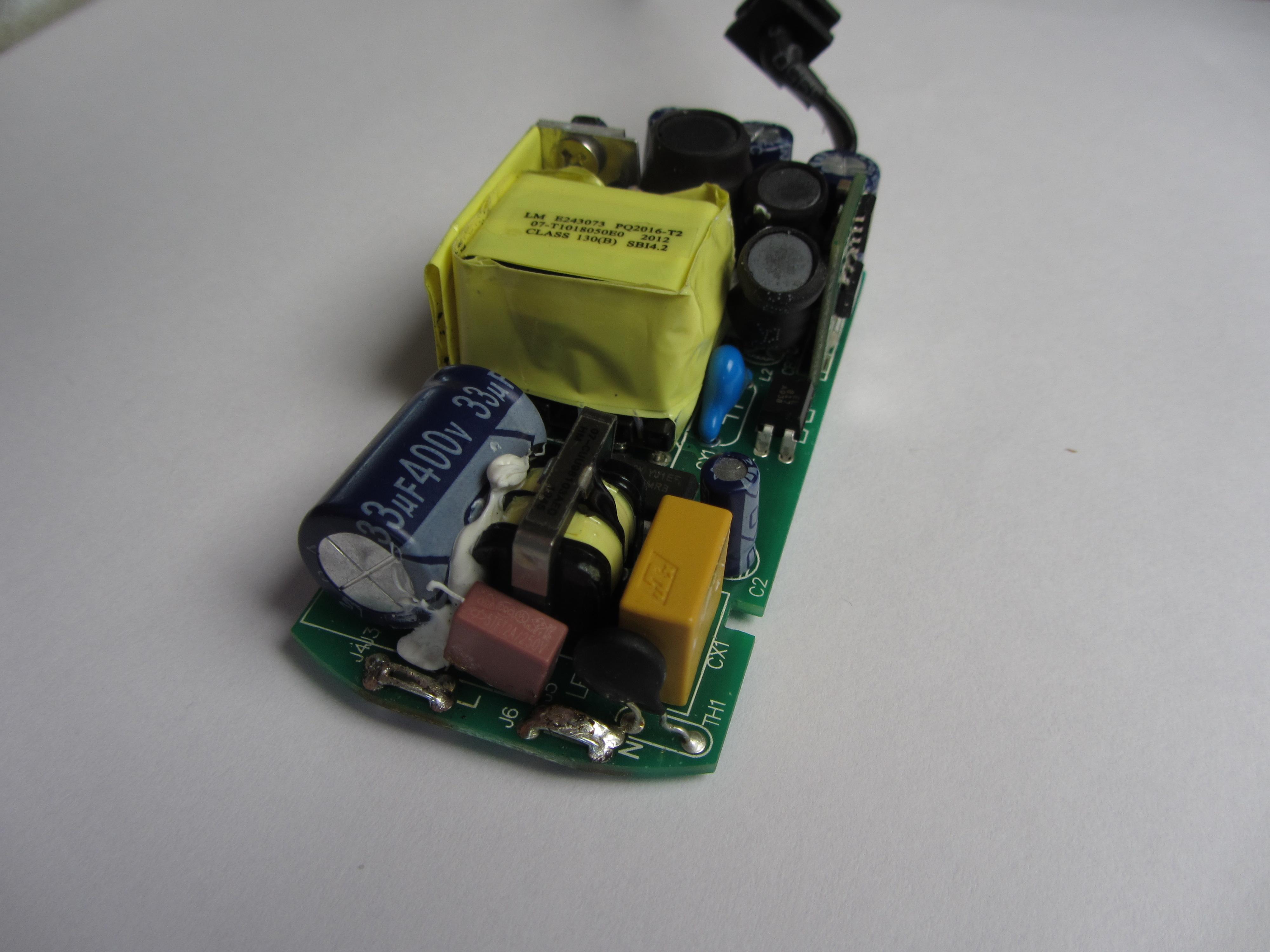
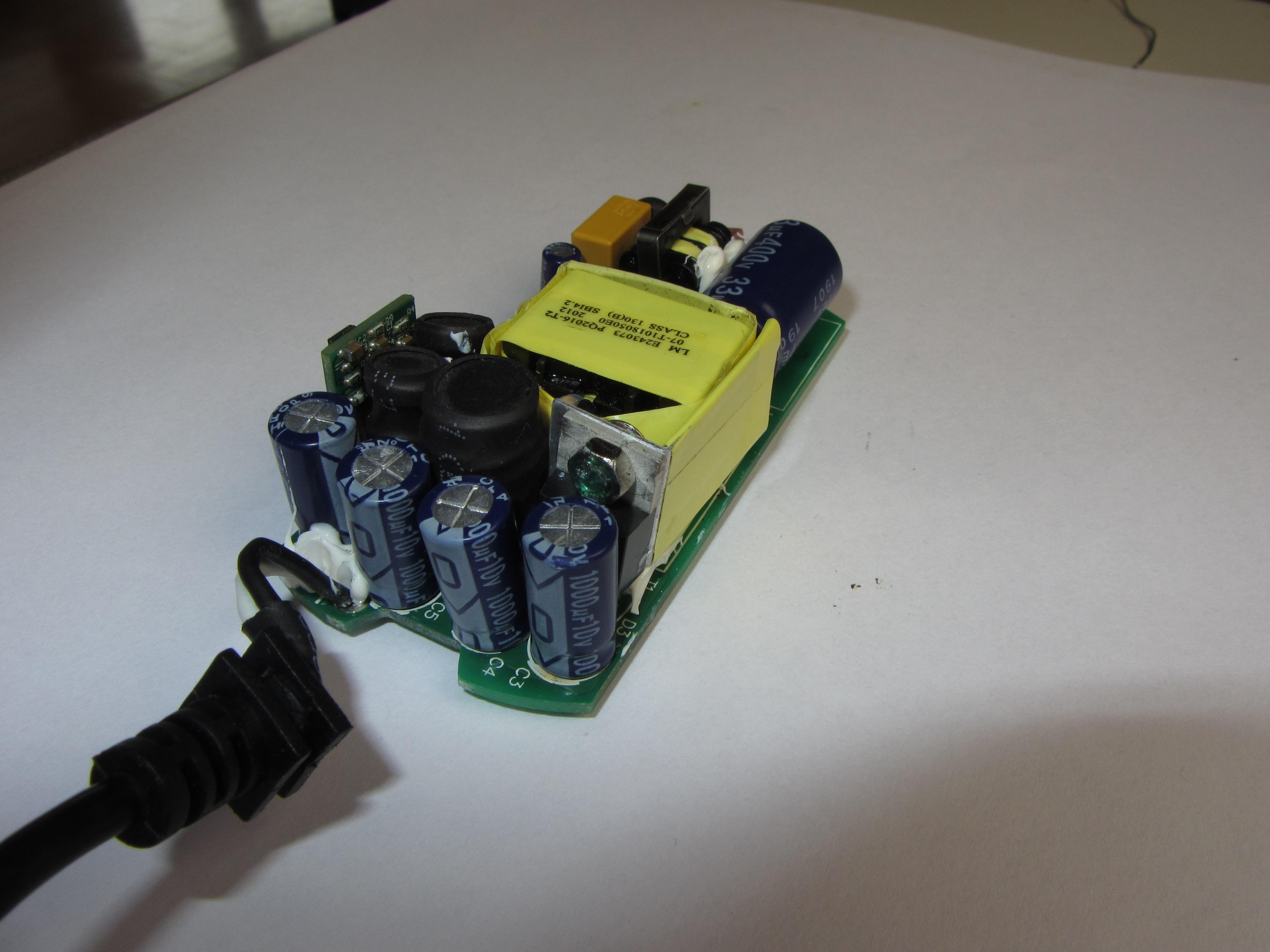
The iPower does deliver a supply with significantly less noise than others, and it does so out of the box. It is on the expensive side (or not for audiophile-grade device), but at least you are sure you won't hear a humming sound once plugged into your system (or your test/measuring equipement). It comes in the box with a fairly wide choice of wall adaptor and jack adaptor. Build quality is standard.
2019005-02019011-1

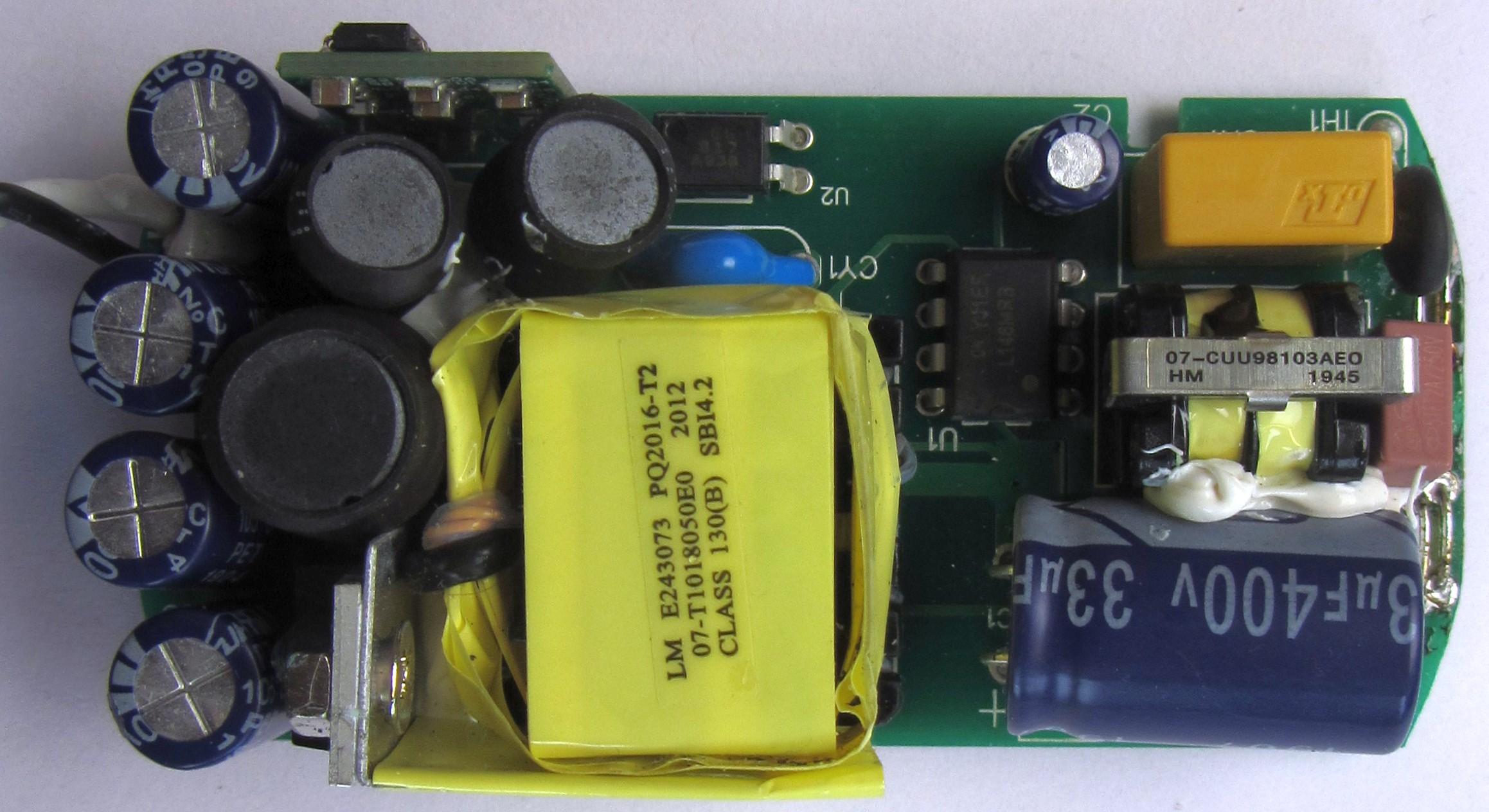
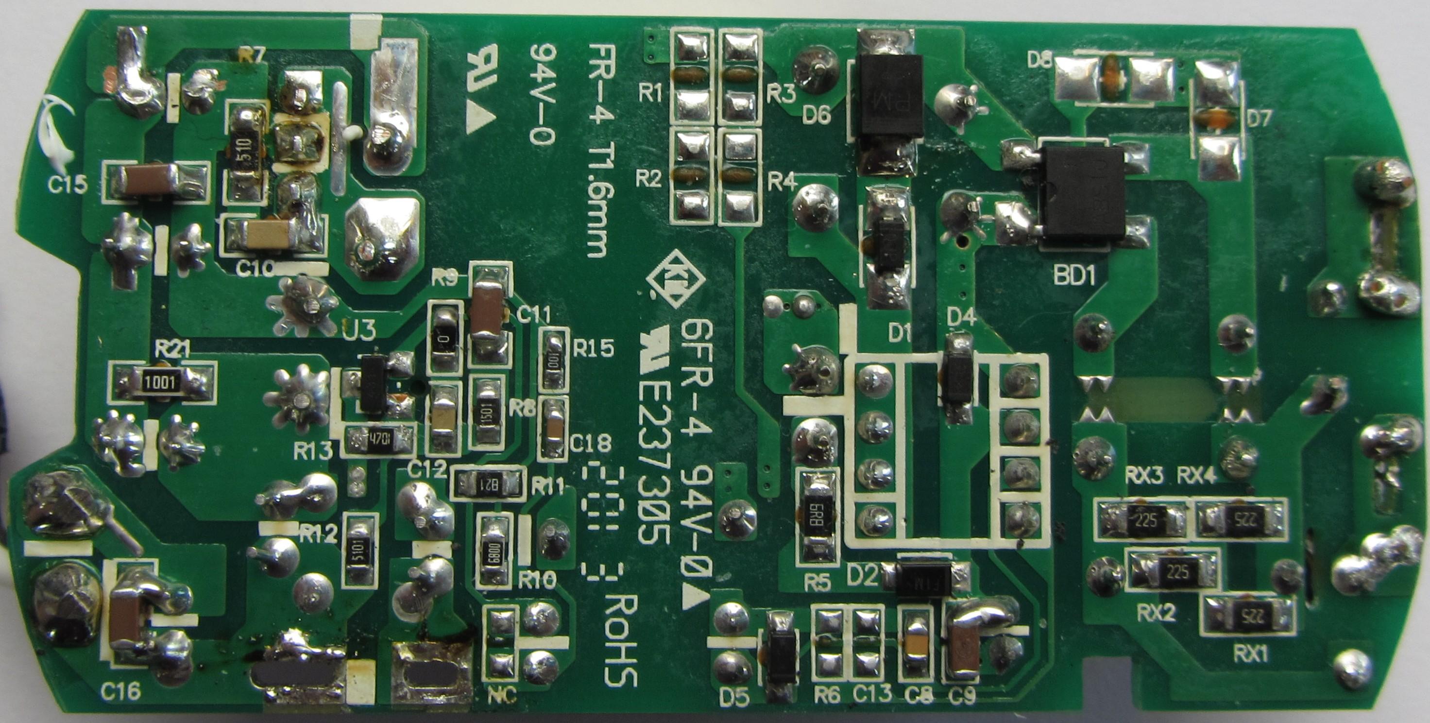
The supply has 2 PCBs, 1 main board and an additionnal board in parallel of the output. The main board is a flyback converter with a TL431 as reference. The second board has a BJT with an IC that I cannot recognised, marked "OV 1028" (no brand).
2019017-22019023-3
2019029-4


The circuit with the TL431 and the diode side of the optocoupler is quit strange.

2019035-5


The second PCB, with a ZT2907A BJT has most certainly something to do with noise-cancelling. The IC marked "OV 1028" is a mystery. An LT1028 could be a fit, but I don't understand pin 1, 8 and the negative feedback looks strange to me. Pin 8 is unconnected on the schema, as I couldn't find where it goes.

Following is a noise comparaison against a few USB +5V supply. A resistive load is used, measurements BW is 10Hz to 100kHz. The iPower has a very low noise, but it is hard to tell if the claimed noise floor of 1uV is reached.

2019041-6


IMO this power supply is pretty good, and at least for an audiophile product it tries to do what it claims. Still expensive, but if you have to test 5 differents supply before finding the one that has a low enough noise floor, you'll probably save money and time by buying this one.
 
The following users thanked this post: D Straney, 5U4GB

Offline HawakaTopic starter

  • Regular Contributor
  • *
  • Posts: 97
  • Country: ch
Re: ifi iPower teardown
« Reply #1 on: February 15, 2024, 10:01:21 pm »
Here is the schematic an the KiCad file.
 

Offline D Straney

  • Regular Contributor
  • *
  • Posts: 189
  • Country: us
Re: ifi iPower teardown
« Reply #2 on: February 17, 2024, 09:57:03 pm »
Nice look inside.  I think the pinout's flipped on the TL431, which is why the circuit looks so weird: swap the cathode and ref pin, and it'll make a lot more sense.  There are different variants of these with different pinouts that I've run across (probably to make cheap single-sided power supply layouts easier).

With that pin swap, now it has a voltage divider from Vout feeding the reference pin: 51KΩ high-side, 4.7KΩ low-side.  C12 bridges the cathode and ref, providing local negative feedback integrator-style.  R8 and C11 provide an "alternate" high-side for the voltage divider, AC-only, to remove the phase lag of the output EMI filter from the control loop (otherwise the LC filters add a whole of phase lag to the loop response, and makes you cut your control loop bandwidth WAY down to remain stable).  Taking the DC output from after the EMI filter allows it still regulate the steady-state level properly to account for voltage drops in the series inductors.

Offline huababua

  • Contributor
  • Posts: 19
  • Country: de
Re: ifi iPower teardown
« Reply #3 on: March 29, 2024, 06:18:47 pm »
Did you get any further with the second "noise canceling" pcb?
 

Offline HawakaTopic starter

  • Regular Contributor
  • *
  • Posts: 97
  • Country: ch
Re: ifi iPower teardown
« Reply #4 on: March 29, 2024, 09:48:14 pm »
Not really. If I could identify the IC marked "OV 1028" that would really help, but so far no luck. The LT1028 is also weird, with pin 1 and 8 for the same function. On the PCB these two pins are not connected together with a full short (if I remember correctly something around 800R between the pins).
 

Offline 5U4GB

  • Frequent Contributor
  • **
  • Posts: 391
  • Country: au
Re: ifi iPower teardown
« Reply #5 on: March 30, 2024, 11:14:42 am »
for an audiophile product it tries to do what it claims.

An audiophile product that isn't just woo-woo?  Perhaps it should be put on display somewhere to prove that such a thing exists :-).

Did you read their tech note on how they measured the noise figures to get the uV claim?
 

Offline HawakaTopic starter

  • Regular Contributor
  • *
  • Posts: 97
  • Country: ch
Re: ifi iPower teardown
« Reply #6 on: March 30, 2024, 11:38:00 am »
Yeah I did, pretty funny technical document for a serious company ;)

Noise measurement is hard in any case, so I just went the way I could without expecting too much.
 
The following users thanked this post: 5U4GB

Offline NiHaoMike

  • Super Contributor
  • ***
  • Posts: 9021
  • Country: us
  • "Don't turn it on - Take it apart!"
    • Facebook Page
Re: ifi iPower teardown
« Reply #7 on: March 30, 2024, 12:15:46 pm »
I'm surprised they didn't split the Y capacitor into 2 in series with the midpoint connected to ground, that would substantially reduce the common mode noise.
Cryptocurrency has taught me to love math and at the same time be baffled by it.

Cryptocurrency lesson 0: Altcoins and Bitcoin are not the same thing.
 

Offline huababua

  • Contributor
  • Posts: 19
  • Country: de
Re: ifi iPower teardown
« Reply #8 on: March 31, 2024, 01:55:12 pm »
Not really. If I could identify the IC marked "OV 1028" that would really help, but so far no luck. The LT1028 is also weird, with pin 1 and 8 for the same function. On the PCB these two pins are not connected together with a full short (if I remember correctly something around 800R between the pins).

I found the part number on an old www.rf-china.com side.

Anyway - I think it must be an opamp.

The base principle should be something compared to existing circuits for „active EMI filter“.
Here is one example with a more complex implementation using an extra winding in a transformer:

http://dspace.mit.edu/bitstream/handle/1721.1/87314/51972993-MIT.pdf;sequence=2

Do you think this circuit is floating on the output voltage of the SMPS or is it generating it own reference with the led?
 
The following users thanked this post: 5U4GB

Offline HawakaTopic starter

  • Regular Contributor
  • *
  • Posts: 97
  • Country: ch
Re: ifi iPower teardown
« Reply #9 on: March 31, 2024, 03:02:27 pm »
I really have no idea how the second PCB works. The concept of having a BJT that can short-circuit the output, but somehow reduce the voltage noise escape me. If it was to reduce current variation by keeping a constant load on the transformer it would make more sense, but that is clearly not what is happening here.
« Last Edit: March 31, 2024, 04:22:16 pm by Hawaka »
 

Offline coromonadalix

  • Super Contributor
  • ***
  • Posts: 5906
  • Country: ca
Re: ifi iPower teardown
« Reply #10 on: March 31, 2024, 03:59:59 pm »
seems pretty basic  with more filtering on the output

you want to see if it's noisy,  load it with a 2.5 amp, say resistive load and check with an isolated scope the noise it gives on the output

medical grade psu are more "silent" than normal ones

and some smps  psu's   can have higher frequencies switching to get noise lower or harmonic beyond audio usages

i've seen up to 300khz and 600khz, even a 1 meg Hz once in my life,   not expensive and keep the noise out  ??
« Last Edit: March 31, 2024, 04:07:21 pm by coromonadalix »
 

Offline D Straney

  • Regular Contributor
  • *
  • Posts: 189
  • Country: us
Re: ifi iPower teardown
« Reply #11 on: March 31, 2024, 10:53:56 pm »
I really have no idea how the second PCB works. The concept of having a BJT that can short-circuit the output, but somehow reduce the voltage noise escape me. If it was to reduce current variation by keeping a constant load on the transformer it would make more sense, but that is clearly not what is happening here.

Yeah, it's a little unintuitive, as it would make no sense at DC (as the output impedance of the supply is very very low at DC so it would just burn power for no reason).  I thought it was acting against the AC output impedance of the power supply's output filter, which is significant at higher frequencies, but still seems possibly too large to be practical, so I might be missing something?

Let's look at 100 kHz, for example: if the inductors are something like 10µH then their impedance will be +j6Ω, and the 1000µF cap will be -j1.6mΩ (which means that in practice its impedance will bottom out at its ESR, so something like 0.5Ω ballpark); so overall the cap's ESR dominates as far as source impedance.  So if you're trying to suppress a 10 mV pk ripple, then you need to draw 10 mV/0.5Ω = 20 mA pk.  Then to do the negative swing as well you need to go full class-A and have a 20 mA steady-state current draw (100 mW) so that you can reduce it by 20 mA as well as increasing it.  This isn't so bad at 100 kHz+, but the current consumption gets worse as you go down in frequency so I'm not sure how low this active suppression is supposed to work.  I think the range over which it's practical really depends on the output cap ESR, and those final filter inductor values.

Offline huababua

  • Contributor
  • Posts: 19
  • Country: de
Re: ifi iPower teardown
« Reply #12 on: April 01, 2024, 09:40:12 am »

Let's look at 100 kHz, for example: if the inductors are something like 10µH then their impedance will be +j6Ω, and the 1000µF cap will be -j1.6mΩ (which means that in practice its impedance will bottom out at its ESR, so something like 0.5Ω ballpark); so overall the cap's ESR dominates as far as source impedance.  So if you're trying to suppress a 10 mV pk ripple, then you need to draw 10 mV/0.5Ω = 20 mA pk.  Then to do the negative swing as well you need to go full class-A and have a 20 mA steady-state current draw (100 mW) so that you can reduce it by 20 mA as well as increasing it.  This isn't so bad at 100 kHz+, but the current consumption gets worse as you go down in frequency so I'm not sure how low this active suppression is supposed to work.  I think the range over which it's practical really depends on the output cap ESR, and those final filter inductor values.


As this is a SMPS there should be no huge noise in the lower frequ. region. Also - the pcb itself works without heatsink which means there isnt too much heat dissipation.

From the pin numbers in Hawakas schematic it is almost clear that this must be kind of a opamp - with Pin 2 and 3 beeing the inputs, 7 and 4 are power and Pin 6 is output. These are standard pins for an opamp in an SO-8 package. Only pin what I cant figure out is Pin 1 with a small capacitor going to the collector. My first guess was this is some way of external compensation but having a single capacitor on a pin doesnt make any sense.
Maybe they fooling us :p any other ideas?


Edit: found some measurements for this SMPS: https://audiophilestyle.com/forums/topic/31119-power-supply-8-group-test-lps-and-smps/
« Last Edit: April 01, 2024, 09:42:01 am by huababua »
 

Offline D Straney

  • Regular Contributor
  • *
  • Posts: 189
  • Country: us
Re: ifi iPower teardown
« Reply #13 on: April 01, 2024, 02:27:56 pm »
You're right, of course - the worst noise would be concentrated in that fsw-and-harmonics range (100 kHz+) where that works well because the output inductors are nice and high-impedance. At light loads, bust-mode operation will create lower frequencies in the output but there's other ways around that.

I've seen some single op-amps with pins 1 and 8 used as offset trim, which means you have access to the collectors of the input diff pair from there. Could see the cap being a way to inject some negative feedback current for loop stability (the collector voltage is essentially a current sense voltage due to the 22 ohm resistor) - bit unconventional but makes sense.

Offline huababua

  • Contributor
  • Posts: 19
  • Country: de
Re: ifi iPower teardown
« Reply #14 on: April 01, 2024, 05:32:51 pm »
Completely agree with you on that point. From the measurements I have posted above you can see quite good where the filtering is doing its work compared to a “switching only” power supply.


So in that case pin 1 would be directly accessing the input transistor of the negative input and pin 8 the bjt of the positive?
I will try to get a spice simulation running in this.

Yeah… with all that wodoo about noise in acoustic applications I am not surprised to see some mystic implementations here.


Offline HawakaTopic starter

  • Regular Contributor
  • *
  • Posts: 97
  • Country: ch
Re: ifi iPower teardown
« Reply #15 on: April 02, 2024, 05:41:20 pm »
Let's not forget that this is an audio product, so the noise <100kHz (or even <40kHz) matters probably more than >100kHz.


Share me

Digg  Facebook  SlashDot  Delicious  Technorati  Twitter  Google  Yahoo
Smf