Author Topic: LM723 die pictures  (Read 27014 times)

0 Members and 1 Guest are viewing this topic.

Offline NoopyTopic starter

  • Super Contributor
  • ***
  • Posts: 1731
  • Country: de
    • Richis-Lab
LM723 die pictures
« on: January 21, 2020, 10:59:34 pm »

I decided to open a new thread. I hope that´s ok for everybody. In the 555-thread it would be to far off topic.


In the 555-die-thread Wolfgang asked for pictures of the LM723:
https://www.eevblog.com/forum/projects/some-555-timer-dies/msg2870226/#msg2870226

Done that:


Link to my site:
https://www.richis-lab.de/LM723.htm


I didn´t write very much about it because Wolfgang has already written a lot:
https://electronicprojectsforfun.wordpress.com/power-supplies/a-collection-of-proper-design-practices-using-the-lm723-ic-regulator/

What I realized looking at the die:
It seems that the design is the one you can find in the older datasheet. The schematic in the current datasheet is much more complicated.
I couldn´t figure out when this LM723 was produced but it didn´t look too old to me.
Perhaps I should decap one more LM723...  ::)


Greetings,


Richard

Offline wraper

  • Supporter
  • ****
  • Posts: 16853
  • Country: lv
Re: LM723 die pictures
« Reply #1 on: January 21, 2020, 11:36:33 pm »
It seems that the design is the one you can find in the older datasheet. The schematic in the current datasheet is much more complicated.
No wonder. On the photo on your website IC looks to be salvaged, sanded, blacktopped and marked again. Look on the tiny holes in ST logo.
 
The following users thanked this post: Wolfgang

Offline NoopyTopic starter

  • Super Contributor
  • ***
  • Posts: 1731
  • Country: de
    • Richis-Lab
Re: LM723 die pictures
« Reply #2 on: January 22, 2020, 04:29:17 am »
Hm, didn´t see that at once but probably you are right.  :-+
I think I have to dedcap one more...  ;D

Offline BravoV

  • Super Contributor
  • ***
  • Posts: 7547
  • Country: 00
  • +++ ATH1
Re: LM723 die pictures
« Reply #3 on: January 22, 2020, 04:48:56 am »


Have a bunch of these, given by my mentor many-many years ago.

PM me your address, once I get home (currently on travel), I will send you this TO-200 can type 723.

PS : I will be sending used one.
« Last Edit: January 22, 2020, 05:10:26 am by BravoV »
 
The following users thanked this post: Kartika

Offline NoopyTopic starter

  • Super Contributor
  • ***
  • Posts: 1731
  • Country: de
    • Richis-Lab
Re: LM723 die pictures
« Reply #4 on: January 22, 2020, 06:52:54 pm »
Hello BravoV,

thanks for your offer.  :-+
I will send you my adress.

Offline David Hess

  • Super Contributor
  • ***
  • Posts: 16611
  • Country: us
  • DavidH
Re: LM723 die pictures
« Reply #5 on: January 22, 2020, 07:11:04 pm »
It seems that the design is the one you can find in the older datasheet. The schematic in the current datasheet is much more complicated.

The published schematics are often considerably simplified like with the common 324/358 schematics although I understand that there is more than one version of the 723.
 

Offline NoopyTopic starter

  • Super Contributor
  • ***
  • Posts: 1731
  • Country: de
    • Richis-Lab
Re: LM723 die pictures
« Reply #6 on: January 22, 2020, 07:23:10 pm »
The published schematics are often considerably simplified like with the common 324/358 schematics although I understand that there is more than one version of the 723.

In this case the circuit on the die is simpler than the newer shematics.
There are definitely missing a lot of parts on "my" die.

I definitely need a new one…  :)

Offline magic

  • Super Contributor
  • ***
  • Posts: 6773
  • Country: pl
Re: LM723 die pictures
« Reply #7 on: January 22, 2020, 10:20:59 pm »
The "new" schematic may be a redesign by National.

Wolfgang's website has an old µa723 application note from Fairchild which shows a schematic very similar to your die.
An even more accurate match is the schematic from Motorola datasheet, but there are a few dumb and confusing errors. The circuit wouldn't ever work as drawn :palm:
Old TI datasheet (before National acquisition) also shows the same schematic as Motorola, without errors.

So there is quite a bit of agreement, and only National sticks out as the weird one. Some datasheets (ST, Philips) have no schematic at all.

And since Texas Instruments absolutely has no taste and looking at their schematics makes me want to throw up, I post corrected Motorola schematic below, which appears to match your die. Enjoy :)

edit
Added the Fairchild schematic for completeness. The only difference I can see is Q9 and Q11 collectors. I have no idea if the original Fairchild die matched the Fairchild schematic or maybe was like everybody else's.

I also don't understand what was the point of connecting Q9 and Q11 collectors to Q4 and Q5. VCC is available in the isolation well right underneath Q4 and Q5, they could have used that if they wanted to.
« Last Edit: January 22, 2020, 10:40:23 pm by magic »
 
The following users thanked this post: edavid

Online iMo

  • Super Contributor
  • ***
  • Posts: 4775
  • Country: pm
  • It's important to try new things..
Re: LM723 die pictures
« Reply #8 on: January 22, 2020, 10:27:55 pm »
FYI - TESLA's MAA723 (with 4 additional resistors) :)
PS: they did DIL14 and metal can
« Last Edit: January 22, 2020, 10:45:36 pm by imo »
 

Offline floobydust

  • Super Contributor
  • ***
  • Posts: 6972
  • Country: ca
Re: LM723 die pictures
« Reply #9 on: January 22, 2020, 11:10:17 pm »
The uA723 I believe was originally developed by Bob Widlar in 1967 not sure who developed it (it incorporates his current source). Oldest oldest data I can find is from Fairchild 1971 attached schematic.

Wikipedia: "Widlar's productivity was so great that it has stimulated spurious attributions. A prevalent example erroneously credits him with the design of the μA723 voltage regulator. However, not only was that chip released some two years after Widlar's departure from Fairchild, the circuit employs, and relies on, greatly improved lateral PNP transistors that were not available during the period of Widlar's employment at Fairchild. Credit for the μA723 properly belongs to Darryl Lieux, according to his contemporary (and father of the 741), Dave Fullagar. [48]'

National Semiconductor AN-1 (yes app note #1) November 1967 is all about the LM100 which is quite similar to the uA723 but likely got snarled in patent litigation. The voltage reference, foldback current-limiting all were patented blocks between National and Fairchild, which maybe why the LM100 didn't make it.

edit: 1973 databook here: https://archive.org/details/bitsavers_fairchilddldLinearIntegratedCircuitsDataCatalog_30443462
edit2: 1968 Fairchild uA723 App note http://www.ve6aqo.com/old_manuals.htm
« Last Edit: January 22, 2020, 11:23:42 pm by floobydust »
 

Offline NoopyTopic starter

  • Super Contributor
  • ***
  • Posts: 1731
  • Country: de
    • Richis-Lab
Re: LM723 die pictures
« Reply #10 on: January 23, 2020, 04:28:06 am »
Thanks for all your input!

I will have to collect some more of the LM723-variants.  ;D

Offline magic

  • Super Contributor
  • ***
  • Posts: 6773
  • Country: pl
Re: LM723 die pictures
« Reply #11 on: January 23, 2020, 09:00:22 am »
So a few remarks for Wolfgang, if you are reading this ;)

It wasn't exactly the legendary Widlar and, pending further research, the National schematic may not even be true to the original Fairchild design.

And I also doubt it's a buried zener. Looks like any other NPN BE junction visually and the Fairchild appnote (page 1.12) brags about a state of the art process capable of integrating even N-JFETs and capacitors in addition to NPNs and PNPs ;D
 

Online iMo

  • Super Contributor
  • ***
  • Posts: 4775
  • Country: pm
  • It's important to try new things..
Re: LM723 die pictures
« Reply #12 on: January 23, 2020, 09:04:44 am »
No buried zener in 723. And frankly, I doubt there is even a zener as the Vref.
The Vref is quite noisy, I saw 2mV p-p noise there, moreover, Wolfgang confirmed that in his measurements.
PS: I like the 723 (because I built my first PSU around it). On the other hand the stories about its "Vref stability and low noise" are just urban myths, imho.

« Last Edit: January 23, 2020, 09:51:48 am by imo »
 

Offline magic

  • Super Contributor
  • ***
  • Posts: 6773
  • Country: pl
Re: LM723 die pictures
« Reply #13 on: January 23, 2020, 09:10:49 am »
Of course there are two zeners: one for Vref and one for bias generation.

The bottom right pad is the buffered Vref output. Next one above is the GND pad. Between them is the 5pF compensation capacitor and two NPNs: Q6 on the right, and D2 on the left. The BE junction is used, just like for D1 elsewhere.
 

Online iMo

  • Super Contributor
  • ***
  • Posts: 4775
  • Country: pm
  • It's important to try new things..
Re: LM723 die pictures
« Reply #14 on: January 23, 2020, 09:23:30 am »
Is that a real zener or a reverse biased transistor junction?
 

Offline magic

  • Super Contributor
  • ***
  • Posts: 6773
  • Country: pl
Re: LM723 die pictures
« Reply #15 on: January 23, 2020, 09:33:43 am »
No idea. Looks like any other junction and they don't brag about any special technology in the appnote or datasheet so probably a fake zener, if reverse biased transistors aren't real zeners :)
 
The following users thanked this post: iMo

Offline floobydust

  • Super Contributor
  • ***
  • Posts: 6972
  • Country: ca
Re: LM723 die pictures
« Reply #16 on: January 24, 2020, 02:23:21 am »
Noopy, thanks for the archaeological digs.

I find it odd the uA723 won the wars. The 1968 Fairchild App note shows the LM100 schematic...  :-//
Most claims for better performance are due to better IC technology - compensation capacitors, lateral PNP's - but it might have been price or lack of military use that sank the LM105. Application Note 23 - The LM105- An Improved Positive Regulator Robert Widlar January 1969 explains the LM100 limitations, zener noise etc.
Many National Semi IC's came and went, in the 1970's, despite them being fine parts.

About the V reference design, it's mentioned in AN-1 the differences between using a reverse-biased EB junction and avalanche diode, for best tempco. A second goal is compatibility with the IC process so 'surface impurity concentrations' do not need to be specialized. I have a paper databook with AN-1 but could not find on the web.
 

Offline magic

  • Super Contributor
  • ***
  • Posts: 6773
  • Country: pl
Re: LM723 die pictures
« Reply #17 on: January 24, 2020, 08:44:04 am »
About the V reference design, it's mentioned in AN-1 the differences between using a reverse-biased EB junction and avalanche diode, for best tempco. A second goal is compatibility with the IC process so 'surface impurity concentrations' do not need to be specialized. I have a paper databook with AN-1 but could not find on the web.
Attached :)

It's included in National's 1973 Linear Applications book and you can find scans of that.

Typing "the first buried zener reference" into web search, I also found this book, which claims that this technology was introduced by the familiar LM199/399.
https://books.google.com/books?id=03JmxpE39N4C&pg=PA7&lpg=PA7&dq=the+first+buried+zener&source=bl&ots=5yhwN6_hv9&sig=ACfU3U0SGgYYnUaYj1lyauVYqAOng6TQHQ&hl=pl&sa=X&redir_esc=y

And back to
what was the point of connecting Q9 and Q11 collectors to Q4 and Q5.
I suppose it's for better power supply rejection. And a side effect is limitation of the regulation amplifier's common mode input range to a diode drop or two above Vref, which means that this tweak was likely not introduced by second sources but by Fairchild themselves. Apparently they concealed it in the documentation to protect their secret sauce :)
 
The following users thanked this post: iMo, Noopy

Offline BravoV

  • Super Contributor
  • ***
  • Posts: 7547
  • Country: 00
  • +++ ATH1
Re: LM723 die pictures
« Reply #18 on: January 30, 2020, 04:12:10 pm »
Two of these are on their way to Noopy.  :P

National Semiconductor LM723CH date code 8848, and Fairchild UA723HC date code 8335.

Offline NoopyTopic starter

  • Super Contributor
  • ***
  • Posts: 1731
  • Country: de
    • Richis-Lab
Re: LM723 die pictures
« Reply #19 on: January 30, 2020, 05:31:25 pm »
Nice!

And I found a LM723JC (ceramic package) built by National semiconductor.  :-/O

Offline David Hess

  • Super Contributor
  • ***
  • Posts: 16611
  • Country: us
  • DavidH
Re: LM723 die pictures
« Reply #20 on: February 01, 2020, 02:37:13 am »
Below are a pair of Fairchild ceramic packaged 723s in my Tektronix DC505 universal counter which came from NASA's Glenn Research Center.  The photograph shows how I replaced the original Texas Instruments edge wipe plastic DIP sockets which were damaged by the hot operating 723s with collet pins.
« Last Edit: February 01, 2020, 02:39:07 am by David Hess »
 

Offline EEEnthusiast

  • Frequent Contributor
  • **
  • Posts: 375
  • Country: in
  • RF boards, Precision Analog, Carpentry
    • https://www.zscircuits.in/
Re: LM723 die pictures
« Reply #21 on: February 01, 2020, 03:59:04 am »
Nice hand drawn PCB artwork...
Making products for IOT
https://www.zscircuits.in/
 

Offline NoopyTopic starter

  • Super Contributor
  • ***
  • Posts: 1731
  • Country: de
    • Richis-Lab
Re: LM723 die pictures
« Reply #22 on: February 01, 2020, 07:45:59 am »

And here is the LM723JC:


https://www.richis-lab.de/LM723_01.htm


Looks very different but you can find the similar blocks in the ST Microelectronics LM723CN.

The resistor in the upper right corner looks interesting.  :o


Below are a pair of Fairchild ceramic packaged 723s in my Tektronix DC505 universal counter which came from NASA's Glenn Research Center.  The photograph shows how I replaced the original Texas Instruments edge wipe plastic DIP sockets which were damaged by the hot operating 723s with collet pins.

Nice!  8)

Offline magic

  • Super Contributor
  • ***
  • Posts: 6773
  • Country: pl
Re: LM723 die pictures
« Reply #23 on: February 01, 2020, 09:41:43 am »
No, it looks the same. No way in hell that this matches the schematic from current National/TI datasheet.

Look at the reference circuit, it's all the same. Same compensation capacitor near VREF and GND pads, formed by a metal layer over the large collector area of Q6. Same two BE junctions over that collector just north of the capacitor, one is the actual Q6, the other is D2. Same long resistor from D2 anode to ground and another one to Q6 base. Q6 collector again is loaded with a PNP current source and drives a Darlington pair which drives the zener cathode through a resistor. For whatever reason, they moved the bottom transistor of that pair to the left side of the die, near the COMP pad.

It seems they added some base resistance to the current limit transistor and there are only 3 PNPs. There are four, but two of them use the same emitter connection point on the die.

The weird resistor in the upper right seems like part of the biasing circuit, perhaps it's the N-JFET. There are similar structure on a lot of analog opamps and I frankly never quite fully understood how it works.

edit
Not sure if it means that there are two versions of National LM723 or maybe you just bought this part from AliExpress :-DD
« Last Edit: February 01, 2020, 09:44:32 am by magic »
 

Online iMo

  • Super Contributor
  • ***
  • Posts: 4775
  • Country: pm
  • It's important to try new things..
Re: LM723 die pictures
« Reply #24 on: February 01, 2020, 10:04:32 am »
Here is a 723 schematics from electronicprojectsforfun page, with the current sense base resistor (and even more mess):
 

Offline NoopyTopic starter

  • Super Contributor
  • ***
  • Posts: 1731
  • Country: de
    • Richis-Lab
Re: LM723 die pictures
« Reply #25 on: February 01, 2020, 10:08:42 am »
No, it looks the same. No way in hell that this matches the schematic from current National/TI datasheet.

Well perhaps "very different" was a little too hard. The basic schematic could be the same and the blocks are similar arranged but it´s clearly a different ... well ... my english isn´t the best  ;D ... it´s a little bit different.

I´ll have to check the whole circuit as soon as I have more time...

edit
Not sure if it means that there are two versions of National LM723 or maybe you just bought this part from AliExpress :-DD

This one came from ebay...  ;D

Offline magic

  • Super Contributor
  • ***
  • Posts: 6773
  • Country: pl
Re: LM723 die pictures
« Reply #26 on: February 01, 2020, 10:11:25 am »
Here is a 723 schematics from electronicprojectsforfun page, with the current sense base resistor (and even more mess):

That's the modern National schematic. And yes, there is a base resistor on the limiter. But it also shows VREF output being connected to the collector of the noninverrting input of the regulation amplifier and that's simply not the case on this die. On the die, regulator amplifier is wired exactly as per the Motorola/TI schematic.

On the other hand, the biasing circuit looks interesting. There are two NPNs connected in a weird way near the JFET, and indeed, it looks like something similar might exist on the die. So perhaps it is some older version of genuine National LM723.

edit
Indeed, the transistors near the JFET look the same, assuming that this wide, snaking thingy is the JFET :)
I can't see anything resembling Q25, though. And the whole reference section is definitely different. For starters, observe that the National schematic shows several PNPs in the reference circuitry, and here there are no PNPs except for the current sources at the top.
« Last Edit: February 01, 2020, 10:30:17 am by magic »
 
The following users thanked this post: iMo

Offline chris_leyson

  • Super Contributor
  • ***
  • Posts: 1541
  • Country: wales
Re: LM723 die pictures
« Reply #27 on: February 01, 2020, 11:00:51 am »
Quote
PS: I like the 723 (because I built my first PSU around it). On the other hand the stories about its "Vref stability and low noise" are just urban myths, imho.

Ulrich Rohde published a very low noise regulator circuit using an LM723 and a PNP pass transistor in "Mircrowave and Wireless Synthesizers: Theory and Design". Noise performance turned out to be much better than any of the ultra low noise regulators from National and TI and the 723 ended up as part of a low phase noise crystal oscillator. Circuit below.

 
The following users thanked this post: BravoV, cellularmitosis

Online iMo

  • Super Contributor
  • ***
  • Posts: 4775
  • Country: pm
  • It's important to try new things..
Re: LM723 die pictures
« Reply #28 on: February 01, 2020, 11:21:09 am »
Quote
PS: I like the 723 (because I built my first PSU around it). On the other hand the stories about its "Vref stability and low noise" are just urban myths, imho.
Ulrich Rohde published a very low noise regulator circuit using an LM723 and a PNP pass transistor in "Mircrowave and Wireless Synthesizers: Theory and Design".

You quoted me: Well, experienced voltnuts here (equipped with suitable TE) may build such a source with a "new" 723 off Digikey or Mouser and publish some noise/stability data.
PS: to demonstrate my positive attitude to the 723 - here are 4x "low noise" floating sources (2x15V, 2x5V) I made last fall - with 2x723(15V/60mA/20mA_foldback)+PNP, 723's Vrefs filtered 4k7/220u.
« Last Edit: February 01, 2020, 12:32:18 pm by imo »
 

Offline chris_leyson

  • Super Contributor
  • ***
  • Posts: 1541
  • Country: wales
Re: LM723 die pictures
« Reply #29 on: February 01, 2020, 12:22:15 pm »
I used a pair of AC coupled amplifiers either AD797 or LT1028 and I think the overall gain was 40dB to get the noise up to a level I could measure with an HP3585. Used a TI uA723C without an external pass transistor. It would interesting to test a few "new" 723s given the design variations.
 

Offline David Hess

  • Super Contributor
  • ***
  • Posts: 16611
  • Country: us
  • DavidH
Re: LM723 die pictures
« Reply #30 on: February 03, 2020, 02:58:53 am »
Nice hand drawn PCB artwork...

For the record, my CAD drawn printed circuit boards look like that also.  Circuit board layouts are about the only place where I made good use of geometry class.

No buried zener in 723. And frankly, I doubt there is even a zener as the Vref.
The Vref is quite noisy, I saw 2mV p-p noise there, moreover, Wolfgang confirmed that in his measurements.
PS: I like the 723 (because I built my first PSU around it). On the other hand the stories about its "Vref stability and low noise" are just urban myths, imho.

The ones I have tested compared very favorably with bandgap references when the 723 was operated as a reference instead of a regulator.  Bandgaps have to be multiplied up or the 723 divided for comparison purposes.

The real advantage should be using the output transistor to operate the 723 at a constant temperature.

« Last Edit: February 03, 2020, 03:05:29 am by David Hess »
 

Offline magic

  • Super Contributor
  • ***
  • Posts: 6773
  • Country: pl
Re: LM723 die pictures
« Reply #31 on: February 03, 2020, 08:35:26 am »
These days LM723H seems to cost about as much as LM399 so this oven trick is getting pointless, unless there really is a serious advantage in noise even before filtering.

BTW, I'm not sure why people bother biasing the noninverting input with resistors in those designs. I would leave it open circuit so that the inverting input is pulled firmly to ground by the tail current source and can be used for temperature sensing. It could even be combined into a darlington with the current sense transistor for more gain.

In fact, this technique seems applicable to just about any opamp, so a much more interesting question is if it would work on AD588. The latter is not cheap either, but at least has a fair bit of added functionality which may justify the effort.
« Last Edit: February 03, 2020, 08:36:59 am by magic »
 
The following users thanked this post: WattsThat

Online iMo

  • Super Contributor
  • ***
  • Posts: 4775
  • Country: pm
  • It's important to try new things..
 

Offline David Hess

  • Super Contributor
  • ***
  • Posts: 16611
  • Country: us
  • DavidH
Re: LM723 die pictures
« Reply #33 on: February 04, 2020, 03:51:09 pm »
These days LM723H seems to cost about as much as LM399 so this oven trick is getting pointless, unless there really is a serious advantage in noise even before filtering.

Why would I need the expensive metal can package?  I am referring to using the 723 output transistor as the heater and the current limit transistor as the temperature sensor.  One example is shown below.

Quote
BTW, I'm not sure why people bother biasing the noninverting input with resistors in those designs. I would leave it open circuit so that the inverting input is pulled firmly to ground by the tail current source and can be used for temperature sensing. It could even be combined into a darlington with the current sense transistor for more gain.

In fact, this technique seems applicable to just about any opamp, so a much more interesting question is if it would work on AD588. The latter is not cheap either, but at least has a fair bit of added functionality which may justify the effort.

If the current mirror which controls the tail current saturates, then all of the connected mirror outputs shut down.  The positive and negative current mirrors used for biasing in the 723 are in a positive feedback loop so both may be affected.

Doing this also removes the Vbe compensation from the error amplifier.
 
The following users thanked this post: BravoV

Offline magic

  • Super Contributor
  • ***
  • Posts: 6773
  • Country: pl
Re: LM723 die pictures
« Reply #34 on: February 04, 2020, 05:14:17 pm »
If the current mirror which controls the tail current saturates, then all of the connected mirror outputs shut down.  The positive and negative current mirrors used for biasing in the 723 are in a positive feedback loop so both may be affected.
Haven't thought of it :(

That being said, the lower current mirror of µA723 has no other outputs so no problem here. And IMO the fault will not propagate to the upper mirror, because the saturated mirror's input will not go high impedance.

In this particular mirror, I think the "driver" transistor Q9 will take on generation of the missing half of Q13 emitter current and feed it there directly through Q13 base, restoring normal operating point of Q10 and permitting sinking of all Q7 output.

I concede that this doesn't generalize to arbitrary opamps as easily as I hoped.

Doing this also removes the Vbe compensation from the error amplifier.
Sure, the idea is to use the input stage of an opamp as a temperature sensor / regulator :)
 

Offline David Hess

  • Super Contributor
  • ***
  • Posts: 16611
  • Country: us
  • DavidH
Re: LM723 die pictures
« Reply #35 on: February 04, 2020, 06:14:22 pm »
If the current mirror which controls the tail current saturates, then all of the connected mirror outputs shut down.  The positive and negative current mirrors used for biasing in the 723 are in a positive feedback loop so both may be affected.
Haven't thought of it :(

That being said, the lower current mirror of µA723 has no other outputs so no problem here. And IMO the fault will not propagate to the upper mirror, because the saturated mirror's input will not go high impedance.

The schematic I checked showed one other output ... to drive the positive current mirrors in parallel with the startup circuit through Q25 thereby controlling the available current to the input of the bottom current mirror, hence the positive feedback.

Quote
In this particular mirror, I think the "driver" transistor Q9 will take on generation of the missing half of Q13 emitter current and feed it there directly through Q13 base, restoring normal operating point of Q10 and permitting sinking of all Q7 output.

As mentioned previously, that schematic is wrong in some details so I am not sure if what you would suggest would work or not.  Unlike the example I gave, I would probably not be as clever and instead use an external error amplifier for the thermal control for more gain.

Quote
I concede that this doesn't generalize to arbitrary opamps as easily as I hoped.

Some operational amplifiers do weird things if the input common mode range is exceeded or the output is allowed to saturate.  Duals and quads where the bias circuitry is shared can be especially problematic with the condition of one amplifier affecting others.  More modern parts tend to be designed to at least behave benignly.

Doing this also removes the Vbe compensation from the error amplifier.

Sure, the idea is to use the input stage of an opamp as a temperature sensor / regulator :)[/quote]

It will also pick up the saturated temperature coefficient of the current mirror output.  Offhand I do not remember if that would add to or subtract from the Vbe temperature coefficient.
 

Offline magic

  • Super Contributor
  • ***
  • Posts: 6773
  • Country: pl
Re: LM723 die pictures
« Reply #36 on: February 04, 2020, 09:30:35 pm »
Oh, Q25, forgot about that one. It's unique to National and not even present in the one National chip we have seen so far. But I think it's not a problem, I think the mirror will work all right thanks to Q9. A subtle issue may occur in chips following the original design, because diverting current from Q11 to Q9 will reduce standing current in one of the VREF output transistors, likely affecting VREF load regulation.

I assume that saturation tempco is low enough to be ignored. For what it's worth, ZTX689B datasheet shows about +25mV going from 25°C to 100°C at 1A. That's 15% loss of gain. Almost no difference at low currents and almost no difference at -55°C - not sure what to think of that, but who cares.

You are perhaps right that I'm trying to be too clever, but I like the minimalism in elimination of those external resistors on IN+ :)
 

Offline NoopyTopic starter

  • Super Contributor
  • ***
  • Posts: 1731
  • Country: de
    • Richis-Lab
Re: LM723 die pictures
« Reply #37 on: February 08, 2020, 04:55:16 pm »
I got a LM723J:

https://richis-lab.de/LM723_02.htm

Wolfgang said the LM723CJ is the consumer version and the LM723J shows less drift.

Actually the die looks very different:


It even has testpads!

Perhaps it´s only one of the newer (complexer) designs or the LM723J is really different to the LM723CJ...
I think I need one or two more of this LM723...  ;D

Offline magic

  • Super Contributor
  • ***
  • Posts: 6773
  • Country: pl
Re: LM723 die pictures
« Reply #38 on: February 12, 2020, 08:34:18 am »
This might be the new National circuit. And look at that green snake meandering over isolation diffusions; I was wondering how they are going connect Q10 with Q25 on the opposite side of the die and there you go :)

Now, where's the reference diode and what are those combs on the left side? Schematic suggests capacitors? :-//

Those test pads seem to be Zener zaps. They are connected to reverse biased BE junctions and resistors in parallel with them. Is this thing really calibrated in production?
« Last Edit: February 12, 2020, 08:45:03 am by magic »
 

Offline NoopyTopic starter

  • Super Contributor
  • ***
  • Posts: 1731
  • Country: de
    • Richis-Lab
Re: LM723 die pictures
« Reply #39 on: February 12, 2020, 11:16:00 pm »
This might be the new National circuit. And look at that green snake meandering over isolation diffusions; I was wondering how they are going connect Q10 with Q25 on the opposite side of the die and there you go :)

That resistor is really freaky!  ;D


Now, where's the reference diode and what are those combs on the left side? Schematic suggests capacitors? :-//

Those test pads seem to be Zener zaps. They are connected to reverse biased BE junctions and resistors in parallel with them. Is this thing really calibrated in production?

Have to do some more research. Right now it´s a bit to late...

Offline magic

  • Super Contributor
  • ***
  • Posts: 6773
  • Country: pl
Re: LM723 die pictures
« Reply #40 on: February 13, 2020, 07:44:30 am »
I'm starting to wonder if the whole reference section could actually be a bandgap cell :scared:

For starters, there is no DC connection between D2 and anything else on the schematic, only some AC coupling. This wouldn't be the first time a datasheet schematic is wrong, but I'm not sure what the missing connection could be and where to find it on the die.

On the other hand, Q21, Q22, R14, R15 could be a bandgap reference. Note that Q22 consists of 10 identical copies of Q21.
Q19, Q20 current mirror attempts to establish equal current through them, Q19 collector drives the emitter followers Q6, D5, Q4, Q5 which regulate VREF and indirectly control Q21, Q22 base voltage. This is how bandgaps work AFAIK.

Note that the VREF node is driven by Q5 emitter and I don't really see other feedback path to Q5 base besides the above.

It remains a mystery what Q23, Q24 are doing. Some thermal compensation?
And I glossed over R8. :wtf:

edit
It has to be a bloody bandgap. Zener fanboys are running for cover :-DD
« Last Edit: February 13, 2020, 08:09:14 am by magic »
 
The following users thanked this post: Noopy

Offline NoopyTopic starter

  • Super Contributor
  • ***
  • Posts: 1731
  • Country: de
    • Richis-Lab
Re: LM723 die pictures
« Reply #41 on: February 13, 2020, 11:05:56 pm »
Interesting!

I have to do some more research regarding the LM712. But at the moment you know much more about the LM723 than me...  :-+:popcorn:

Online iMo

  • Super Contributor
  • ***
  • Posts: 4775
  • Country: pm
  • It's important to try new things..
Re: LM723 die pictures
« Reply #42 on: February 13, 2020, 11:54:27 pm »
No buried zener in 723. And frankly, I doubt there is even a zener as the Vref.
:D
 

Offline David Hess

  • Super Contributor
  • ***
  • Posts: 16611
  • Country: us
  • DavidH
Re: LM723 die pictures
« Reply #43 on: February 14, 2020, 04:43:11 am »
I'm starting to wonder if the whole reference section could actually be a bandgap cell :scared:

I have been told that some versions used a bandgap instead of a zener reference.

Quote
For starters, there is no DC connection between D2 and anything else on the schematic, only some AC coupling. This wouldn't be the first time a datasheet schematic is wrong, but I'm not sure what the missing connection could be and where to find it on the die.

I have noticed that before many times now.  I think the schematic is wrong.
 

Offline magic

  • Super Contributor
  • ***
  • Posts: 6773
  • Country: pl
Re: LM723 die pictures
« Reply #44 on: February 14, 2020, 08:59:21 am »
The schematic looks mostly right so far. VREF is driven by Q5, the NPN right next to the bias PNPs. Q5 base is driven by Q4 emitter, Q4 has D5 embedded on its collector (there seems to be a tiny fractional collector shorted to the base by a patch of metal) and that is driven by Q6, whose base is a high impedance node between Q21 and Q19 collectors. Long story short, VREF is two diode drops above the voltage between Q19 and Q21. And this voltage is determined solely by the ratio of Q21 and Q22 currents due to the PNP mirror above them. That's a bandgap cell, and it seems to control the output exclusively.

I assume that Q4 and Q6 are substrate PNPs and the yellow-brown stuff around their emitters is just bulk epitaxial layer silicon with no buried layer underneath (buried layer seems to show up as red-brown). That's consistent with grounded-collector PNPs I have seen elsewhere. But surface P diffusions (NPN bases) are visually almost identical to bulk silicon here, so maybe I'm wrong and it is actually a P diffusion which acts as the GND collector and it covers almost the whole island and makes contact with P isolation diffusions surrounding it to rid itself of the incoming current :-//

I don't quite understand the nature of the three objects hanging off the left collector of the split PNP at the top. One of them ought to be D2. Perhaps D2 is a patch of N+ over the large grounded P collector of Q4, assuming that Q4 has a surface collector. Then there is that green strip (green is N+ elsewhere) which leaves the isolation island and apparently connects to GND metal. It could be that it activates when Q4 collector / D2 anode rises 0.7V above ground due to P diffusion's resistance and shunts the current to ground. No idea :-//

By they way, if you wonder what's the point of D2 if the chip uses a bandgap reference, it might serve to reduce voltage across the compensation capacitors, which are presumably of "reverse-biased BE junction" type, and prevent breakdown. But I'm not sure, those combs look totally weird.
« Last Edit: February 14, 2020, 09:05:12 am by magic »
 

Offline BravoV

  • Super Contributor
  • ***
  • Posts: 7547
  • Country: 00
  • +++ ATH1
Re: LM723 die pictures
« Reply #45 on: February 14, 2020, 09:02:14 am »
I'm starting to wonder if the whole reference section could actually be a bandgap cell :scared:

I have been told that some versions used a bandgap instead of a zener reference.

Which version exactly ?

Offline David Hess

  • Super Contributor
  • ***
  • Posts: 16611
  • Country: us
  • DavidH
Re: LM723 die pictures
« Reply #46 on: February 16, 2020, 04:57:52 pm »
I'm starting to wonder if the whole reference section could actually be a bandgap cell :scared:

I have been told that some versions used a bandgap instead of a zener reference.

Which version exactly ?

Foreign knock offs maybe?  The comment was made in connection with why some 723s are much noisier than others.  I never found a schematic for one with a bandgap reference or at least one that I recognized as such.
 

Offline Wolfgang

  • Super Contributor
  • ***
  • Posts: 1775
  • Country: de
  • Its great if it finally works !
    • Electronic Projects for Fun
Re: LM723 die pictures
« Reply #47 on: February 16, 2020, 08:42:44 pm »
So a few remarks for Wolfgang, if you are reading this ;)

It wasn't exactly the legendary Widlar and, pending further research, the National schematic may not even be true to the original Fairchild design.

And I also doubt it's a buried zener. Looks like any other NPN BE junction visually and the Fairchild appnote (page 1.12) brags about a state of the art process capable of integrating even N-JFETs and capacitors in addition to NPNs and PNPs ;D

Hi,

have you seen Noopy's LM723J die photos ? They look substantially different from the consumer stuff.
https://www.richis-lab.de/LM723.htm
The J/833 parts are a lot more stable than the CN versions, I still have no info how they have been made.
 

Offline magic

  • Super Contributor
  • ***
  • Posts: 6773
  • Country: pl
Re: LM723 die pictures
« Reply #48 on: February 16, 2020, 11:00:45 pm »
Hi, we discussed this new die a few days ago. It appears to match the schematic from National datasheet and I think it's a bandgap, crazy as it sounds.

Look at transistors Q21 and Q22, the latter made of ten paralleled Q21 emitters, and the resistors between them. If I understand correctly, that's exactly what a bandgap reference is supposed to look like. Read my post from February 14th, where I explained why I think that VREF output is determined solely by a need to keep Q21 and Q22 currents equal (maybe up to a constant, not sure what the influence of R8 is). This is achieved by driving their bases to some appropriate level and no higher.

And I just calculated from the values of the resistive divider that with VREF=7.15V their base voltage is about 1.23V, go figure.*

We have also seen a different National part (or so Noopy's eBay vendor said ;)), which used a similar bias generator to this one but otherwise was identical with all the mainstream xx723s. Perhaps an older National version, maybe a fake, or maybe they really put different dice in the J and CJ versions :-//

You can verify which version you have by testing resistance from VREF to GND. It should show open circuit on the classic design chips and about 15kΩ on this National weirdo.


*There is a bit of influence by Q23 and Q24 collector current. This part of the circuit is completely above my head, but I think it makes little difference because emitter resistors are relatively high and base voltages are only 600~650mV above ground. Maybe I should do the math instead of guessing but I'm lazy ::)
« Last Edit: February 16, 2020, 11:13:15 pm by magic »
 

Offline Wolfgang

  • Super Contributor
  • ***
  • Posts: 1775
  • Country: de
  • Its great if it finally works !
    • Electronic Projects for Fun
Re: LM723 die pictures
« Reply #49 on: February 16, 2020, 11:50:30 pm »
There is one pragmatic point that speaks against a bandgap version. The 7.something volts is exactly what you would choose for a Zener with minimum tempco. For a bandgap, you can make any voltage, and with a lower voltage you would be able to run the chip at lower supply voltages too, widening its market (723 minimum 10V is not ideal for many cases). So I still doubt the did a bandgap.

723 clones with improved data (SG3532,...) did use bandgaps, but they also offered a much lower minimum supply voltage.

The remedy would be to consult the inventors, bit I'm afraid all them have already moved over to the eternal soldering grounds.
 

Offline magic

  • Super Contributor
  • ***
  • Posts: 6773
  • Country: pl
Re: LM723 die pictures
« Reply #50 on: February 17, 2020, 08:47:36 am »
But they weren't drop-in replacements. National LM723 is a drop-in replacement for µA723 and could readily be sold to any µA723 user desiring freedom from zener walkout or whatever ;)

And actually, there are people who complained about just that on TI support forum a few years ago.


Perhaps I'm wrong, perhaps that bandgap circuit is somehow sneakily used to compensate a zener or maybe it isn't even a bandgap at all. But we have the datasheet and we have the die image and yet no concrete alternative theory of operation has been proposed so far, despite a few people stating they don't believe that this chip uses a bandgap reference ;)

Noopy, do you have a full resolution pic of the area between the compensation pad and those two lateral PNPs next to it? Something like the closeup of the test pads that's on your website.
« Last Edit: February 17, 2020, 09:13:55 am by magic »
 

Online iMo

  • Super Contributor
  • ***
  • Posts: 4775
  • Country: pm
  • It's important to try new things..
Re: LM723 die pictures
« Reply #51 on: February 17, 2020, 09:08:48 am »
I think a zener is more process steps in manufacturing and less yield. The bandgap is more compatible with the processes they had. When you look at the dies of the Vrefs with zeners you may see the zeners are always pretty visible structures there.
 

Offline magic

  • Super Contributor
  • ***
  • Posts: 6773
  • Country: pl
Re: LM723 die pictures
« Reply #52 on: February 17, 2020, 09:24:10 am »
Two of Noopy's dice appear to use an NPN base emitter junction as a zener. That's no rocket science.

You are talking about high-spec chips using subsurface zeners. I linked a source which claims that this technology was introduced for the first time in LM199 in mid-1970s, while µA723 was introduced in late 60s.
 

Online iMo

  • Super Contributor
  • ***
  • Posts: 4775
  • Country: pm
  • It's important to try new things..
Re: LM723 die pictures
« Reply #53 on: February 17, 2020, 09:41:00 am »
You can verify which version you have by testing resistance from VREF to GND. It should show open circuit on the classic design chips and about 15kΩ on this National weirdo.

15xMAA723 DIL14 resistance between pin 6 (+Vref) and 7 (Gnd)

15x 110-115kOhm (34401A kOhm)
14x 1.85-1.89MOhm 1x0.85MOhm (34401A Mohm).
« Last Edit: February 17, 2020, 10:45:19 am by imo »
 

Offline magic

  • Super Contributor
  • ***
  • Posts: 6773
  • Country: pl
Re: LM723 die pictures
« Reply #54 on: February 17, 2020, 10:19:47 am »
 :palm: :palm: :palm:

Right, there is a parasitic PN junction from the 100Ω resistor on VREF to VCC. But that's still considerably more than 15kΩ, good enough :)

The 190kΩ outlier may be an autoranging artifact. You will likely get a different reading if you force the megaohm range.
 

Online iMo

  • Super Contributor
  • ***
  • Posts: 4775
  • Country: pm
  • It's important to try new things..
Re: LM723 die pictures
« Reply #55 on: February 17, 2020, 10:37:04 am »
Fixed above.
 

Offline Wolfgang

  • Super Contributor
  • ***
  • Posts: 1775
  • Country: de
  • Its great if it finally works !
    • Electronic Projects for Fun
Re: LM723 die pictures
« Reply #56 on: February 17, 2020, 11:18:57 am »
But they weren't drop-in replacements. National LM723 is a drop-in replacement for µA723 and could readily be sold to any µA723 user desiring freedom from zener walkout or whatever ;)

And actually, there are people who complained about just that on TI support forum a few years ago.


Perhaps I'm wrong, perhaps that bandgap circuit is somehow sneakily used to compensate a zener or maybe it isn't even a bandgap at all. But we have the datasheet and we have the die image and yet no concrete alternative theory of operation has been proposed so far, despite a few people stating they don't believe that this chip uses a bandgap reference ;)

Noopy, do you have a full resolution pic of the area between the compensation pad and those two lateral PNPs next to it? Something like the closeup of the test pads that's on your website.

Complaints about drift were common a few years ago, thats true. BUT, it only applied to the consumer version, and it was attributed to some surface charge topic, because you could "heat them out" using elevated temperatures. My guess: New, fast process, cheaper to make, but not as good as the old one (or only after some months of service). Even the higher drift is within specs. TI recommended the MIL version as an alternative.
 

Offline NoopyTopic starter

  • Super Contributor
  • ***
  • Posts: 1731
  • Country: de
    • Richis-Lab
Re: LM723 die pictures
« Reply #57 on: February 17, 2020, 04:40:15 pm »
Coincidentally (and with thanks to floobydust) I have a MIL723 for you:

https://richis-lab.de/LM723_03.htm

 8) :popcorn:


But I don´t know who built this one...

 
The following users thanked this post: floobydust

Offline Wolfgang

  • Super Contributor
  • ***
  • Posts: 1775
  • Country: de
  • Its great if it finally works !
    • Electronic Projects for Fun
Re: LM723 die pictures
« Reply #58 on: February 17, 2020, 04:55:01 pm »
... this one looks like a fake part to me. The military never made parts with a C temperature class.
In TO-99 the MIL parts were suffixed -HM or HJ, IIRC.
« Last Edit: February 17, 2020, 07:58:10 pm by Wolfgang »
 

Offline magic

  • Super Contributor
  • ***
  • Posts: 6773
  • Country: pl
Re: LM723 die pictures
« Reply #59 on: February 17, 2020, 07:20:34 pm »
No parasitic diode from VREF to VCC :-+

Somebody saved himself the headache of routing a few ground traces and used the substrate :)

H suffix indicates the package, C the temperature class. There are LM723CH still available at Mouser. But MIL-C, yeah, what's that :-//
« Last Edit: February 17, 2020, 07:26:45 pm by magic »
 

Offline floobydust

  • Super Contributor
  • ***
  • Posts: 6972
  • Country: ca
Re: LM723 die pictures
« Reply #60 on: February 17, 2020, 08:55:20 pm »
Thanks to Noopy for popping the hood on that MIL723 which has been in my parts bin for decades.
I don't remember where I got it from. Gold leads and bonding wires, it's not a fake by modern standards. But the marking is plain and no logo. If I did buy it, must have been from Poly-Paks around 1977 and they were notorious for selling blems and rejects. Have to compare die fonts to see who made it.
I checked ads and could not find it. Did see ads for the LM300 sold as a "super 723".

Signetics NE550 almost identical to LM723 but a lower reference voltage 1.6V despite a zener being there?
I wonder how IC designs were licensed back there. The shenanigans with the reference must be over patent issues, or to get a little better numbers off the datasheet for sales.
« Last Edit: February 17, 2020, 09:04:24 pm by floobydust »
 

Offline Wolfgang

  • Super Contributor
  • ***
  • Posts: 1775
  • Country: de
  • Its great if it finally works !
    • Electronic Projects for Fun
Re: LM723 die pictures
« Reply #61 on: February 17, 2020, 09:19:48 pm »
What speaks for a fake is the unlabeled chip and the MIL/consumer temp range combo.
Maybe east block ? Or some spec-missing surplus ? But then the chips would at least have a label.
 

Offline NoopyTopic starter

  • Super Contributor
  • ***
  • Posts: 1731
  • Country: de
    • Richis-Lab
Re: LM723 die pictures
« Reply #62 on: February 17, 2020, 09:23:09 pm »
What speaks for a fake is the unlabeled chip and the MIL/consumer temp range combo.
Maybe east block ? Or some spec-missing surplus ? But then the chips would at least have a label.

I have already opened a MAA723 (Tesla). That one looks different.
Coming soon...
 
The following users thanked this post: Wolfgang

Offline Wolfgang

  • Super Contributor
  • ***
  • Posts: 1775
  • Country: de
  • Its great if it finally works !
    • Electronic Projects for Fun
Re: LM723 die pictures
« Reply #63 on: February 17, 2020, 09:35:10 pm »
Thanks to Noopy for popping the hood on that MIL723 which has been in my parts bin for decades.
I don't remember where I got it from. Gold leads and bonding wires, it's not a fake by modern standards. But the marking is plain and no logo. If I did buy it, must have been from Poly-Paks around 1977 and they were notorious for selling blems and rejects. Have to compare die fonts to see who made it.
I checked ads and could not find it. Did see ads for the LM300 sold as a "super 723".

Signetics NE550 almost identical to LM723 but a lower reference voltage 1.6V despite a zener being there?
I wonder how IC designs were licensed back there. The shenanigans with the reference must be over patent issues, or to get a little better numbers off the datasheet for sales.

The large headroom requirement is certainly one of the downsides of the original 723. All clones used a lower reference voltage (down to 1.2V), so you could make, e.g., a 2.5V regulator fed from 5V supplies, impossible with an original 723 with a 7.2V Zener in it.
 

Offline floobydust

  • Super Contributor
  • ***
  • Posts: 6972
  • Country: ca
Re: LM723 die pictures
« Reply #64 on: February 18, 2020, 04:02:39 am »
I notice the extra pad, perhaps for burn-in. I'm not sure what transistor it connects to and why you'd bother there.
Looking at µA723 aerospace vendors, the usual Fairchild, Philips, TI were the big manufacturers. Raytheon Systems LTD Weapons, Intersil, AMD, Bunker Ramo, Adelco Elektronik, Lockheed Martin were lesser known sources for the 723.
 

Offline magic

  • Super Contributor
  • ***
  • Posts: 6773
  • Country: pl
Re: LM723 die pictures
« Reply #65 on: February 18, 2020, 08:09:06 am »
The extra pad is Vz which is missing on the metal can package. It's not a transistor but a zener.

Green is P, grey is N, you can imagine how that works. The N also makes emitter balancing resistors for the power tranny.
« Last Edit: February 18, 2020, 08:14:07 am by magic »
 

Offline floobydust

  • Super Contributor
  • ***
  • Posts: 6972
  • Country: ca
Re: LM723 die pictures
« Reply #66 on: February 18, 2020, 08:21:43 pm »
I'm not fluent in die-> transistor interpretation, especially seeing 8 mask layers.
Added "History of Semiconductor Engineering" by Dr. Bo Lojek to my reading list. Quote the hate:
"A Fairchild researcher trained a frog to jump at the sound of a bell. The researcher measured the distance the frog would jump, then removed the frog’s legs and rang the bell again. The frog did not move, thus proving the Fairchild R&D group hypothesis that removing a frog’s legs deafens the animal.”  Robert J. Widlar, describing Fairchild’s R&D group in 1967.
 

Offline Wolfgang

  • Super Contributor
  • ***
  • Posts: 1775
  • Country: de
  • Its great if it finally works !
    • Electronic Projects for Fun
Re: LM723 die pictures
« Reply #67 on: February 18, 2020, 08:32:06 pm »
I'm not fluent in die-> transistor interpretation, especially seeing 8 mask layers.
Added "History of Semiconductor Engineering" by Dr. Bo Lojek to my reading list. Quote the hate:
"A Fairchild researcher trained a frog to jump at the sound of a bell. The researcher measured the distance the frog would jump, then removed the frog’s legs and rang the bell again. The frog did not move, thus proving the Fairchild R&D group hypothesis that removing a frog’s legs deafens the animal.”  Robert J. Widlar, describing Fairchild’s R&D group in 1967.
A classic. Another one:
A patient consults a doctor and tries to persuade the doctor that he is alread dead. The doctor uses all kinds of scientific and pragmatic arguments that this could not be the case, like the patient breathes, has an audible heratbeat, can roll his eyes and move, talk and what not - to no avail, the patient insists that he is dead. Then, as a last result, he asked the patient: do dead people bleed ? The patient thinks a while, and then replies: no, dead people do not bleed. In a swift movement, the doctor takes a small  knife and makes a small cut in one of the patients fingers - and a stream of blood comes out. The doctor says: See - you cannot be dead. The patient says: No - I just was wrong saying that corpses dont bleed.
« Last Edit: February 18, 2020, 09:25:23 pm by Wolfgang »
 

Offline magic

  • Super Contributor
  • ***
  • Posts: 6773
  • Country: pl
Re: LM723 die pictures
« Reply #68 on: February 18, 2020, 09:16:16 pm »
I'm not fluent in die-> transistor interpretation, especially seeing 8 mask layers.
I don't need to understand anything, I know it has to be a zener from the pinout :-DD

A quick glance at obviously-NPN-transistors reveals that grey on green is emitter on base. This is a BE junction intended for reverse biasing, though actually no one can stop you from forward biasing it externally if that's your thing ;)
 

Offline NoopyTopic starter

  • Super Contributor
  • ***
  • Posts: 1731
  • Country: de
    • Richis-Lab
Re: LM723 die pictures
« Reply #69 on: February 19, 2020, 07:25:48 pm »
Here we have a (three) Tesla MAA723:

https://www.richis-lab.de/LM723_04.htm


Three different packages and date codes but always the same die:


Hey there are cracks all over the surface!  ???
 
The following users thanked this post: Wolfgang, iMo

Offline NoopyTopic starter

  • Super Contributor
  • ***
  • Posts: 1731
  • Country: de
    • Richis-Lab
Re: LM723 die pictures
« Reply #70 on: February 20, 2020, 10:37:59 pm »
And here a very old LM723CN:

https://www.richis-lab.de/LM723_05.htm


It´s the same die as in the LM723CJ:

https://www.richis-lab.de/LM723_01.htm


Some corrosion on some bondpads:

 
The following users thanked this post: Wolfgang

Offline magic

  • Super Contributor
  • ***
  • Posts: 6773
  • Country: pl
Re: LM723 die pictures
« Reply #71 on: February 21, 2020, 10:34:58 am »
A small analysis of the National bandgap circuit.

The divider driving Q21,Q22 has total resistance of 14.879kΩ including 2.58kΩ on the lower side. Q21,Q22 base voltage is therefore roughly 1.240V. Not sure why I got 1.23V before.

Q24 base is then 710mV, yielding Q24 current of give or take 100µA for an additional voltage drop of 40mV on R16 and actual Q21 voltage closer to 1.23V. Ha, I was right even if I got my math wrong :) Q23 influence is even less and both are insignificant in the grand scheme of things.

R15 including the trimmable part is 12kΩ and voltage across that is circa 600mV. We estimate 50µA combined Q21,Q22 current.

Assuming 1µA base current in Q20, we get 2mV drop across R8 and therefore mirror gain of +6%. That's insignificant, probably on the order of base current errors. The mirror is unity gain. (The PNPs themselves are identical).

Each of Q21,Q22 has 25µA current and therefore about 1mS transconductance / 1kΩ intrinsic emitter resistance. Q22 has an additional 2kΩ of physical resistance in R14.

Assuming 50V Early voltage for Q21 and Q19 (pulled outta my ass for easy calculations) we get 1MΩ combined collector impedance on their junction node / Q6 base.

Let's do the loop gain. Rising Q21 Vbe by 3mV we get 3µA extra current in Q21 and 1µA in Q22. That's 4µA total and 48mV extra across R15. So for a 51mV rise of Q21,Q22 base wrt ground we get 3µA rise in Q21 and 1µA in Q22 and therefore -2µA at the Q21,Q19 junction and a -2V shift of Q6 base voltage and the VREF node.

That's not a lot :-//

Could it be that this circuit just compensates a zener? But how would that work :wtf:
 
The following users thanked this post: Noopy

Offline magic

  • Super Contributor
  • ***
  • Posts: 6773
  • Country: pl
Re: LM723 die pictures
« Reply #72 on: March 01, 2020, 08:03:38 pm »
I assume that Q4 and Q6 are substrate PNPs and the yellow-brown stuff around their emitters is just bulk epitaxial layer silicon with no buried layer underneath (buried layer seems to show up as red-brown).
I learned that this is wrong and that buried layer is not visible externally. The only sign of its presence is a slight vertical depression on the surface of the epitaxial layer and even that is shifted vertically with respect to the real location of the buried structures. This phenomenon is known as "buried layer pattern shift" and a lot has been written about it because it's a nuisance for IC fabs - it makes it difficult to align surface features to the buried ones.

maybe I'm wrong and it is actually a P diffusion which acts as the GND collector and it covers almost the whole island and makes contact with P isolation diffusions surrounding it to rid itself of the incoming current :-//
This appears to be the case. The mustard colored areas at the perimeter of isolation islands have to be P diffusions produced in the same step as NPN bases. I really tried to find some confirmation in literature available online and failed, except for this somewhat ambiguous suggestion in "Analysis and Design of Analog Integrated Circuits":

Quote
The terraced effect on the surface of the device results from the fact that additional oxide is grown during each diffusion cycle, so that the oxide is thickest over the epitaxial region, where no oxide has been removed, is less thick over the base and isolation regions, which are both opened at the base mask step, and is thinnest over the emitter diffusion.

Additional evidence is the fact that the long green N+ silicon resistor on the LM723J die appears to overlap slightly some isolation islands and yet makes no electrical contact with them, so it needs to have some grounded P silicon below it for isolation. Also, the MIL723 die has places where a P resistor connects an NPN base with the perimeter of the isolation island and it all looks perfectly smooth.

Armed with this knowledge we can have another look at the National LM723J and its D2 diode.


On the right, we see the emitter and base of Q6, covered by metal and surrounded by "mustard", which has to be a surface diffused collector extending all the way to the isolation diffusion around the island. Above Q6, an N+ diffusion is made into the collector and part of it branches off to the right and crosses two vertical metal traces. I thought that it connects with the metal on the far right, which is GND, but with some magnification of the image it becomes apparent that it actually does not.

Since the N+ diffusion is fed constant current from Q3, it forms a zener diode with the grounded P silicon below (D2 on the National schematic) and assumes a fixed potential of a few volts above ground. So what's the point of the stub extending to the right? The stub is just long enough to leave the isolation island of Q6 and reach an isolation diffusion, which has higher concentration of P dopant than Q6 collector. Higher doping is known to reduce breakdown voltage (see Linear AN-82, buried zeners chapter) and I presume it's the reason why D2 has lower breakdown voltage than D1, which is a plain BE junction.

The metal connection to D2 cathode branches to the left and connects with structures in another isolation island. It appears to be connected to the bulk of the island and a P diffusion in it. The P diffusion has a comb-like N+ diffusion inside, forming a base-emitter diode. Reverse bias across this diode is no more than 5.9V (VREF minus two diode drops) and almost zero if we assume that D2 voltage is 5.7V. Therefore the chance that this diode forms some super-fancy large area zener appears rather slim. Furthermore, such zener would be in series with the wimpy D2 zener, so what's the point?

I think that the "comb" really is a compensation capacitor and nothing more. This is a bandgap chip, plain and simple. The datasheet schematic checks out 100% and it all makes sense.

Let's do the loop gain. Rising Q21 Vbe by 3mV we get 3µA extra current in Q21 and 1µA in Q22. That's 4µA total and 48mV extra across R15. So for a 51mV rise of Q21,Q22 base wrt ground we get 3µA rise in Q21 and 1µA in Q22 and therefore -2µA at the Q21,Q19 junction and a -2V shift of Q6 base voltage and the VREF node.

That's not a lot :-//
Yep, loop gain is only some 20~40dB. But current through Q5 is almost 0.5mA due to the resistive divider, so Q5 emitter output impedance is some 50~70Ω depending on temperature. Then, closed loop output impedance is a few ohms or maybe a bit under one ohm. I can believe it.
« Last Edit: March 02, 2020, 06:04:45 am by magic »
 
The following users thanked this post: Noopy

Offline NoopyTopic starter

  • Super Contributor
  • ***
  • Posts: 1731
  • Country: de
    • Richis-Lab
Re: LM723 die pictures
« Reply #73 on: March 03, 2020, 08:37:18 pm »
Thanks magic for your very interesting analysis!  :-+


I have a new LM723-variant!  ;D

Thanks to BravoV I was able to take a look at the Fairchild UA723:


=> https://www.richis-lab.de/LM723.htm
=> https://www.richis-lab.de/LM723_06.htm

 :popcorn:

Edit: I´m sorry for my german english.  ;D
« Last Edit: March 04, 2020, 04:22:25 am by Noopy »
 
The following users thanked this post: BravoV, Wolfgang

Offline BravoV

  • Super Contributor
  • ***
  • Posts: 7547
  • Country: 00
  • +++ ATH1
Re: LM723 die pictures
« Reply #74 on: March 04, 2020, 12:00:20 pm »
Thanks and credit should goes to you, Noopy, I really enjoy it.  :clap:  :-+

As I'm noob at interpreting from the die shot, so how this Fairchild UA723 differs from others ?

Offline magic

  • Super Contributor
  • ***
  • Posts: 6773
  • Country: pl
Re: LM723 die pictures
« Reply #75 on: March 04, 2020, 04:33:35 pm »
I didn't review every nook and cranny but topology seems equivalent to all the others.

Notably, Q11 is powered from Q4 and O9 from Q5, which means that Fairchild lied on their schematic.

Either that or we need an older Fairlchild die. But no, they lied. It totally makes sense to wire things that way. Q9 and Q11 provide bias current for Q4 and Q5 while Q4 and Q5 improve PSRR for Q9 and Q11. Win win.
 
The following users thanked this post: BravoV, Noopy

Offline NoopyTopic starter

  • Super Contributor
  • ***
  • Posts: 1731
  • Country: de
    • Richis-Lab
Re: LM723 die pictures
« Reply #76 on: March 04, 2020, 06:34:01 pm »
Thanks and credit should goes to you, Noopy, I really enjoy it.  :clap:  :-+

It was me a pleasure!  :)


As I'm noob at interpreting from the die shot, so how this Fairchild UA723 differs from others ?

magic is more familiar with the LM723. He can do better analysis.  :-+

Offline NoopyTopic starter

  • Super Contributor
  • ***
  • Posts: 1731
  • Country: de
    • Richis-Lab
Re: LM723 die pictures
« Reply #77 on: March 09, 2020, 05:31:52 pm »
News! Surprising news!  ;D

BravoV has also sent me a National Semiconductor LM723CH.

With a "C" we would expect a simple die like in the LM723CN or in the LM723CJ:
https://www.richis-lab.de/LM723_05.htm
https://www.richis-lab.de/LM723_01.htm

Wrong! In the LM723CH there is the same die as in the LM723J:


Sorry, the picture is a bit blurred. Didn´t get it better…

Whole story here: https://www.richis-lab.de/LM723_07.htm

Perhaps the die was sorted out because of bad characteristics but it was ok for a C-variant?
Perhaps they had a lot of the complexer dies and it was cheaper to put them also in the C-package?


Overview for those reading only the last post of this thread: https://www.richis-lab.de/LM723.htm
 
The following users thanked this post: BravoV, Wolfgang

Offline magic

  • Super Contributor
  • ***
  • Posts: 6773
  • Country: pl
Re: LM723 die pictures
« Reply #78 on: March 09, 2020, 05:43:57 pm »
Maybe they just switched to this new design at some point.

TI still makes National's LM723 so one could see what current production chips look like, but they are only available in metal cans and at stupidly high price. Milking the last remaining aerospace customers or whatever they do.
 

Offline NoopyTopic starter

  • Super Contributor
  • ***
  • Posts: 1731
  • Country: de
    • Richis-Lab
Re: LM723 die pictures
« Reply #79 on: March 09, 2020, 05:49:19 pm »
Maybe they just switched to this new design at some point.

TI still makes National's LM723 so one could see what current production chips look like, but they are only available in metal cans and at stupidly high price. Milking the last remaining aerospace customers or whatever they do.

The LM723CH has a date code 8848.
Possible...
Perhaps I find a newer one to compare…  :)

Offline schmitt trigger

  • Super Contributor
  • ***
  • Posts: 2222
  • Country: mx
Re: LM723 die pictures
« Reply #80 on: March 09, 2020, 05:52:22 pm »
 >:D
Indeed! US$11.10 for the cheapest variant, and US$24.70 for the full rated part!

Besides the military, there must be a few audiophiles which also crave this part.
 

Online iMo

  • Super Contributor
  • ***
  • Posts: 4775
  • Country: pm
  • It's important to try new things..
Re: LM723 die pictures
« Reply #81 on: March 09, 2020, 06:08:48 pm »
That price is not because the 723 chip is great, but because the package (metal TO-100) is not a mainstream anymore. It could be they bond manually 1000pcs from time to time on a machine gathering dust in TI's cellar  :D
PS: I would say the above chip is the oldest design, the artwork done manually into the rubylith foil.
All the others Noopy has analyzed are newer one done with CADs, imho.
« Last Edit: March 09, 2020, 06:16:11 pm by imo »
 

Offline SeanB

  • Super Contributor
  • ***
  • Posts: 16281
  • Country: za
Re: LM723 die pictures
« Reply #82 on: March 09, 2020, 06:54:46 pm »
More like they made a few hundred thousand, and ran them through the Aerospace qualification process, then took the remainder of the batch after test and placed them inside a controlled atmosphere storage facility, so that when they need a few hundred at some point, they have some already qualified, just needing another round of acceptance testing to verify them. Storage cost built into the price.
 

Online iMo

  • Super Contributor
  • ***
  • Posts: 4775
  • Country: pm
  • It's important to try new things..
Re: LM723 die pictures
« Reply #83 on: March 09, 2020, 07:08:28 pm »
..and placed them inside a controlled atmosphere storage facility,..
For example in Svalbard Global Seed Vault  :D
 

Offline TOTALCHIPS

  • Newbie
  • Posts: 5
  • Country: us
Re: LM723 die pictures
« Reply #84 on: March 16, 2020, 04:03:43 pm »
I recently found this component, the Fairchild Mil version. Just to add to your collection.
 
The following users thanked this post: Noopy

Offline NoopyTopic starter

  • Super Contributor
  • ***
  • Posts: 1731
  • Country: de
    • Richis-Lab
Re: LM723 die pictures
« Reply #85 on: March 16, 2020, 04:22:57 pm »
Thanks a lot!
I will upload it soon!

Interesting, it´s not very different to the "normal" Fairchild LM723 but has some minor distinctions. Have to check that.

Thank!  :)
 
The following users thanked this post: Wolfgang

Offline NoopyTopic starter

  • Super Contributor
  • ***
  • Posts: 1731
  • Country: de
    • Richis-Lab
Re: LM723 die pictures
« Reply #86 on: March 16, 2020, 09:51:05 pm »
The JM38510/102 is online: https://www.richis-lab.de/LM723_08.htm

It seems that the design is not really different to the UA723: https://www.richis-lab.de/LM723_06.htm

Only the big transistor in the right lower corner is not connected in the UA723.
But it is no additional transistor. The UA723 has a smaller transistor placed a little bit higher that does the same job. I don´t know why they changed the transistor size...  :-//

The JM38510/102 is newer but seems to have the older design. Perhaps it was sold for a longer time because it has the MIL-spec.

Offline magic

  • Super Contributor
  • ***
  • Posts: 6773
  • Country: pl
Re: LM723 die pictures
« Reply #87 on: March 17, 2020, 06:36:59 am »
This "transistor" is the zener of course, where is the collector? ;)
 

Offline NoopyTopic starter

  • Super Contributor
  • ***
  • Posts: 1731
  • Country: de
    • Richis-Lab
Re: LM723 die pictures
« Reply #88 on: March 17, 2020, 08:31:04 am »
This "transistor" is the zener of course, where is the collector? ;)


The collector is green.  :)
OK, it´s not used as a tansistor but basically it is a Transistor.


...I´m still not so familiar with the LM723-topology. Is this part the Vref-Zener?
« Last Edit: March 17, 2020, 08:33:29 am by Noopy »
 

Offline magic

  • Super Contributor
  • ***
  • Posts: 6773
  • Country: pl
Re: LM723 die pictures
« Reply #89 on: March 17, 2020, 10:35:20 am »
Yes.  And the pad it's connected to is VREF output.
 
The following users thanked this post: Noopy

Offline NoopyTopic starter

  • Super Contributor
  • ***
  • Posts: 1731
  • Country: de
    • Richis-Lab
Re: LM723 die pictures
« Reply #90 on: March 17, 2020, 10:42:05 am »
I thought so, thanks!  :-+

So they changed the size of the zener reference but kept the old one on the die... Interesting... Hm...  :wtf:

Offline NoopyTopic starter

  • Super Contributor
  • ***
  • Posts: 1731
  • Country: de
    • Richis-Lab
Re: LM723 die pictures
« Reply #91 on: December 29, 2020, 04:04:44 pm »


I have a new LM723! Do you know RIZ, Radioindustrie Zagreb?  ;D They have built the IL72723.
The ceramic package is shifted a bit.  :o


Nice! Nothing special. But there is a failed bond.
You can see that the two parallel power transistors are somehow similar to the Tesla MAA723:
https://www.richis-lab.de/LM723_04.htm
Well both are soviet parts.


More pictures here: https://www.richis-lab.de/LM723_09.htm


I also have updated the Fake ST LM723CN:
https://www.richis-lab.de/LM723_00.htm
Nothing special, I just updated the text.
I´m pretty sure that´s a soviet design because of the particular transistor design.


I also have updated the Fairchild MIL-723:
https://www.richis-lab.de/LM723_08.htm


I was curious about the small difference to the "normal" Fairchild µA723 in the bottom right corner.


In the MIL-723 the Q6 and the D2 have their own collector area. In the µA723 they share the same collector area. D2 is a transistor working in breakdown as a zener reference.
Electrically that should make no difference but there could be a thermal effect. If Q6 gets hotter it conducts more current and so there is less current flowing through D2. Less current gives less voltage but with the higher temperature the zener voltage goes up. Perhaps both effects cancel themself at least partly. And of course better thermal coupling gives better compensation.  :-+


 :-/O

Offline Wimberleytech

  • Super Contributor
  • ***
  • Posts: 1133
  • Country: us
Re: LM723 die pictures
« Reply #92 on: December 29, 2020, 04:29:47 pm »
Great work Noopy.

I was talking to a good friend of mine about the 723.  He designed TIs first knock off of the 723 back in the early 70s.  It was news to me...he had never told me that--or I forgot!

I will see him next month on his ranch...will archive this thread to an iPad so we can discuss (no internet at his ranch).


Offline NoopyTopic starter

  • Super Contributor
  • ***
  • Posts: 1731
  • Country: de
    • Richis-Lab
Re: LM723 die pictures
« Reply #93 on: December 29, 2020, 04:40:59 pm »
Thanks!  :)

That sounds interesting!  :-+

Offline NoopyTopic starter

  • Super Contributor
  • ***
  • Posts: 1731
  • Country: de
    • Richis-Lab
Re: LM723 die pictures
« Reply #94 on: January 19, 2021, 07:34:01 pm »
Sorry, I posted a UA723-update in the wrong thread...  :palm:

Here you can find news about the UA723:
https://www.eevblog.com/forum/projects/voltage-regulators-die-pictures/msg3421856/#msg3421856
https://www.richis-lab.de/LM723_06.htm


 ;D 8)
 
The following users thanked this post: Wolfgang, iMo

Online iMo

  • Super Contributor
  • ***
  • Posts: 4775
  • Country: pm
  • It's important to try new things..
Re: LM723 die pictures
« Reply #95 on: January 20, 2021, 09:42:35 am »
I like your on-chip current measurement based on the emitted light intensity :)

 
The following users thanked this post: Noopy

Offline David Hess

  • Super Contributor
  • ***
  • Posts: 16611
  • Country: us
  • DavidH
Re: LM723 die pictures
« Reply #96 on: January 22, 2021, 06:17:38 pm »
I like your on-chip current measurement based on the emitted light intensity :)

I remember seeing a table once for fusing capability for different bond wire diameters which could be used to make estimates for the minimum current which had been present to destroy a part.
 

Offline TOTALCHIPS

  • Newbie
  • Posts: 5
  • Country: us
Re: LM723 die pictures
« Reply #97 on: June 15, 2021, 03:16:00 pm »
An original LM723CN from ST Microelectronics.
 
The following users thanked this post: Noopy

Offline NoopyTopic starter

  • Super Contributor
  • ***
  • Posts: 1731
  • Country: de
    • Richis-Lab
Re: LM723 die pictures
« Reply #98 on: June 16, 2021, 03:28:21 am »
An original LM723CN from ST Microelectronics.

Interesting! I have a original ST LM723CN in the queue too. It looks a bit different. Coming soon...
Would it be ok for you if I put this picture on my website?

Offline magic

  • Super Contributor
  • ***
  • Posts: 6773
  • Country: pl
Re: LM723 die pictures
« Reply #99 on: June 16, 2021, 08:37:09 am »
For old, pre-merger SGS product you could look for L123. It seems to be a 723 clone.
 
The following users thanked this post: Noopy

Offline TOTALCHIPS

  • Newbie
  • Posts: 5
  • Country: us
Re: LM723 die pictures
« Reply #100 on: June 21, 2021, 12:20:10 pm »
Hi Noopy, Yes, you can use the photos I posted on your website.

Best regards.
 
The following users thanked this post: Noopy

Offline chicken

  • Frequent Contributor
  • **
  • Posts: 257
  • Country: us
  • Rusty Coder
Re: LM723 die pictures
« Reply #101 on: January 01, 2022, 10:24:24 pm »
Zeptobars today posted a beautiful die shot of a Motorola uA723PC:
https://zeptobars.com/en/read/Motorola-uA723PC-uA723-precision-voltage-regulator


Offline magic

  • Super Contributor
  • ***
  • Posts: 6773
  • Country: pl
Re: LM723 die pictures
« Reply #102 on: January 20, 2022, 12:13:25 pm »
Zeptobars today posted a beautiful die shot of a Motorola uA723PC:
https://zeptobars.com/en/read/Motorola-uA723PC-uA723-precision-voltage-regulator

Day 12775. They still suspect nothing.
 :-DD


Okay, somebody tell me what the blue (?) structure in the feedback network is?
Either something that has lots of accurate resistance (I doubt it) or drops about 6V (not sure) and then the chip is a drop-in replacement for µA723.
Or something with low resistance or barely any voltage drop, then the chip has 1.8~2V reference output. What IC could that be?
Or something in between?
 :-//
« Last Edit: January 20, 2022, 08:05:56 pm by magic »
 
The following users thanked this post: SeanB, Noopy

Offline magic

  • Super Contributor
  • ***
  • Posts: 6773
  • Country: pl
Re: LM723 die pictures
« Reply #103 on: January 20, 2022, 08:21:10 pm »
Well, okay. It is definitely a Brokaw type bandgap reference, but it's not such blatant cheating as National did, simply scaling the bandgap reference to 7V :)

I am convinced at this point that the mystery element in the feedback divider is indeed a zener diode, by similarity to another zener diode used for biasing (marked in green; also one ordinary forward diode is shown for comparison).

So what we have here is:
lower red: an absolutely classic Brokaw bandgap cell - it couldn't be more obvious if they tried
orange: the cell's PNP current mirror load; the leftmost PNP is a buffer which drives the output stage - very similar to AD1403
upper red: the output stage - a weird bootstrapped cascode level shifter and NPN darlington
blue: the feedback divider: resistor, zener, input of the bandgap cell, two resistors to ground

Assuming that the bandgap reference is tuned "normally" for 1.25V output with minimum thermal drift, the resistors scale its voltage to ~1.9V. Then the zener must add ~5.2V and as it happens, such zeners have minimum thermal drift too. So it checks out - instead of a high voltage zener with positive TC and a transistor with negative TC we got a lower voltage zener with low TC and a bandgap reference with low TC. (The exact tuning need not be zero TC - perhaps they have slight opposite TCs which cancel out).

Why bother? :-//
« Last Edit: January 21, 2022, 09:58:18 am by magic »
 

Offline NoopyTopic starter

  • Super Contributor
  • ***
  • Posts: 1731
  • Country: de
    • Richis-Lab
Re: LM723 die pictures
« Reply #104 on: January 20, 2022, 08:24:04 pm »

Offline magic

  • Super Contributor
  • ***
  • Posts: 6773
  • Country: pl
Re: LM723 die pictures
« Reply #105 on: January 20, 2022, 08:32:52 pm »
Well, except for one thing :D

Why bother? :-//

I don't get it, but I can't explain this IC in any other way.
 

Offline NoopyTopic starter

  • Super Contributor
  • ***
  • Posts: 1731
  • Country: de
    • Richis-Lab
Re: LM723 die pictures
« Reply #106 on: January 21, 2022, 09:38:55 am »
Well not everything is explainable and consistent.  ;D
 
The following users thanked this post: Kartika

Offline NoopyTopic starter

  • Super Contributor
  • ***
  • Posts: 1731
  • Country: de
    • Richis-Lab
Re: LM723 die pictures
« Reply #107 on: April 09, 2022, 03:24:01 pm »


Again a 723, this one is built by Mikroelektronika Botevgrad.


There is some potting on the die like we have seen in other chips built by Mikroelektronika Botevgrad like the SM631 (https://www.richis-lab.de/prawez03.htm).


Hey, it´s exactly the same die as in the IL72723 built by Radioindustrie Zagreb (https://www.richis-lab.de/LM723_09.htm)! Either they shared the masks or complete wafers.

The numbers 2723 at the right edge of the die let me assume that the circuit was designed by Radioindustrie Zagreb.


https://www.richis-lab.de/LM723_10.htm

 :-/O
 
The following users thanked this post: SeanB

Offline NoopyTopic starter

  • Super Contributor
  • ***
  • Posts: 1731
  • Country: de
    • Richis-Lab
Re: LM723 die pictures
« Reply #108 on: June 22, 2022, 04:26:24 am »


We had that counterfeit STMicroelectronics LM723CN: https://www.richis-lab.de/LM723_00.htm
Now let´s take a look into a genuine one!


The die shows the typical structures that can be found on most other 723 variants too. The arrangement is very similar, but it is a separate design.

An interesting point is that it seems like at least parts of this design found their way into the RGW (council for mutual economic assistance). You can find the "Double-Output-Transistor" in the Radio Industry Zagreb IL72723 (https://www.richis-lab.de/LM723_09.htm), in the Mikroelektronika Botevgrad 723P (https://www.richis-lab.de/LM723_10.htm) and in the Tesla MAA723 (https://www.richis-lab.de/LM723_04.htm).

STMicroelectronics worked together with some RGW semiconductor manufacturers at least with Mikroelektronika Botevgrad which you can see with the 7812: https://www.richis-lab.de/voltageregulator13.htm.


With this background it´s possible that the counterfeit STMicroelectronics LM723CN came from the RGW area. I have seen this structures at the right edge of the die but I can´t remember which manufacturer used them. Can someone help me out?


That are the structures we know from ST. 8015 seems to be a process name and L9232 seems to be the project name.


Thanks to TOTALCHIPS we have a second picture of a LM723CN.

There is no difference in the integrated circuit.


The etch markers are missing on this die. With the numbers 800A we can guess that they changed the process.
And we have L923. Perhaps that´s the first revision of the design and the upper 723 called L9232 is a second revision.

NL923A6  :-//


https://www.richis-lab.de/LM723_11.htm

 :-/O
 
The following users thanked this post: SeanB, RoGeorge

Offline magic

  • Super Contributor
  • ***
  • Posts: 6773
  • Country: pl
 
The following users thanked this post: Noopy

Offline RoGeorge

  • Super Contributor
  • ***
  • Posts: 6201
  • Country: ro
Re: LM723 die pictures
« Reply #110 on: June 22, 2022, 07:15:47 am »
Thanks for all the pics and comments!  :-+
 
The following users thanked this post: Noopy

Offline NoopyTopic starter

  • Super Contributor
  • ***
  • Posts: 1731
  • Country: de
    • Richis-Lab
Re: LM723 die pictures
« Reply #111 on: June 22, 2022, 07:43:05 am »
The fake one is Texas Instruments.
https://www.eevblog.com/forum/projects/ua723-voltage-regulator-viable-in-21st-century/msg1932811/#msg1932811

Texas Instruments? Interesting...
I will check that. I don´t think I have ever seen a Ti-Chip with these test structures.
And there is no Ti logo. Well it´s not necessary to have a Ti logo but you see it quite often.


Thanks for all the pics and comments!  :-+

 :-+
I still have a lot to publish...  :)

Offline NoopyTopic starter

  • Super Contributor
  • ***
  • Posts: 1731
  • Country: de
    • Richis-Lab
Re: LM723 die pictures
« Reply #112 on: August 16, 2022, 08:08:08 pm »


NTE still serves the aftermarket with 723 voltage regulators. These are sold under the name NTE923. On the back of the package it says that the NTE923 is the successor of the ECG923. The company ECG was taken over by NTE.
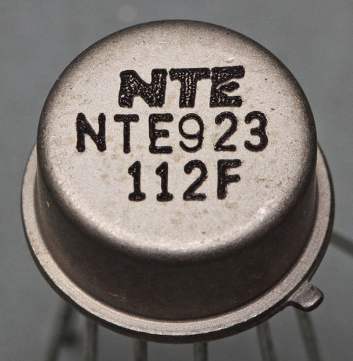
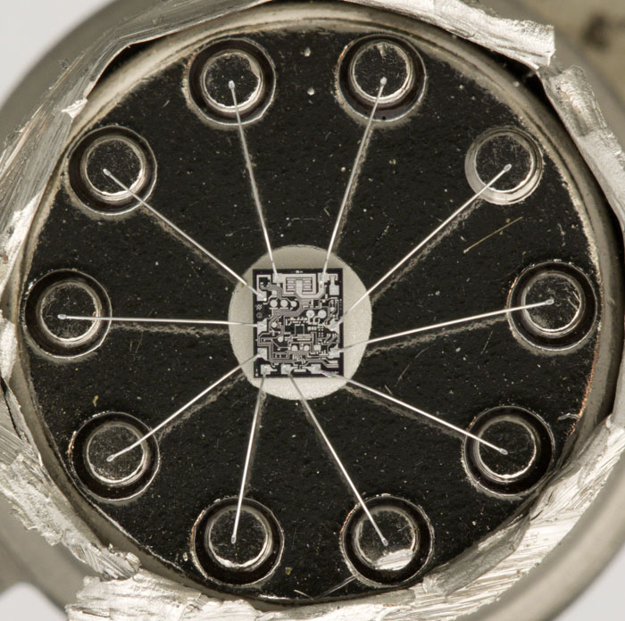


Nothing special on/in the package.
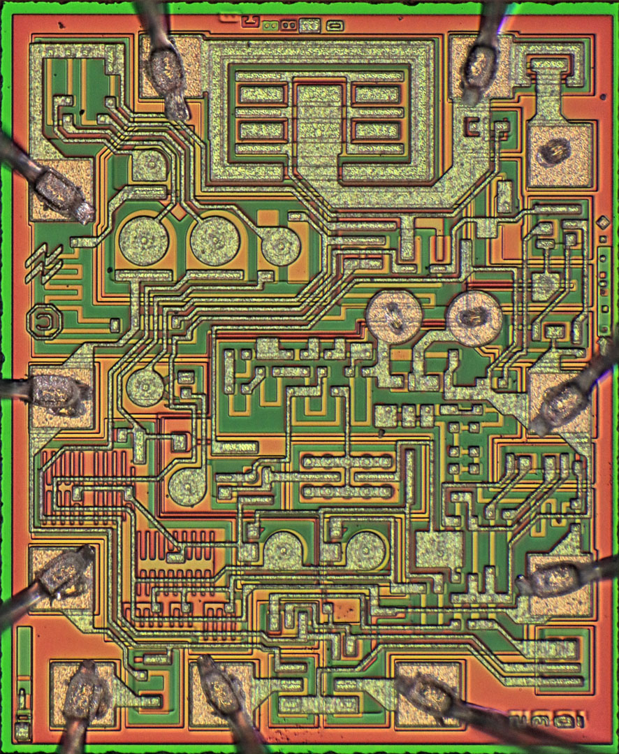


Here we see that NTE uses the bandgap version of the LM723 from National Semiconductor.
(LM723CH: https://www.richis-lab.de/LM723_07.htm // LM723J: https://www.richis-lab.de/LM723_02.htm)

The auxiliary structures are completely the same. Most likely NTE (or ECG) bought up the last batches from National Semiconductor. These could have been finished devices or uncut wafers.
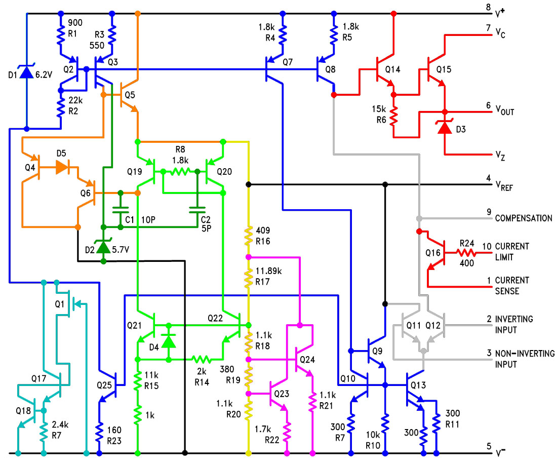


Now let´s take a look at the schematic. In my view the bandgap LM723 does its job like this:

The power section (red) is easy to recognize. Q14 is the driver transistor for the power transistor Q15. D3 is the Z-diode, which in some package is not connected to a pin. Q16 can sink the base current of the driver transistor and thus makes it possible to implement current limiting.

Also easy to recognize is the differential amplifier (gray), which is usually used to compare the actual value of the controlled system with a setpoint. The two input transistors Q11 and Q12 work with the current sink Q13 for this purpose. Q12 sinks the base current of the driver transistor if required.

The current sources and sinks of the device (blue) are current mirrors that use transistor Q2 as a reference. This transistor generates a relatively constant current using the Z-diode D1.
The self-supply is interesting. Via Q7/Q9/Q10/Q25 the transistor Q2 itself sets the current through the Z-diode that is necessary for its operation. To ensure that the circuit starts up safely, there is a small current sink (cyan) in the lower left area.

The reference voltage of the bandgap LM723 is generated with a Brokaw bandgap reference. The core of this reference is formed with the transistors Q21/Q22 with their resistors R14/R15 and the current mirror Q19/Q20 (light green). The current mirror ensures that an equal current flows into both branches. As described with the TL7705 (https://www.richis-lab.de/TL7705.htm), a very temperature-stable voltage is established at the base of Q21 and Q22 if the current densities in the transistors and the resistor values are suitably designed.
The purpose of the diode D4 remains unclear.  :-// It should not become conductive during normal operation. A protection of the base-emitter path against negative voltages does not seem to be necessary due to the high resistance values.

If the desired operating point in the bandgap reference has not yet been reached, the path Q6/D5/Q4 becomes conductive and reduces the current flow through Q5 (orange). Less current flows into the current mirror and into the voltage divider (yellow) of the bandgap reference. As a result, the operating point shifts until the same current flows through the transistors Q21/Q22.

The yellow voltage divider not only controls the transistors Q21/Q22, it also ensures that the desired reference voltage of typically 7,15V is set at the top resistor. The purpose of the transistors Q23/Q24 (purple) remains unclear. It seems that the circuit adds an additional temperature drift. For a Brokaw bandgap reference such an auxiliary circuit should not be necessary.

Capacitors C1 and C2 (dark green) stabilize the bandgap reference. It is interesting to note that the Z-diode D2 in combination with the current source Q3 generates an auxiliary reference for the capacitors. As will be shown this is necessary because the capacitors are not very voltage resistant.
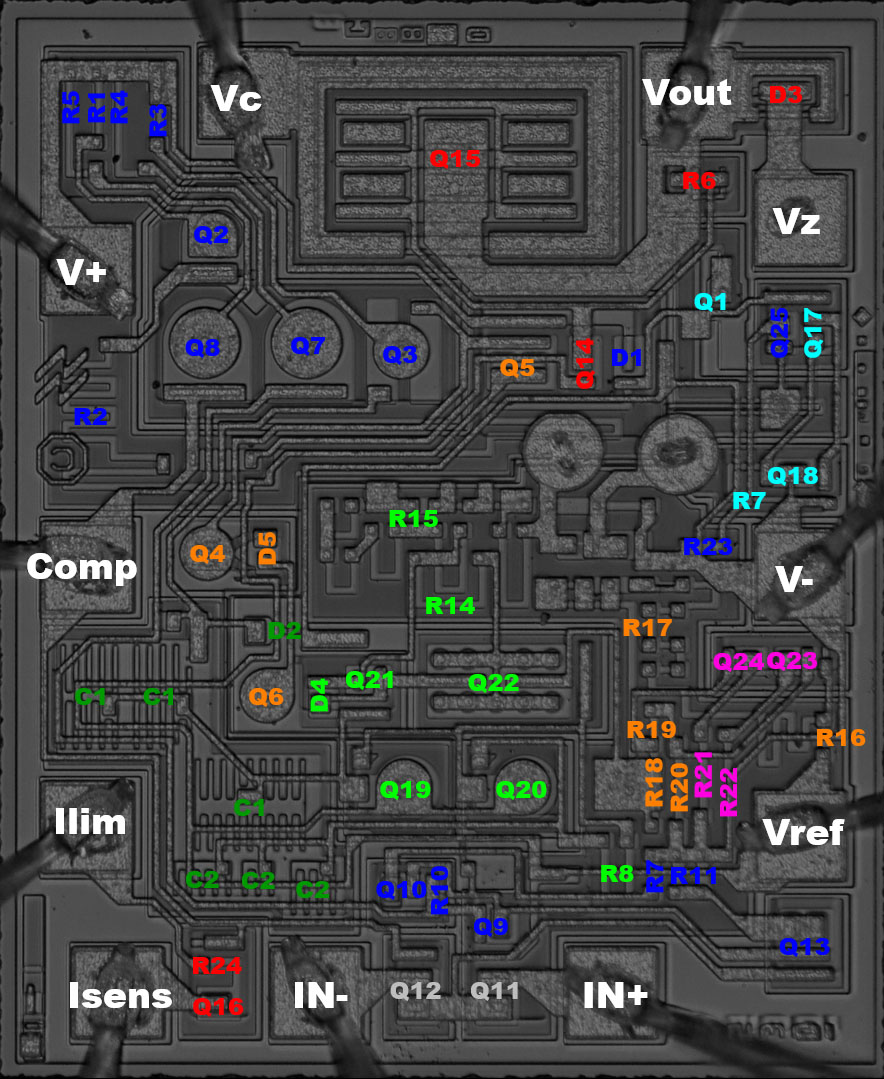


The individual elements can be found on the die as shown in the circuit diagram.
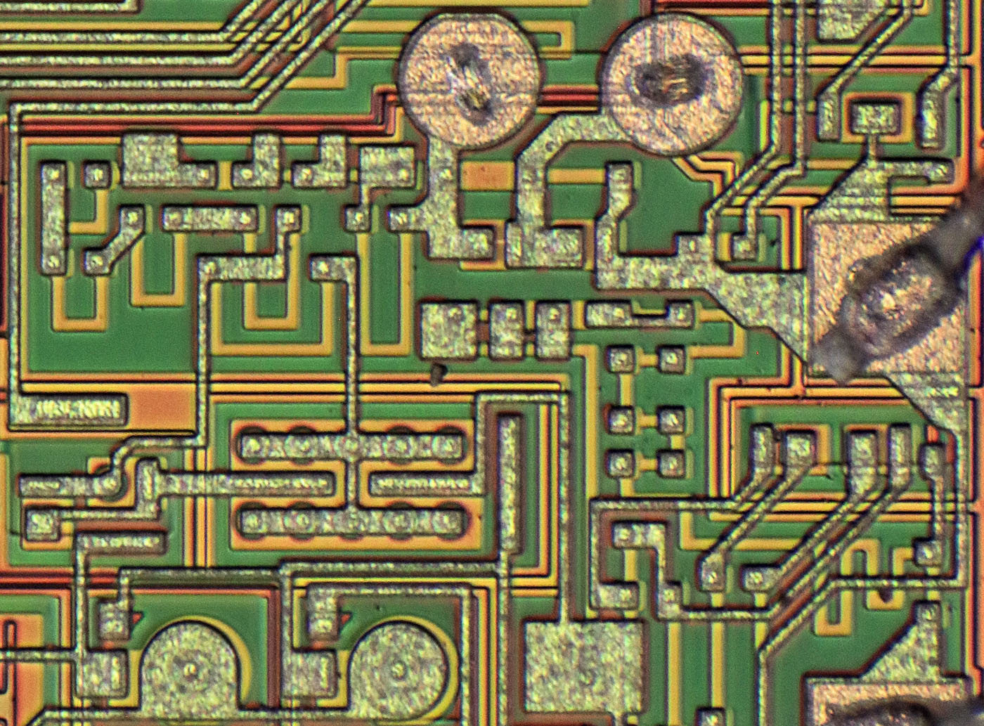


The different sizes of the transistors Q21/Q22 can be seen clearly. The ratio of the emitter areas is 10:1.

As shown in the schematic R15 can be varied to optimize the temperature drift of the bandgap reference. However, it is not just a single resistor that can be added or excluded. The layout would allow many small areas to be bridged with the metal layer. Towards the bottom end two zener fuses are integrated, which allow two resistors to be bridged after fabrication. A thin line can be seen in the left fuse while the right fuse still looks intact.
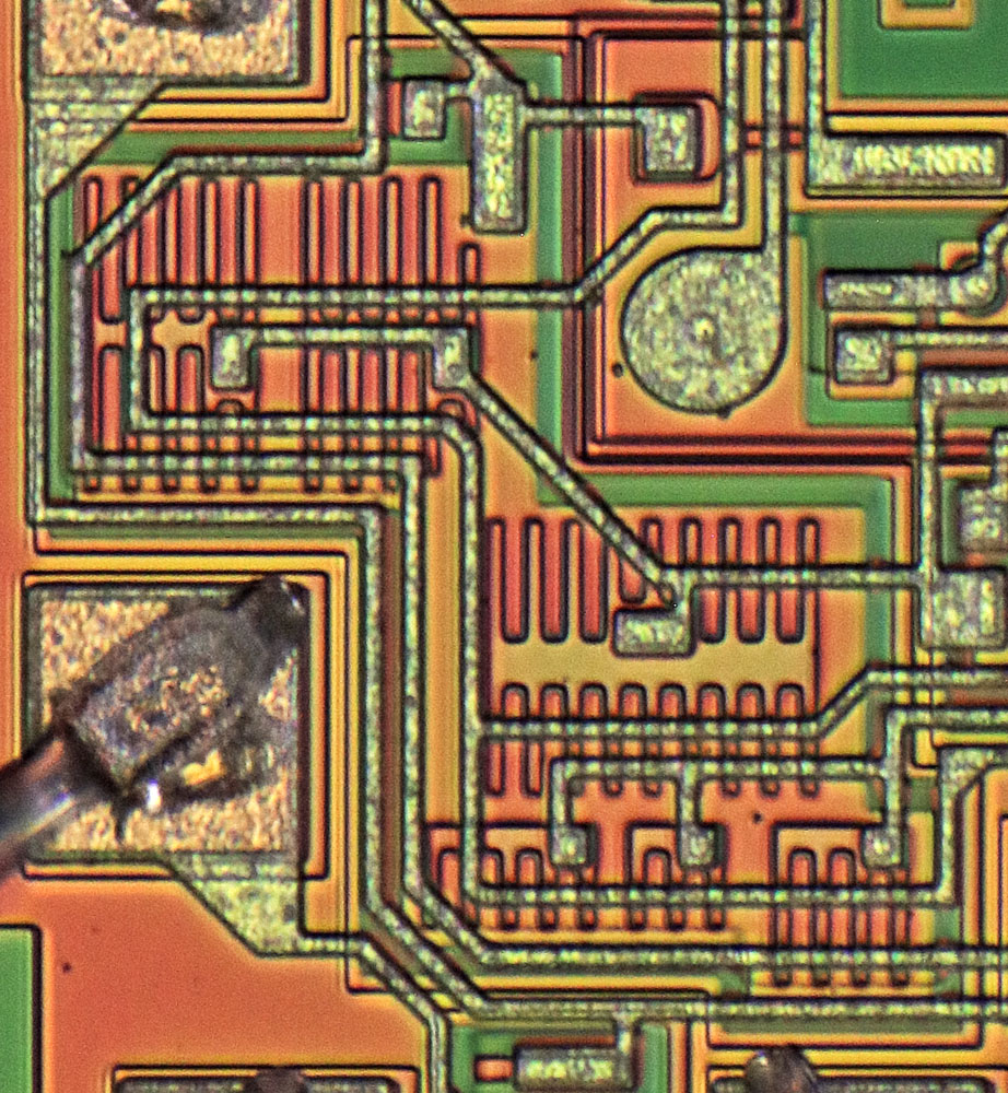


The capacitors are comb-shaped. They are emitter areas in areas with base doping. The special shape ensures higher capacitance because the emitter doping has a certain depth and the comb structure thus increases the surface area.
However, the base-emitter junction has a low breakdown voltage. For this reason, it was necessary to generate a higher auxiliary potential as reference potential for the capacitors.  :-+


https://www.richis-lab.de/LM723_12.htm

 :-/O
 
The following users thanked this post: SeanB, RoGeorge, mawyatt, EJE

Offline magic

  • Super Contributor
  • ***
  • Posts: 6773
  • Country: pl
Re: LM723 die pictures
« Reply #113 on: August 17, 2022, 05:41:42 am »
Pretty much my own conclusion last year - a zener reference is only used for internal biasing. The pink stuff could be some curvature correction or whatnot.

Nice box :wtf:
TI apparently still offers National's version for a little premium, see this part and its datasheet. Dunno if they make new dice or sell remaining stock.
https://www.ti.com/product/LM723QML
 

Offline NoopyTopic starter

  • Super Contributor
  • ***
  • Posts: 1731
  • Country: de
    • Richis-Lab
Re: LM723 die pictures
« Reply #114 on: August 17, 2022, 06:10:51 am »
Pretty much my own conclusion last year - a zener reference is only used for internal biasing. The pink stuff could be some curvature correction or whatnot.

That's how it is.  :-+

A zener to reduce the voltage at the capacitors...  ;D


Nice box :wtf:
TI apparently still offers National's version for a little premium, see this part and its datasheet. Dunno if they make new dice or sell remaining stock.
https://www.ti.com/product/LM723QML

I will have to take a closer look at these...  ;)

Offline magic

  • Super Contributor
  • ***
  • Posts: 6773
  • Country: pl
Re: LM723 die pictures
« Reply #115 on: August 17, 2022, 06:53:02 am »
I'm sure there is nothing interesting in there.

BTW, the link above was some military(?) qualified version or whatnot, here's the ordinary LM723. Still metal cans only.
https://www.ti.com/product/LM723

And TI's own version, in plastic packages.
https://www.ti.com/product/UA723
 

Offline NoopyTopic starter

  • Super Contributor
  • ***
  • Posts: 1731
  • Country: de
    • Richis-Lab
Re: LM723 die pictures
« Reply #116 on: August 17, 2022, 06:56:30 am »
You never know what you will find inside...  ;)

Online iMo

  • Super Contributor
  • ***
  • Posts: 4775
  • Country: pm
  • It's important to try new things..
Re: LM723 die pictures
« Reply #117 on: August 17, 2022, 08:03:28 am »
From an artistic point of view I like the picture above, a kind of "gothic architecture" style.. The newer designs are pure modernism like "art deco"  or "bauhaus" :)
 

Offline NoopyTopic starter

  • Super Contributor
  • ***
  • Posts: 1731
  • Country: de
    • Richis-Lab
Re: LM723 die pictures
« Reply #118 on: August 17, 2022, 08:22:00 am »
I agree with you.  :-+ :D

Offline mawyatt

  • Super Contributor
  • ***
  • Posts: 3250
  • Country: us
Re: LM723 die pictures
« Reply #119 on: August 17, 2022, 01:01:02 pm »
From an artistic point of view I like the picture above, a kind of "gothic architecture" style.. The newer designs are pure modernism like "art deco"  or "bauhaus" :)

Agree, the image noise also adds to the artistic effect. This image could be printed and wall mounted for display!!

Well done and rendered by Noopy as usual :-+

Best,
Curiosity killed the cat, also depleted my wallet!
~Wyatt Labs by Mike~
 
The following users thanked this post: Noopy

Offline NoopyTopic starter

  • Super Contributor
  • ***
  • Posts: 1731
  • Country: de
    • Richis-Lab
Re: LM723 die pictures
« Reply #120 on: August 22, 2022, 11:03:42 am »
At first I thought the 923 is just a special naming NTE had chosen for its 723 but I have found old magazines with prices for a LM923 and on the die of the ST LM723 there are also the numbers 923.

Does anyone know what this 923 is? A 723 with a higher temperature rating?

Offline NoopyTopic starter

  • Super Contributor
  • ***
  • Posts: 1731
  • Country: de
    • Richis-Lab
Re: LM723 die pictures
« Reply #121 on: October 13, 2022, 06:08:04 pm »


Harris Semiconductor produced a variant of the LM723 under the designation CA723. The C marks a slightly worse specified variant. These are approved for a temperature range from 0°C to +70°C (compared to -55°C to +125°C for the variant without C). Nevertheless, the accuracy and stability is slightly worse. The T stands for the metal housing.

Besides the CA723 from Harris Semiconductor, voltage regulators with the same designation can be found from Intersil and RCA. Harris Semiconductor controlled both Intersil and RCA for some time. The earliest references to the CA723 are found in 1978 and are attributed to RCA. Intersil advertises an LM723 as an alternative in 1979. It seems very likely that the CA723 is an RCA development that was adopted by Harris. With the integration of Intersil, the CA723 probably then displaced the Intersil variant of the LM723 as well.


The schematic shown in the Harris Semiconductor datasheet is very similar to the schematic of Fairchild's µA723 (https://www.richis-lab.de/LM723_06.htm).


The housing is connected to the negative supply.


The characters TA6563 at the top edge of the die are probably an internal project designation. The auxiliary structures in the lower right corner are typical for RCA components (CA555: https://www.richis-lab.de/555_11.htm, CA3161: https://www.richis-lab.de/logic22.htm).

The arrangement of the components corresponds to the arrangement in Fairchild's µA723. Some structures, such as the power transistors look exactly the same.


The circuit of the CA723CT from Harris Semiconductor also corresponds to the µA723 from Fairchild. Two errors were found in the Fairchild schematic. Here you can see the corrected Fairchild schematic. The supply of transistor Q11 is already shown correctly in the Harris schematic. However, the supply of transistor Q9 shows the same error as in the original Fairchild schematic. As shown here, it is supplied by the reference voltage, not by the positive supply voltage.


The Fairchild µA723 uses the base-emitter junction of a normal transistor as a Z-diode for generating the reference voltage (left). In the CA723CT (right) a special structure has been integrated for this purpose in which the anode has a much larger area.


https://www.richis-lab.de/LM723_13.htm

 :-/O
 
The following users thanked this post: SeanB, RoGeorge, floobydust, EJE

Offline NoopyTopic starter

  • Super Contributor
  • ***
  • Posts: 1731
  • Country: de
    • Richis-Lab
Re: LM723 die pictures
« Reply #122 on: March 13, 2023, 08:10:51 pm »


Motorola produced a variant of the LM723 with the name MC1723. The MC1723C is specified for an operating temperature range between 0°C and 70°C. The MC1723 without index allows operation between -55°C and 125°C.


Two schematics can be found for the MC1723. The upper schematic is from the Motorola Linear Integrated Circuits Data Book from 1971. More recent datasheets show the lower schematic. Similar to the µA723 built by Fairchild (https://www.richis-lab.de/LM723_06.htm), the supply of the non-inverting branch of the differential amplifier has been relocated. Here, however, a mistake has crept in quite surely. The branch is not only connected to the reference voltage range, but also to the common base of the current sources. The latter makes no sense.


The design of the MC1723 is similar to the other LM723 variants, but there are some interesting differences. It is very different to the design zeptobars has shown.

In the middle of the die a resistor strip is connected to two metal surfaces. Obviously the structure was used to determine the resistor value after manufacturing.

The angles shown with the different masks and a sequence of three letters seem to be typical features of a Motorola design. The same patterns can also be found in the MC1455 (https://www.richis-lab.de/555_13.htm).


In many areas, the circuit corresponds to the circuit diagram. However, there are also some differences. In the right area there are surprisingly many elements that are not included into the circuit.


If you draw the schematic, you will see that the reference current for the biasing is generated quite differently in the MC1723 than in the µA723, for example.


Motorola has printed the metal layer of the MC1723 in the Linear Integrated Circuits Data Book. The structures do not match the present die at all. Either the design was heavily revised or the MC1723 released for the extended operating temperature range contains a completely different design, which was shown here.


https://www.richis-lab.de/LM723_14.htm

 :-/O
 
The following users thanked this post: SeanB, RoGeorge, ch_scr

Offline mediatechnology

  • Newbie
  • Posts: 1
  • Country: us
    • Pro Audio Design Forum
Re: LM723 die pictures
« Reply #123 on: June 24, 2023, 09:15:57 pm »
New here to this forum and just wanted to point out that the µA723 is going to be 55 years old in 2023.

Here are some pretty ones I found in my parts stash along with links to the September 1968 data sheet and a clean copy of the 1968 Application note I scanned.

µA723 Data sheet, September 1968: https://proaudiodesignforum.com/images/pdf/uA723_Data_Sheet_Fairchild_1968.pdf

µA723 Application Note, 1968: https://proaudiodesignforum.com/images/pdf/uA723_Application_Notes_Fairchild_Semiconductor_1968.pdf


Source: https://www.proaudiodesignforum.com/forum/php/viewtopic.php?t=1327
 
The following users thanked this post: blackdog, SeanB, Wolfgang, RoGeorge, ch_scr, Noopy

Offline NoopyTopic starter

  • Super Contributor
  • ***
  • Posts: 1731
  • Country: de
    • Richis-Lab
Re: LM723 die pictures
« Reply #124 on: August 13, 2023, 06:19:46 pm »


Taking a look into the DIL variant of the MAA723, the MAA723CN.
(December 1984)


The edge length is 1,3mm. The die is exactly the same as in the TO variants.


https://www.richis-lab.de/LM723_15.htm

 :-/O
 
The following users thanked this post: SeanB, RoGeorge, ch_scr

Online iMo

  • Super Contributor
  • ***
  • Posts: 4775
  • Country: pm
  • It's important to try new things..
Re: LM723 die pictures
« Reply #125 on: August 14, 2023, 10:50:29 am »
None cracks in the passivation layer this time?
 

Offline NoopyTopic starter

  • Super Contributor
  • ***
  • Posts: 1731
  • Country: de
    • Richis-Lab
Re: LM723 die pictures
« Reply #126 on: August 14, 2023, 10:51:15 am »
No, nothing to see...  :-+

Offline NoopyTopic starter

  • Super Contributor
  • ***
  • Posts: 1731
  • Country: de
    • Richis-Lab
Re: LM723 die pictures
« Reply #127 on: October 08, 2023, 07:27:50 pm »


Lambda Semiconductors called their LM723 variant LAS723.


The edge length of the die is 1,9mm. The design is not comparable with any of the designs I have documented so far. Nevertheless, the arrangement of the function blocks is similar. Current sources are located in the upper left corner. The output transistor is integrated at the upper edge. There, however, the Z-diode has been omitted, which is usually connected in series to the output transistor. In the lower right corner there is a voltage reference block. But this is much more complex than on most other LM723.


The detail shows that this is a bandgap reference, not the more common temperature compensated zener diode. In the lower right corner, you can clearly see the typical arrangement of a large and a small transistor. The large transistor contains four of the emitter areas of the small transistor. The emitters are connected to a whole series of resistors which determine the temperature drift of the reference voltage. To be able to adjust this temperature drift exactly, the design offers many possibilities to adjust the resistor values. Contacts between metal layer and silicon can be moved and shorting bridges can be set or removed. In the lower left corner of this picture you can see the current mirror that supplies the bandgap transistors.


https://www.richis-lab.de/LM723_16.htm

 :-/O
 
The following users thanked this post: SeanB, RoGeorge

Offline magic

  • Super Contributor
  • ***
  • Posts: 6773
  • Country: pl
Re: LM723 die pictures
« Reply #128 on: October 08, 2023, 09:29:30 pm »
The detail shows that this is a bandgap reference, not the more common temperature compensated zener diode. In the lower right corner, you can clearly see the typical arrangement of a large and a small transistor.
Actually, in the bottom right corner, I can see the VREF contact pad and a zener diode right above it ;)

But the rest is indeed a Brokaw cell bandgap reference. The zener clamps its output so it can't go too high above ground.

What's weird is that output voltage of the Brokaw cell is one diode below VREF (if I counted all the emitter followers correctly) so VREF is clamped to zener voltage plus diode drop, which is about the normal output voltage of 723 regulator. I suppose the zener has slightly higher breakdown and remains inactive except under transient conditions when the bandgap cell is too slow to react or whatever, otherwise it would be seriously weird...
 

Offline NoopyTopic starter

  • Super Contributor
  • ***
  • Posts: 1731
  • Country: de
    • Richis-Lab
Re: LM723 die pictures
« Reply #129 on: October 09, 2023, 03:07:34 am »
Actually, in the bottom right corner, I can see the VREF contact pad and a zener diode right above it ;)

Yes there is a zener.  ;D
I assume this zener diode is actually used as a pn capacitor. That would also explain why it is so big. And the locaction would be good for some capacitance.


But the rest is indeed a Brokaw cell bandgap reference. The zener clamps its output so it can't go too high above ground.

I don´t see this...  :-//


What's weird is that output voltage of the Brokaw cell is one diode below VREF (if I counted all the emitter followers correctly) so VREF is clamped to zener voltage plus diode drop, which is about the normal output voltage of 723 regulator. I suppose the zener has slightly higher breakdown and remains inactive except under transient conditions when the bandgap cell is too slow to react or whatever, otherwise it would be seriously weird...

In my view the VREF output is connected to a voltage divider and this divider defines the multiplicator of the bandgap voltage. Like we have often seen in voltage references..

Offline magic

  • Super Contributor
  • ***
  • Posts: 6773
  • Country: pl
Re: LM723 die pictures
« Reply #130 on: October 09, 2023, 06:19:15 am »
Okay, PaintCAD® again :D

Black is ground.
Pink is the zener and a compensation capacitor ;)
Red/magenta is the bandgap NPNs and emitter resistors.
Orange is PNP buffers.
Yellow is the active load.
Green is load for the orange buffers and a first level shift.
Cyan is more level shift and active load (outside the view).
Blue is the VREF output darlington.
Violet is current limiting.
Brown is the feedback divider.

VREF voltage is Brokaw output voltage (red collector) + orange Vbe + green Vbe + cyan resistor drop + cyan diode - 2x blue Vbe.
Approximately it's red collector + 1x Vbe + cyan resistor drop, so red collector is a bit less than one Vbe below VREF. And the zener clamps this voltage.


edit
I'm not saying that this is not a bandgap reference, pretty surely the BG circuit wouldn't be here if it weren't regulating the output voltage.
But the zener is reverse biased close to breakdown and appears to really be a zener and not just capacitance.
It may be handling edge cases like startup, load transients, VCC transients, although I can't imagine what exactly it does :-//
« Last Edit: October 09, 2023, 06:31:15 am by magic »
 
The following users thanked this post: RoGeorge, schmitt trigger, Noopy

Offline NoopyTopic starter

  • Super Contributor
  • ***
  • Posts: 1731
  • Country: de
    • Richis-Lab
Re: LM723 die pictures
« Reply #131 on: October 09, 2023, 07:36:39 pm »
Well done!

I agree with you.  :)

And it is a LM723 with a bandgap reference.  ;D

Online iMo

  • Super Contributor
  • ***
  • Posts: 4775
  • Country: pm
  • It's important to try new things..
Re: LM723 die pictures
« Reply #132 on: October 09, 2023, 08:01:12 pm »
LAS723' Vref is 2.5V only..
 
The following users thanked this post: Wolfgang, magic, Noopy

Offline magic

  • Super Contributor
  • ***
  • Posts: 6773
  • Country: pl
Re: LM723 die pictures
« Reply #133 on: October 10, 2023, 06:00:25 am »
This explains a few things, such as why a bandgap reference was used and why the ratio of feedback resistors doesn't seem large. I noticed it but somehow haven't thought about it long enough to realize the obvious...

The zener is obviously not close to breakdown, then. Still not sure why it's there.

Could it be they also had a 7V version which only differed in metal layer? (Probably not, bias current of the zener would be low and poorly controlled, unless some of the bandgap components were reused to make a load for it).
« Last Edit: October 10, 2023, 06:07:17 am by magic »
 

Offline NoopyTopic starter

  • Super Contributor
  • ***
  • Posts: 1731
  • Country: de
    • Richis-Lab
Re: LM723 die pictures
« Reply #134 on: October 10, 2023, 06:23:55 am »
Yes, that explains a lot.

I assume you are just on the wrong track. It's just a pn capacitor, not a zener diode.  ^-^

Offline Wolfgang

  • Super Contributor
  • ***
  • Posts: 1775
  • Country: de
  • Its great if it finally works !
    • Electronic Projects for Fun
Re: LM723 die pictures
« Reply #135 on: October 10, 2023, 06:55:52 am »
Well done!

I agree with you.  :)

And it is a LM723 with a bandgap reference.  ;D

Maybe similar (but not the same) than the SG3532 regulator. This also has a 2.5V reference.
 

Offline NoopyTopic starter

  • Super Contributor
  • ***
  • Posts: 1731
  • Country: de
    • Richis-Lab
Re: LM723 die pictures
« Reply #136 on: October 10, 2023, 10:15:31 am »
Well done!

I agree with you.  :)

And it is a LM723 with a bandgap reference.  ;D

Maybe similar (but not the same) than the SG3532 regulator. This also has a 2.5V reference.

We should take a look inside the SG3532.  :-/O 8)
 
The following users thanked this post: Wolfgang

Offline p.larner

  • Frequent Contributor
  • **
  • !
  • Posts: 690
  • Country: gb
Re: LM723 die pictures
« Reply #137 on: October 11, 2023, 10:37:24 pm »
some pics of the infinion SG3532 would be good to compair.
 

Offline NoopyTopic starter

  • Super Contributor
  • ***
  • Posts: 1731
  • Country: de
    • Richis-Lab
Re: LM723 die pictures
« Reply #138 on: October 12, 2023, 03:12:17 am »
some pics of the infinion SG3532 would be good to compair.

I will do so. The question is which manufacturer and where to get it. It seems like the first one is from Silicon General. I will get one built by Microsemi.


But first we have a LM723 built by Samsung! No index is shown on this part. However, the datasheet specifies two variants. Index C is specified for an operating voltage range of 0°C to 70°C. Index I is specified for an operating voltage range of -25°C to 85°C. Index I is specified for an operating voltage range of -25°C to 85°C.


The dimensions of the dies are 1,4mm x 1,3mm. KA723 could be an internal designation. The circuit shows the division of the circuit parts known from many other 723 variants. Nevertheless, the design seems to be their own.


https://www.richis-lab.de/LM723_17.htm

 :-/O
 
The following users thanked this post: SeanB, RoGeorge

Offline magic

  • Super Contributor
  • ***
  • Posts: 6773
  • Country: pl
Re: LM723 die pictures
« Reply #139 on: October 12, 2023, 04:29:41 am »
KA was the usual prefix of old Samsung parts. KA358, KA317, KA555, KA5532, etc.
You can still find those datasheets.

BTW, Samsung sold their semiconductor division to Fairchild (the new Fairchild, spun off from National) so sometimes the prefix can also be found on Fairchild branded parts. New Fairchild started as National's discrete transistors division, and IIRC all their IC products came from acquisitions - mainly aforementioned Samsung and Raytheon, giving a mix of KA and RC parts, until Fairchild mostly renamed them more conventionally.
« Last Edit: October 12, 2023, 04:35:43 am by magic »
 
The following users thanked this post: Noopy

Offline NoopyTopic starter

  • Super Contributor
  • ***
  • Posts: 1731
  • Country: de
    • Richis-Lab
Re: LM723 die pictures
« Reply #140 on: October 12, 2023, 04:35:57 am »
KA was the usual prefix of old Samsung parts. KA358, KA317, KA555, KA5532, etc.

Now that you have written this it seems familiar.  :-+

Online iMo

  • Super Contributor
  • ***
  • Posts: 4775
  • Country: pm
  • It's important to try new things..
Re: LM723 die pictures
« Reply #141 on: October 12, 2023, 07:28:42 am »
It is interesting the wiring complexity of the LAS part vs the others (usually clones). I wonder what are the addons or diffs (except the bandgap) in the LAS part.. There is "the thermal overload protection" mentioned in the DS, for example, but it should be more, imho.
« Last Edit: October 12, 2023, 07:30:37 am by iMo »
 

Offline magic

  • Super Contributor
  • ***
  • Posts: 6773
  • Country: pl
Re: LM723 die pictures
« Reply #142 on: October 12, 2023, 08:12:48 am »
Maybe your turn to post some schematic :P
It's a simple chip, only a little tedious due to that maze of wires.

There is clearly the differential amp to the left of the reference with its tail current sink nearby, and the whole left edge is bias generation. Output stage at the top, and not much is left.
 
The following users thanked this post: iMo

Offline Wolfgang

  • Super Contributor
  • ***
  • Posts: 1775
  • Country: de
  • Its great if it finally works !
    • Electronic Projects for Fun
Re: LM723 die pictures
« Reply #143 on: October 12, 2023, 08:23:26 am »
Well done!

I agree with you.  :)

And it is a LM723 with a bandgap reference.  ;D

Maybe similar (but not the same) than the SG3532 regulator. This also has a 2.5V reference.

We should take a look inside the SG3532.  :-/O 8)

Hi,

do you have a SG3532 chip at hand ?

Wolfgang
 

Offline NoopyTopic starter

  • Super Contributor
  • ***
  • Posts: 1731
  • Country: de
    • Richis-Lab
Re: LM723 die pictures
« Reply #144 on: October 12, 2023, 03:22:00 pm »
I wouldn't expect something special in the LAS723 either. The bandgap makes the circuit bigger.

I hope to get a SG3532 built by Microsemi but not sure yet.

Offline Dan123456

  • Regular Contributor
  • *
  • Posts: 199
  • Country: au
Re: LM723 die pictures
« Reply #145 on: October 13, 2023, 01:30:31 am »
Woah… this stuff is so cool!!!

Absolutely beautiful stuff all  :D

Apologies if this has been covered somewhere before but, how do you guys do this?

I had never heard of this process before so just googled “delidding ics” (as closest thing I knew of was removing the heat spreader from CPU’s) and found an awesome video from Applied Science where he was using fuming nitric acid.

He said he wasn’t sure if it had to be fuming nitric or if it could just be good old “regular” 68% concentrated nitric?

I would love to give this a go as your results look so cool but don’t stock any RFNA / WFNA and don’t really like making it (68% is more than good enough for my uses! ) :P
 

Offline NoopyTopic starter

  • Super Contributor
  • ***
  • Posts: 1731
  • Country: de
    • Richis-Lab
Re: LM723 die pictures
« Reply #146 on: October 13, 2023, 03:04:06 am »
You find a lot of information about decapping in a lot of places.

We have discussed the decapping here:
https://www.eevblog.com/forum/projects/decapping-and-chip-documentation-howto/msg2663778/#msg2663778

My website has a own section:
https://www.richis-lab.de/Howto.htm
(Google translator is your friend)

I´m from europe. We don´t get nitric or sulfuric acid not even in low concentrations. Because of that I started burning the epoxy. With my furnace the sucess rate is quite high.  :-/O

Read what we have written and after that feel free to ask whatever you want.  :-+
 
The following users thanked this post: Dan123456

Offline p.larner

  • Frequent Contributor
  • **
  • !
  • Posts: 690
  • Country: gb
Re: LM723 die pictures
« Reply #147 on: October 13, 2023, 03:21:30 am »
i got the infinion chip from ebay,its a ceramic job so hard to decapitate i guess,needs a lot less volts on the current sense so has more transistors in that section,or a darlington i guess.
 

Offline NoopyTopic starter

  • Super Contributor
  • ***
  • Posts: 1731
  • Country: de
    • Richis-Lab
Re: LM723 die pictures
« Reply #148 on: October 13, 2023, 03:28:06 am »
i got the infinion chip from ebay,its a ceramic job so hard to decapitate i guess,needs a lot less volts on the current sense so has more transistors in that section,or a darlington i guess.

Is it really infineon? I would assume it´s linfinity?

I now will get one from Silicon General. Looking at the naming this could be the first one.

Ceramic is easy to decap. Just knock with a screwdriver against the material between the two ceramic parts and it will fall in pieces. ...ok a little experience helps...  ;)

Offline magic

  • Super Contributor
  • ***
  • Posts: 6773
  • Country: pl
Re: LM723 die pictures
« Reply #149 on: October 13, 2023, 05:04:47 am »
He said he wasn’t sure if it had to be fuming nitric or if it could just be good old “regular” 68% concentrated nitric?

I would love to give this a go as your results look so cool but don’t stock any RFNA / WFNA and don’t really like making it (68% is more than good enough for my uses! ) :P
If you don't feel like reading the whole thread linked by Noopy, and I'm not even 100% sure if I ever described it in detail:

Pour 1~2ml into a 5ml beaker, drop the chip, cover with watch glass or at least HDPE bottle cap (for vapor reflux, reduces fuming and loss of acid).
Boil gently for a few minutes. Nitric acid remains transparent, allowing you to watch progress, only turns green from dissolved copper.

68% will eat exposed aluminium bonding pads, but won't reach under the passivation glass in short time. FNA passivates aluminium, hence the preference.

edit: Hopefully you know it already, but NO₂ is poison and stinks ugly like chlorine, so don't be an idiot, do it outside ;D
« Last Edit: October 13, 2023, 05:15:21 am by magic »
 
The following users thanked this post: Dan123456

Offline Dan123456

  • Regular Contributor
  • *
  • Posts: 199
  • Country: au
Re: LM723 die pictures
« Reply #150 on: October 13, 2023, 07:04:41 am »
He said he wasn’t sure if it had to be fuming nitric or if it could just be good old “regular” 68% concentrated nitric?

I would love to give this a go as your results look so cool but don’t stock any RFNA / WFNA and don’t really like making it (68% is more than good enough for my uses! ) :P
If you don't feel like reading the whole thread linked by Noopy, and I'm not even 100% sure if I ever described it in detail:

Pour 1~2ml into a 5ml beaker, drop the chip, cover with watch glass or at least HDPE bottle cap (for vapor reflux, reduces fuming and loss of acid).
Boil gently for a few minutes. Nitric acid remains transparent, allowing you to watch progress, only turns green from dissolved copper.

68% will eat exposed aluminium bonding pads, but won't reach under the passivation glass in short time. FNA passivates aluminium, hence the preference.

edit: Hopefully you know it already, but NO₂ is poison and stinks ugly like chlorine, so don't be an idiot, do it outside ;D

Awesome! Thanks so much to both you and Noopy  :D

I’ve been reading through all the info and am super keen to give this a go! Thank you  :)

I would probably go down the chemical route as am more confident in my chemistry skills than I am with my electronics ones at this point think  :P To be completely honest, I think I would probably be far more likely to kill myself wiring up a furnace than I would working with most chemicals with a LD50 higher than cyanide :-DD

I am already thinking of maybe experimenting with a few different acids or solutions such as maybe testing out if H3PO4 works (might be an easy-to-find replacement for people in countries that don’t have access to HNO3 / H2SO4?)  :)

Agree! NO2 is some pretty nasty stuff! I have caught a lung full from being stupid once or twice and straight up thought I was dying  :-DD

That said, Noopy mentioned HF in the other thread… now that stuff… that stuff proper terrifies me!!!  :-/O
 

Offline NoopyTopic starter

  • Super Contributor
  • ***
  • Posts: 1731
  • Country: de
    • Richis-Lab
Re: LM723 die pictures
« Reply #151 on: October 13, 2023, 02:03:48 pm »
People have tried a lot but unfortunately it seems that just sulfuric and nitric acid do the job.
Nevertheless feel free to find a new and more convenient way to open packages. I will buy you a beer and a lot of other people too.  :popcorn: :-+ ;D

HF is really nasty. I just use it as Armour Etch (glass etching) since housewifes are allowed to use it.  ;D
 
The following users thanked this post: Dan123456

Offline NoopyTopic starter

  • Super Contributor
  • ***
  • Posts: 1731
  • Country: de
    • Richis-Lab
Re: LM723 die pictures
« Reply #152 on: November 26, 2023, 06:51:54 pm »


The Motorola MC1723 was offered in different package variants. The index G stands for the TO package shown here. The additional index C is missing, which shows that the device is specified for the extended operating temperature range of -55°C to 125°C.


The die features the same circuit design as the MC1723C (https://www.richis-lab.de/LM723_14.htm).


https://www.richis-lab.de/LM723_18.htm

 :-/O
 
The following users thanked this post: SeanB, RoGeorge, MK14, iMo

Online iMo

  • Super Contributor
  • ***
  • Posts: 4775
  • Country: pm
  • It's important to try new things..
Re: LM723 die pictures
« Reply #153 on: November 26, 2023, 07:06:50 pm »
 :D I've been using the Motorola 1723 in DIP in my ADR1001#1 ref..
 

Offline NoopyTopic starter

  • Super Contributor
  • ***
  • Posts: 1731
  • Country: de
    • Richis-Lab
Re: LM723 die pictures
« Reply #154 on: November 26, 2023, 07:15:43 pm »
:D I've been using the Motorola 1723 in DIP in my ADR1001#1 ref..

The 1723 as a substitute for the ADR1001?  ;D

Online iMo

  • Super Contributor
  • ***
  • Posts: 4775
  • Country: pm
  • It's important to try new things..
Re: LM723 die pictures
« Reply #155 on: November 26, 2023, 07:22:57 pm »
Yep, but do not tell anyone..  :P
 

Offline NoopyTopic starter

  • Super Contributor
  • ***
  • Posts: 1731
  • Country: de
    • Richis-Lab
Re: LM723 die pictures
« Reply #156 on: January 08, 2024, 04:40:58 am »
some pics of the infinion SG3532 would be good to compair.

I have uploaded a SG3532!
I have put it in the voltage regulator thread:

https://www.eevblog.com/forum/projects/voltage-regulators-die-pictures/msg5265990/#msg5265990

https://www.richis-lab.de/voltageregulator23.htm

 :-/O
 
The following users thanked this post: Wolfgang


Share me

Digg  Facebook  SlashDot  Delicious  Technorati  Twitter  Google  Yahoo
Smf