Author Topic: Logic-ICs - die pictures  (Read 13309 times)

0 Members and 1 Guest are viewing this topic.

Offline NoopyTopic starter

  • Super Contributor
  • ***
  • Posts: 1726
  • Country: de
    • Richis-Lab
Logic-ICs - die pictures
« on: January 25, 2021, 09:34:49 pm »
Let´s take a look into some logic ICs.
You can find an overview here: https://www.richis-lab.de/logic.htm


First logic IC is a CPLD, a Lattice ispLSI1016.
The LSI1016 is the smallest CPLD of this model range. The isp variant can be programmed in circuit.
16 logic blocks, 2000 gates, 96 register, 36 I/Os, max 80MHz, max delay 15ns


The die is quite big: 6,1mm x 4,1mm
The datasheet states that the ispLSI1016 was manufactured with a 0,8µm process. Challanging my capabilities.  :-/O ;D


A 1992 design.


A first revision?
Quite a lot of masks.


In the dicing area there are quite some symbols and test structures.


Developer initials?  :-//


Here you can see an I/O bondpad. On the top of the bondpad there is the input structure. At the left and the right sides of the bondpad there are the Push-Pull-transistors.


Here you can see an input stage. I assume the big structures are clamping diodes. Behind the clamping diodes there is a small resistor and a transistor probably acting as a pull-up or pull-down.


The structures are quite small but you can identify the big functional blocks.


There are a lot of small structures between the bondpads which probably do some housekeeping.
Here you can see one of the more interesting circuits. Perhaps a small memory? Perhaps a multiplexer for connecting the distributed memory cells?


Global logic block and I/O cell. Between the two you can spot the 16 lines of the output routing pool.
(Quite likely, you can´t be 100% sure.)


Global logic block input logic array.


Global routing pool, in there are quite a lot of interconnections with their memory cells.


More pictures here:
https://www.richis-lab.de/logic01.htm

 :-/O
 
The following users thanked this post: SeanB, edavid, RoGeorge, Miyuki, jxjbsd

Online ataradov

  • Super Contributor
  • ***
  • Posts: 11234
  • Country: us
    • Personal site
Re: Logic-ICs - die pictures
« Reply #1 on: January 25, 2021, 09:49:49 pm »
SJDC - San Jose Design Center.
Alex
 
The following users thanked this post: Noopy

Online RoGeorge

  • Super Contributor
  • ***
  • Posts: 6177
  • Country: ro
Re: Logic-ICs - die pictures
« Reply #2 on: January 25, 2021, 10:27:20 pm »
Thank you, subscribed!   :popcorn:

Offline exe

  • Supporter
  • ****
  • Posts: 2562
  • Country: nl
  • self-educated hobbyist
Re: Logic-ICs - die pictures
« Reply #3 on: January 26, 2021, 05:55:59 pm »
A first revision?
Quite a lot of masks.

So, masks are used to amend errors on photo templates?
 

Online ataradov

  • Super Contributor
  • ***
  • Posts: 11234
  • Country: us
    • Personal site
Re: Logic-ICs - die pictures
« Reply #4 on: January 26, 2021, 06:01:38 pm »
No, by "masks" he meant the photo template. That's how they are called in the industry.

Each test structure represents one mask. And this is a lot indeed. But configurable devices are complex in their design.
Alex
 

Offline NoopyTopic starter

  • Super Contributor
  • ***
  • Posts: 1726
  • Country: de
    • Richis-Lab
Re: Logic-ICs - die pictures
« Reply #5 on: February 23, 2021, 01:36:37 pm »


D146, a BCD/7-segment decoder built by HFO.


3,0mm x 1,8mm


Test-transistor...  :-/O


The SN7446 datasheet contains a logical schematic (Texas Instruments, 1988).


Well we find everything shown in the shematic.
The two input gates at the inputs A-D are marked in pink. The purple squares are the output transistors of the eight gates.
Between the inputs you see the lamptest circuit (green) and the blanking circuit (black).
The outputs of the input gates are connected to the decoder matrix (dark green) containing both, the connection matrix and the AND-gates. The big gate of the blanking circuit is placed in this area too. The blue parts are the pull-up-resistors for the decoder.
On top of the decode area there are seven NOR-gates with two or three inputs (orange). There are yellow pull-up-resistors and the last parts are the output transistors (red).


Here you can see the input gates.
The first gates are built with an input stage (buffer or AND), a phase splitter and an output lowside transistor. There is no highside transistor but there is a diode connecting the pull-up-resistor of the phase splitter to the output. In the second gates they spared the phase splitter.
The input of the gates are built with transistors with big base areas in which there are one (buffer) or two (AND) emitter areas forming the inputs. The buried collector is the output of the gate input stage.


In the middle of the die there is the decoder containing 19 multi emitter transistors.


The upper contact is connected to the collector. The lower contact is connected to the base area. In the base area there are some emitters connected to the outputs of the input gates.
There is one rotated transistor. That´s the big gate for the blanking of the 0. This gate works with the same input signals so it was reasonable to place the gate in this area.


You can spot every logical connection formed with a emitter and its contact.
But what´s that? There is an additional connection not shown in the SN7445 datasheet: B1/a2


With this connection you get two more segments.
In my view that 6 looks better.  ;D


Here you see the seven NOR-gates and the output transistors.


Nothing special...
There is an substrate connection at every transistor to prevent ground bouncing in the die.


https://www.richis-lab.de/logic02.htm

 :-/O
 
The following users thanked this post: SeanB, ebclr, doktor pyta, RoGeorge

Offline NoopyTopic starter

  • Super Contributor
  • ***
  • Posts: 1726
  • Country: de
    • Richis-Lab
Re: Logic-ICs - die pictures
« Reply #6 on: February 23, 2021, 05:15:26 pm »
Minor corrections:


Compared to the 7446 there are two additional connections (yellow).


Symbol 6 and symbol 9 are different to the 7446. Symbol 12 is not different.


=> The D146 is more like a 74246 not like a 7446.  :-+

 
The following users thanked this post: exe

Offline NoopyTopic starter

  • Super Contributor
  • ***
  • Posts: 1726
  • Country: de
    • Richis-Lab
Re: Logic-ICs - die pictures
« Reply #7 on: March 14, 2021, 09:27:22 pm »


Now let´s take a look into a ispLSI1024.


The LSI1024 has one megablock more than the LSI1016.


The die is 6,5mm x 5,8mm.


A lot of test structures.


There are also some more complex structures in the slicing area.


The LSI1024 was designed in 1991 while the LSI1016 was designed in 1992 (perhaps the second revision?).


HD24-00, the first revision of the "HD24"?


Push/Pull-Transistors and input protection at the bondpads.


...
A lot of small circuits are placed in the bondpad area.


The LSI1024 is quite similar to the LSI1016 but here we have a third megablock. Since the third megablock is cut in two pieces they needed an additional connection line in the upper area.


Let´s take a look into one of the eight segments of the megablock.


Here there should be two I/O cells.


Global-Logic-Block


Global-Logic-Block connection array


Global-Routing-Pool


Some more pictures:

https://www.richis-lab.de/logic03.htm

 :-/O
 
The following users thanked this post: SeanB, daqq, RoGeorge, Miyuki

Offline aheid

  • Regular Contributor
  • *
  • Posts: 245
  • Country: no
Re: Logic-ICs - die pictures
« Reply #8 on: March 15, 2021, 02:13:16 am »
Love your threads, excellent stuff! Very interesting to look under the bonnet, so to speak.
 

Offline NoopyTopic starter

  • Super Contributor
  • ***
  • Posts: 1726
  • Country: de
    • Richis-Lab
Re: Logic-ICs - die pictures
« Reply #9 on: March 15, 2021, 04:08:37 am »
Thanks for the positive feedback!  :-+ That keeps me taking more pictures.  8)

Offline NoopyTopic starter

  • Super Contributor
  • ***
  • Posts: 1726
  • Country: de
    • Richis-Lab
Re: Logic-ICs - die pictures
« Reply #10 on: April 11, 2021, 09:23:58 pm »
I have some different controller periphery chips. Will post them here.


Mitsubishi M5L8288, a bus controller for a 8086 processor.


Two bondwires for the supply. The seven command outputs can sink more than 220mA. That is not too much for one bondwire but the voltage drop can cause switching problems.


Mitsubishi used two metal layers.


The name of the design?


Some symbols to check the production quality.


Around the die the two metal layers distribute the supply voltage.


The command outputs. Between the bondpads there are the big lowside transistors. On the left side of the bondpads there are the smaller highside transistors.
Wide metal stripes supply the outputs.


Here we have one of the weaker outputs. The lowside transistor (right of the bondpad) is bigger than the highside transistor (above the bondpad) but both are smaller than the transistors of the command outputs.


https://www.richis-lab.de/chipset01.htm

 :-/O
 
The following users thanked this post: SeanB, RoGeorge, Miyuki, schmitt trigger

Offline NoopyTopic starter

  • Super Contributor
  • ***
  • Posts: 1726
  • Country: de
    • Richis-Lab
Re: Logic-ICs - die pictures
« Reply #11 on: April 19, 2021, 02:07:54 pm »


ispLSI1048E, the biggest CPLD of the LSI10xx family. The index E is a an update of the index C which is an update of the ispLSI1048.


Although the ispLSI1048E is much more complex than the ispLSI1024 (https://www.richis-lab.de/logic03.htm) the die is smaller: 5,9mm x 4,7mm. It´s clearly a newer design.


Yes, designed seven years after the ispLSI1024.
The lines are clearly thinner.


There are circuits between the bonpads as we have seen in the smaller CPLDs.


The LSI1048 consists of six megablocks each built with eight GLBs (global logic blocks). The 48 GLBs are placed in groups of four on the left and on the right side of the die.
The GRP (global routing pool) is integrated in the middle of the die.


Here you see a group of four GLBs with it´s portion of the GRP.


GLB


GLB logic array


GRP


I don´t know why the GRP is not symmetrical. Well we don´t know how it is partitioned.


https://www.richis-lab.de/logic04.htm

 :-/O
 
The following users thanked this post: SeanB, daqq, RoGeorge, Miyuki

Online Alex Eisenhut

  • Super Contributor
  • ***
  • Posts: 3335
  • Country: ca
  • Place text here.
Re: Logic-ICs - die pictures
« Reply #12 on: April 19, 2021, 03:43:58 pm »
These pictures are ... to "die" for!

 :-DD
Hoarder of 8-bit Commodore relics and 1960s Tektronix 500-series stuff. Unconventional interior decorator.
 

Offline NoopyTopic starter

  • Super Contributor
  • ***
  • Posts: 1726
  • Country: de
    • Richis-Lab
Re: Logic-ICs - die pictures
« Reply #13 on: May 02, 2021, 01:01:39 am »
...
D146, a BCD/7-segment decoder built by HFO.
...


The D147 does the same as the D146 but the maximum output voltage is only 15V (vs. 30V of the D146).


As we would have expected the design of the die is the same. Probably they did some binning.


There is a small defect in the metal layer above one of the output transistors.


And a nice pictures of the test-transistor.  :-/O


https://www.richis-lab.de/logic02.htm

 :-/O
 
The following users thanked this post: SeanB, xrunner, Miyuki

Offline NoopyTopic starter

  • Super Contributor
  • ***
  • Posts: 1726
  • Country: de
    • Richis-Lab
Re: Logic-ICs - die pictures
« Reply #14 on: May 14, 2021, 07:43:22 am »


For today I have a less interesting part: К555NE7 / K555IE7, the soviet version of the SN74LS193.


Here we have the brown mold compound that allows light to get to the chip. In some circuits that leads to a strange behaviour as soon as you change the light incidence.


Sorry, not the best pictures in my "career" (2,2mm x 2,2mm).


The left test structure seems to be a normal NPN transistor. The right test structure could be a PNP transistor.  :-//


Here we have three different resistors. Probably base and emitter doping and a pinch-resistor.


https://www.richis-lab.de/logic05.htm

 :-/O
 
The following users thanked this post: SeanB, RoGeorge, Miyuki, serg-el

Offline NoopyTopic starter

  • Super Contributor
  • ***
  • Posts: 1726
  • Country: de
    • Richis-Lab
Re: Logic-ICs - die pictures
« Reply #15 on: July 20, 2021, 07:02:39 pm »


IDT7472, a J/K-Master-Slave-Flip-Flop built by RIZ (Radioindustrie Zagreb).


The die is secured in the package with the "glue" that holds the package together.


The die is 1,2mm x 1,2mm. The circuit is quite symmetrical.


The upper edge is damaged probably due to the sawing of the wafer.
There are seven mask revisions. The quality of the characters is quite bad.


Here you see one of the two AND gates with six inputs. The emitter areas are the inputs. The base is connected to the supply and the collector is the output.


At the lower edge there are the two output stages with a highside and a lowside transistor on both sides.


https://www.richis-lab.de/logic06.htm

 :-/O
 
The following users thanked this post: SeanB, exe, RoGeorge, Miyuki

Offline NoopyTopic starter

  • Super Contributor
  • ***
  • Posts: 1726
  • Country: de
    • Richis-Lab
Re: Logic-ICs - die pictures
« Reply #16 on: August 29, 2021, 04:28:26 am »


The V4001D built by the Funkwerk Erfurt in March 1983 is a CD4001B clone: four 2-input NOR


The die is 1,5mm x 1,4mm.


etch marker and/or alignment control


seven masks some modified two times


The TI CD4001B datasheet contains a schematic. It is built with two NOT, one NAND and one more NOT.
There is also a schematic of the input protection circuit.


The four NOR are easy to spot.


There are the two input protections (white) followed by the first push-pull-stage (NOT, purple).
The parallel connected highside transistors (yellow) and the serial connected lowside transistors (green) gives us the NAND. Interesting how dense the transistors are integrated.
The output highside transistor (red) is bigger than the output lowside transistor (blue) because the p-MOSFET is less powerful than the n-MOSFET.
Interesting point: At the output there is another protection circuit. A diode to Vdd and a small resistor that is a diode to Vss.


Input protection: Here you can see the Rin acting as a Diode to Udd.


March 1986, same design.


https://www.richis-lab.de/logic07.htm

 :-/O
 
The following users thanked this post: SeanB, RoGeorge

Offline NoopyTopic starter

  • Super Contributor
  • ***
  • Posts: 1726
  • Country: de
    • Richis-Lab
Re: Logic-ICs - die pictures
« Reply #17 on: August 30, 2021, 03:34:23 am »


One more V4001D built by the Uhrenwerk Ruhla in 1989.


Same design but a little different auxiliary structures.


https://www.richis-lab.de/logic08.htm

 :-/O
 
The following users thanked this post: SeanB

Offline NoopyTopic starter

  • Super Contributor
  • ***
  • Posts: 1726
  • Country: de
    • Richis-Lab
Re: Logic-ICs - die pictures
« Reply #18 on: February 01, 2022, 11:26:40 am »


DL020D, a Dual-4-Input-NAND built by the Halbleiterwerk Frankfurt Oder. It´s a 74LS20.

We already had the D220 (https://www.richis-lab.de/wafer01.htm) which is a 7420.

U1 => built in January 1986.


The die is 1,1mm x 1,0mm. The symmetrical design is easy to see and there are a lot of unused parts. I´m sure the design was used for different logic gates by just changing the metal layer.


With the background knowledge how a 74LS logic is usually built, we can reconstruct the circuit of the DL020 fairly easily. The diodes D1-D4 isolate the inputs against each other. Since the diodes are in the signal path Schottky diodes are used, which offer fast switching times. The diodes D5-D8 seem to be normal diodes. They protect the DL020 against negative voltages.

If there is no low level at any input resistor, R1 pulls the base of Q5 high. Q5 is a Schottky transistor. A Schottky diode between base and collector ensures that the transistor doesn´t saturate so switch-off is faster. Despite the Schottky diode there is a resistor between base and emitter too. Through this resistor free charge carriers can flow out of the active area.

Around Q5 the potentials are tapped which control the highside and the lowside transistor in the output stage. The highside transistor is a Darlington (Q7/Q8). Q7 is a Schottky transistor which guarantees a fast turn-off. In the place of Q8 a normal transistor is sufficient. Base-emitter resistors are added too (R6/R7). The resistor R8 is necessary, because during switching the lowside and the highside transistor become conductive at the same time for a very short time. During this period the current should be limited.

Q9 is the lowside transistor. Again, this is a Schottky transistor. The network R3/R4/Q6 can be found in a lot of 74LS-logic of other manufacturers. I´m not 100% sure why you need this circuit. I assume the Vbe of Q6 ensures a faster turn-on of Q9. Other suggestions?


The pictures quality could be better but we can identify some parts and structures.

Here you can see two of the input structures, unused on the left side, used on the right side. The input signal is fed from the bottom edge. The horizontal line is connected to GND. The contacts at the upper edge are connected together.

One might expect that this is a transistor but there is no base area visible where two of the three contacts would have to be located. Instead the upper and lower contacts seem to be connected to the n-doped surface. The lower contact is slimmer than the upper one. With the background knowledge that there are usually Schottky diodes at the inputs of a 74LS-logic, these structures are quite argumentative. The lower contact is probably located on a heavily n-doped area which ensures an ohmic contact to the n-doping. Due to the high doping a small contact area is sufficient. The outlines which are barely visible are probably the vias in the insulating silicon oxide. The edges of the heavily n-doped area cannot be seen at the contact. A deeper, strongly n-doped layer conducts charges to the uppermost contact, where the metal layer rests directly on the "normal", weaker n-doped layer. Thus a Schottky diode is formed at the interface. The larger contact area is probably necessary due to the lower conductivity of the weaker n-doped material.

The contact in the middle of the structure is interesting. In most 74LS schematics, there are two Schottky diodes at each input. Here the protection diode seems to be a conventional diode. This can be assumed because another outline can be seen around the outline of the via. A strong n-doping would not serve any useful purpose at this point, it would even act as a low ohmic pull-down resistor. A p-doping on the other hand creates a conventional diode. The conventional diode is slower than a Schottky diode but it probably has advantageous properties in its function as a protection diode. Perhaps it can conduct higher currents in this process.


The Schottky transistors can be recognized too. Usually, the structure of a Schottky transistor hardly differs from the structure of a normal transistor. It is sufficient to enlarge the base contact area so it contacts the collector area too. At the contact between the base metal and the collector area the desired Schottky diode is formed. These double contact can be seen even in the smaller transistors of the DL020D. The base contacts are quite large and have an edge where the base and collector regions meet under the metal layer (blue arrows).

In the case of the large lowside transistor in the bottom left corner of the image, a relatively large square can be seen in the area of the base contact. The square is an opening in the base area through which the metal layer can contact the collector area.


https://www.richis-lab.de/logic09.htm

 :-/O
 
The following users thanked this post: SeanB, RoGeorge, schmitt trigger

Offline NoopyTopic starter

  • Super Contributor
  • ***
  • Posts: 1726
  • Country: de
    • Richis-Lab
Re: Logic-ICs - die pictures
« Reply #19 on: April 21, 2022, 08:01:49 pm »


Fairchild 9300, a 4Bit shift register.


The die is 2,1mm x 1,6mm.

There are two supply frames surrounding the die. At the lower edges you can see five a little bigger output transistors.


8300?  :-//
Z 6A is probably a mask revision.
In the lower left corner there are some more letters under the metal layer. It looks like 8300 and Z 3A.


https://www.richis-lab.de/logic10.htm

 :-/O
 
The following users thanked this post: SeanB, RoGeorge, capt bullshot

Offline NoopyTopic starter

  • Super Contributor
  • ***
  • Posts: 1726
  • Country: de
    • Richis-Lab
Re: Logic-ICs - die pictures
« Reply #20 on: April 24, 2022, 05:34:26 pm »


I didn´t honor the 9300 enough!

The 9300 is one of the 9000 TTL logic Fairchild had invented. With the 9300 familiy Fairchild had an advantage over Texas Instruments. With the MSI (medium scale integration) of the 9300 familiy Fairchild was able to integrate more complex functions in one chip.

Later Texas Instruments outperformed Fairchild and today everybody knows the 74-family...
 
The following users thanked this post: SeanB

Offline NoopyTopic starter

  • Super Contributor
  • ***
  • Posts: 1726
  • Country: de
    • Richis-Lab
Re: Logic-ICs - die pictures
« Reply #21 on: April 29, 2022, 08:34:11 pm »


К155ЛA3 (K155LA3) a soviet SN7400: 4x 2-Input NAND

They used the brown mold compound you often see with soviet ICs. It´s a little darker than the mold compound of the KR597SA1 (https://www.richis-lab.de/Opamp25.htm). They sometimes had problems with light entering the package and influencing the integrated circuit.


The edge length is 1mm.


There are some squares to check the alignment of the masks.

And there are three characters. Probably ЛA3?  :-//


At the input transistor there are some options but a lot less than in the DL020 (https://www.richis-lab.de/logic09.htm).


https://www.richis-lab.de/logic11.htm

 :-/O
« Last Edit: April 29, 2022, 08:55:19 pm by Noopy »
 
The following users thanked this post: SeanB, RoGeorge

Offline NoopyTopic starter

  • Super Contributor
  • ***
  • Posts: 1726
  • Country: de
    • Richis-Lab
Re: Logic-ICs - die pictures
« Reply #22 on: May 02, 2022, 07:43:19 pm »

Just a small Update to the К155ЛA3 (K155LA3) :


There is a datasheet showing the schematic of the K115 chips.


I have added "names" to the bondpads.


https://www.richis-lab.de/logic11.htm

 :-/O
 
The following users thanked this post: SeanB, exe, RoGeorge

Offline NoopyTopic starter

  • Super Contributor
  • ***
  • Posts: 1726
  • Country: de
    • Richis-Lab
Re: Logic-ICs - die pictures
« Reply #23 on: May 15, 2022, 07:41:25 pm »


D172, a J/K-Master-Slave-Flip-Flop built by the Halbleiterwerk Frankfurt Oder. It´s similar to the SN7472.

LN stands for a production in September 1973 or in November 1979. We will see that it has to be 1979.


Datasheet shows what is inside the D172. Picture quality is... Yes...  ;D


In the "Radio Fernsehen Elektronik" issue 16 / 1977 there is an article about the D172. The text tells us that the D172 was improved. The parts of the circuit were rearranged so it consumes less area. In addition the circuit itself was optimized.

The schematic shown in the RFE shows two differences to the datasheet. In addition to the protection diodes at all I/Os (red), a small auxiliary circuit was integrated (blue), which additionally interlocks the right and left halves of the circuit against each other.


The Texas Instruments datasheet for the SN7472 shows the additional circuit as two AND gates.


The die in the D172 above has an edge length of 1.3mm. In the upper area the name D172 is shown in the metal layer.

A large part of the die is discolored. The component was defective. It is therefore likely that the discoloration was caused by this defect. However, the cause of the defect cannot be narrowed down.


The RFE article contains a black-and-white picture of the updated D172 and there is even a color picture on the front page.

In the lower right corner you can find the symbol of an AND gate, the logo of the "Zentrum für Mikroelektronik Dresden". The RFE article is appropriately written by an employee of the Zentrum für Mikroelektronik Dresden.


Comparing the structures you can see that the design is the same. In the chip shown here just the logo is missing.

Since the RFE article from 1977 describes the design as new, it can be assumed that the chip was produced in 1979 not in 1973.


https://www.richis-lab.de/logic12.htm

 :-/O
 
The following users thanked this post: johnboxall, SeanB, doktor pyta, RoGeorge

Online ataradov

  • Super Contributor
  • ***
  • Posts: 11234
  • Country: us
    • Personal site
Re: Logic-ICs - die pictures
« Reply #24 on: May 16, 2022, 02:58:30 am »
Are you drunk or something?

Capacitors are extremely costly in ICs and are used in highly specialized cases where there is no other option. Why and where would you even want to see capacitors here?

And you can't see the point of  making FPGAs, you just have no clue what is going on. Do you think ASICs happen out of thin air? They are designed and prototyped in FPGAs. Also ASICs are expensive and hard to impossible to update. But again, what it has to do with this thread?
Alex
 
The following users thanked this post: SeanB, Noopy

Offline Capernicus

  • Frequent Contributor
  • **
  • !
  • Posts: 483
  • Country: au
Re: Logic-ICs - die pictures
« Reply #25 on: May 16, 2022, 03:09:46 am »
Are you drunk or something?

Something.

Capacitors are extremely costly in ICs and are used in highly specialized cases where there is no other option. Why and where would you even want to see capacitors here?

If u just need to twist a pair of wires together to make a cap, its not very expensive at all.

And you can't see the point of  making FPGAs, you just have no clue what is going on. Do you think ASICs happen out of thin air? They are designed and prototyped in FPGAs. Also ASICs are expensive and hard to impossible to update. But again, what it has to do with this thread?

Its to do with the thread, because we have some programmable logic devices here have we not noticed?
There's nothing to prototype in a logic design that a computer cant just run virtually in an ordinary gate model. (Like Logisim.), the actual hardware plumbing itself needen't really be tested at all if the electrical engineer actually wires it up properly like he was supposed to learn how to.  its just a gate circuit conversion to real electricity, I dont think an fpga even helps with that anyway, and its actually the only job to do.

FPGA's are just for people that cannot do hardware and want to pretend they are electrical engineers when they are not.
« Last Edit: May 16, 2022, 03:13:21 am by Capernicus »
 

Online ataradov

  • Super Contributor
  • ***
  • Posts: 11234
  • Country: us
    • Personal site
Re: Logic-ICs - die pictures
« Reply #26 on: May 16, 2022, 03:17:56 am »
Ah, you are one of the old people that can't cope with the new technology and think everyone needs to be stuck in the 70s simply because you can't learn new things anymore.

You really have no clue what you are talking about when it comes to FPGAs.
Alex
 
The following users thanked this post: MegaVolt, Capernicus

Offline Capernicus

  • Frequent Contributor
  • **
  • !
  • Posts: 483
  • Country: au
Re: Logic-ICs - die pictures
« Reply #27 on: May 16, 2022, 03:27:38 am »
Ah you grabbed my king off the board cause then u get to win.    :-DD
« Last Edit: May 16, 2022, 04:23:11 am by Capernicus »
 

Online magic

  • Super Contributor
  • ***
  • Posts: 6749
  • Country: pl
Re: Logic-ICs - die pictures
« Reply #28 on: May 16, 2022, 05:50:44 am »
Nah, he writes from a parallel universe in which capacitors are gain devices.
Posts about capacitor amplifiers every few weeks and now also capacitor logic :D
 

Offline Capernicus

  • Frequent Contributor
  • **
  • !
  • Posts: 483
  • Country: au
Re: Logic-ICs - die pictures
« Reply #29 on: May 16, 2022, 06:05:13 am »
How is not knowing how to do something supposed to make someone look cool.
Oh I know, its when you all dont know the same thing together!!!!
You cool guys know something I don't,  but when that happens to me it doesn't work for some reason, cause everyone seems to know the thing I dont.
« Last Edit: May 16, 2022, 06:42:27 am by Capernicus »
 

Offline gnif

  • Administrator
  • *****
  • Posts: 1675
  • Country: au
Re: Logic-ICs - die pictures
« Reply #30 on: May 16, 2022, 08:13:27 am »
why do they call them dies,  is it because the indians' come out of their genocide pit to get ya if you get this far in engineerin'?

Racism is not tolerated here, first and only warning.

FPGA's are just for people that cannot do hardware and want to pretend they are electrical engineers when they are not.

Settle down mate, post on topic or don't post at all.
Your rant about what you feel people can & can't do and what you think of them is out of place here.
« Last Edit: May 16, 2022, 08:18:25 am by gnif »
 
The following users thanked this post: RoGeorge, Noopy

Offline Simon

  • Global Moderator
  • *****
  • Posts: 17814
  • Country: gb
  • Did that just blow up? No? might work after all !!
    • Simon's Electronics
Re: Logic-ICs - die pictures
« Reply #31 on: May 16, 2022, 05:38:18 pm »
I deleted his first post, one more and he's banned, I'm not wasting time cleaning his mess up.
 
The following users thanked this post: gnif, Noopy

Offline NoopyTopic starter

  • Super Contributor
  • ***
  • Posts: 1726
  • Country: de
    • Richis-Lab
Re: Logic-ICs - die pictures
« Reply #32 on: May 30, 2022, 09:11:38 am »


DL003, a brother of the 74LS03 built in the Halbleiterwerk Frankfurt Oder. The DL003 contains four NAND gates with two inputs. S3 tells us it was produced in March 1984.


It turns out that the die is very similar to the DL020 (https://www.richis-lab.de/logic09.htm) which offers two NAND gates with four inputs each. The two devices are based on the same design. The metal layer creates the functions of various logic circuits with the underlying elements. Fittingly the designation DL003 is found on the upper edge.


The direct comparison with the DL020 shows three small differences apart from the metal layer. The red and the yellow resistors are not directly connected to Ucc in the DL020, so that they can be used more variably. The green marked resistor is also not directly connected to Ucc on the DL020. It offers an additional tap too.


The circuit of the DL003 is a bit simpler compared to the DL020 because the highside transistor at the output is missing. In addition the DL003 lacks the resistor that bridges the base-emitter of Q5 in the DL020 and ensures a faster switch-off.


The DL003 seen here was manufactured in June 1986 (U6).


It can be seen that this module is already based on the new design which was the basis for the DL020 (produced in January 1986). On the right edge, the number 04 has been incremented to 05. Most likely this is the revision of the metal layer, which had to be adjusted.

The use of a common basic design that creates different gate arrangements via the metal layer makes the production more efficient because you need less masks (at least back in the days in GDR).


https://www.richis-lab.de/logic13.htm

 :-/O
 
The following users thanked this post: SeanB, RoGeorge

Offline NoopyTopic starter

  • Super Contributor
  • ***
  • Posts: 1726
  • Country: de
    • Richis-Lab
Re: Logic-ICs - die pictures
« Reply #33 on: June 24, 2022, 03:50:40 am »


Some more standard logic. The Texas Instruments SN7400 contains four NAND gates with two inputs each. The Soviet variant of this gate is the K155LA3 (https://www.richis-lab.de/logic11.htm).


The edge length of the die is 0,93mm.

You can find the Ti logo in the lower right corner. In addition to the contacts to the substrate, the frame structure also shows some auxiliary structures that allow monitoring the manufacturing quality.

In contrast to the K155LA3, no retentions for alternative functions can be seen here.


946C  :-//
Name and revision?


The datasheet shows the generally known circuit of a NAND gate.

Push-pull output stages are located at the outputs. The SN7403 also offers four NAND gates with two inputs each, but has just open-collector outputs. For the output high-side transistor, a single transistor was powerful enough. The D220 (https://www.richis-lab.de/wafer01.htm) uses a Darlington pair for the highside.


The individual elements of the gates can be easily identified.  :-+


https://www.richis-lab.de/logic14.htm

 :-/O
 
The following users thanked this post: SeanB, RoGeorge

Offline NoopyTopic starter

  • Super Contributor
  • ***
  • Posts: 1726
  • Country: de
    • Richis-Lab
Re: Logic-ICs - die pictures
« Reply #34 on: June 28, 2022, 03:19:38 am »


Now here we have a SN7402. It contains four NOR gates.


The edge length of the die is 0,93mm. The Ti logo is located in the lower right corner. There is a certain similarity to the SN7400, but at the same time independent of the circuit itself there are some differences in the structures.

While on the SN7400 the ground potential is distributed via a frame structure, on the SN7402 there are GND traces that run through the circuit.

The number sequence 946C, which is shown on the SN7400, cannot be assigned. The numbers 02C on the SN7402 on the other hand certainly refer to the specific designation of the logic module.

The protection diodes at the inputs are clearly visible in the SN7400 but not in the SN7402.


The circuit diagram in the datasheet shows how the gates work. The two input transistors control two parallel connected driver transistors, which drive a push-pull stage.


The components of the circuit diagram can all be found on the die. Only the protection diodes are not directly visible. The bondpads, which represent the inputs, have additional frame structures that are not found on the outputs. This suggests that the protection diodes were integrated under the bondpads.


https://www.richis-lab.de/logic15.htm

 :-/O
 
The following users thanked this post: SeanB

Offline NoopyTopic starter

  • Super Contributor
  • ***
  • Posts: 1726
  • Country: de
    • Richis-Lab
Re: Logic-ICs - die pictures
« Reply #35 on: July 04, 2022, 03:28:36 am »


One more standard logic part. The Texas Instruments SN7404 contains six inverter gates.


The die is 1,1mm x 0,8mm in size. The basic design is the same as in the 7402 (https://www.richis-lab.de/logic15.htm). The 04C characters in the center of the die refer to the specific variant of the 74 family.


The datasheet shows the unsurprising structure of an inverter. The input transistor is followed by a driver stage which generates differential control signals to drive both highside and lowside transistor.


A inverter gate is less complex than a NOR gate in the 7402 but since there are six inverters the 7404 requires significantly more area. Three inverters are located in the lower half of the die and the other three inverters are located in the upper half of the die.


The individual circuit parts can be easily identified.


https://www.richis-lab.de/logic16.htm

 :-/O
 
The following users thanked this post: SeanB, RoGeorge

Offline NoopyTopic starter

  • Super Contributor
  • ***
  • Posts: 1726
  • Country: de
    • Richis-Lab
Re: Logic-ICs - die pictures
« Reply #36 on: July 08, 2022, 06:55:19 pm »


The SN7474 contains two Flip-Flops.


The die is 1,4mm x 1,0mm.

The design is the same as in the SN7402 (https://www.richis-lab.de/logic15.htm) and in the SN7404 (https://www.richis-lab.de/logic16.htm). However a GND metal frame is integrated like in the SN7400 (https://www.richis-lab.de/logic14.htm). The characters 74C in the metal layer match the model designation.


https://www.richis-lab.de/logic17.htm

 :-/O
 
The following users thanked this post: SeanB, RoGeorge

Offline NoopyTopic starter

  • Super Contributor
  • ***
  • Posts: 1726
  • Country: de
    • Richis-Lab
Re: Logic-ICs - die pictures
« Reply #37 on: July 12, 2022, 03:40:18 am »


SN7493, a binary counter.


In the datasheet you can find the logical block diagrams of the 7490, the 7492 and the 7493, counting to 10, to 12 and to 16.


The dimensions of the die are 1.4mm x 1.3mm.

With the large protection diodes the design is similar to the SN7400 (https://www.richis-lab.de/logic14.htm).


In the lower right corner the numbers 93 and some not connected elements can be found, including the basis for two additional bondpads. These structures and the fact that the SN7490, the SN7492 and the SN7493 share a datasheet suggest that the three devices are based on the same design and just the metal layer has to be changed.


https://www.richis-lab.de/logic18.htm

 :-/O
 
The following users thanked this post: SeanB, RoGeorge

Offline NoopyTopic starter

  • Super Contributor
  • ***
  • Posts: 1726
  • Country: de
    • Richis-Lab
Re: Logic-ICs - die pictures
« Reply #38 on: July 16, 2022, 06:50:49 pm »


One more 9000 logic (like the 9300: https://www.richis-lab.de/logic10.htm).
The 9334 is a 8Bit latch.


The datasheet shows a functional diagram of the 9334.

In the lower area the eight memory cells can be seen. In the upper area differential signals are generated from the potentials addressing the individual memory cells. Enable and Data are linked.


The die is 2,1mm x 1,5mm.


In the upper area the metal layer depicts the characters AO and 34. Under the metal layer on the left edge you can barely see the characters AO34U. 34 probably marks the variant 9334 within the 9300 logic family.


At the bottom of the die there are the characters U6B, which may represent a revision designation.


The eight memory cells are easy to recognize. The eight lines in the middle of the dies are also striking. These are the differential address lines, the data signal and the enable signal. The clear signal is routed between the memory cells and the middle signal distribution in kind of a ring line.


The vertical stripes represent the 16 AND gates. They are NPN transistors with multiple emitters. The red stripe is the base area. A pull-up resistor connects it to the positive supply. A smaller, isolated, red area represents the collector contact. The collector is the output of the gate. The horizontally running leads contact square emitter areas within the base region. If one of the lines carries a low potential, it sinks the positive base potential and a low level is set at the output. Only if a high level is present at all connected lines the respective gate can output a high level at the collector.


https://www.richis-lab.de/logic19.htm

 :-/O
 
The following users thanked this post: SeanB, RoGeorge

Offline NoopyTopic starter

  • Super Contributor
  • ***
  • Posts: 1726
  • Country: de
    • Richis-Lab
Re: Logic-ICs - die pictures
« Reply #39 on: August 18, 2022, 07:05:33 pm »


The DS8205 produced in the Halbleiterwerk Frankfurt Oder is a so-called 1 out of 8 binary decoder. One of eight outputs can be activated via three inputs. The DS8205 corresponds functionally to the Intel P8205 and the 74S138.

The string T8 stands for a manufacturing in August 1985.


The datasheet of the DS8205 shows the simple design. The input signals are processed to differential control signals. At each output a quad NAND gate is connected to the necessary control lines.


The die of the DS8205 is 1,9mm x 1,2mm. The auxiliary structures known for the HFO can be found on it. At the top right corner there are the numbers 03, which indicate the revision of the design. The numbers below appear to have a reference to the masks used. At the bottom edge in the milling line the remains of the crosses can be seen that allow to check the alignment of the masks against each other. At the top left the designation 8205 is shown.

At the top right are the input bondpads. The output bondpads are equipped with large push-pull transistors. The long NAND gates are integrated in the right area. The vertical transistors contacting a horizontal line represent an input of the respective NAND gate.


This DS8205 was manufactured in November 1985 (TN).


At the top right you can see that the revision has been incremented to 04. However, there are no visible differences to revision 03. A DS8205 manufactured in February 1998 also contains a revision 04.


The DS8205 shown here was manufactured in September 1989 (X9). It contains the revision 05 as well as a DS8205 with the date code X3 (March 1989).


Revision 05 also shows no functional differences to revisions 03 and 04. However, the contact areas from the metal layer to the silicon appear to be slightly larger.

Perhaps the old masks had reached the end of their service life or the process has changed slightly and new masks were therefore created.


In detail you can see the Schottky transistors described in more detail with the DL020 (https://www.richis-lab.de/logic09.htm). The base contact is wider than the base area and thus simultaneously contacts the collector area (green). A Schottky diode is formed at the interface between the metal and the collector doping. The more powerful transistors have an additional contact to the collector surface (red) in addition to the contact to the base surface.


https://www.richis-lab.de/logic20.htm

 :-/O
 
The following users thanked this post: SeanB, RoGeorge

Offline NoopyTopic starter

  • Super Contributor
  • ***
  • Posts: 1726
  • Country: de
    • Richis-Lab
Re: Logic-ICs - die pictures
« Reply #40 on: September 02, 2022, 07:10:34 pm »


The Motorola MC14094B is a 8Bit shift register with tri-state outputs. The datasheet advertises the device as pin compatible with the CD4094B.


The blockdiagram shown in the datasheet shows the structure of the MC1409B. There are eight registers connected in series, which represent a shift register. Next to each register a latch is integrated which controls a tri-state output stage. At the end of the shift register the data is output via Q s and Qs.


The die is 2,00mm x 1,85mm in size. The structures under the metal layer are poorly visible.


With the characters 14094B the designation of the circuit is shown on the die. To the left of this are some markers that allow to check the alignment of the masks against each other. The meaning of the characters C60E remains unclear.


The individual sections of the MC14094B are clearly visible. Between the output bondpads are the push-pull output stages (red). The largest part of the area is taken up by the two times four areas that contain registers, latches and drivers for the output stages (purple). In the upper right area a conspicuously large driver is integrated (green), which amplifies the clock signal sufficiently to be able to supply the many transistors in the rest of the circuit.


The details of the circuit are difficult to see due to the poor contrast of the different areas.


https://www.richis-lab.de/logic21.htm

 :-/O
 
The following users thanked this post: SeanB, xrunner, RoGeorge

Offline NoopyTopic starter

  • Super Contributor
  • ***
  • Posts: 1726
  • Country: de
    • Richis-Lab
Re: Logic-ICs - die pictures
« Reply #41 on: September 13, 2022, 08:55:00 am »


The RCA CA3161 is a BCD/7-segment decoder similar to the D146 / D147 (https://www.richis-lab.de/logic02.htm), but it also contains constant current sinks. 7-segment displays can thus be connected directly without series resistors. The module provides a current flow between 18mA and 35mA.


The datasheet shows the character containing a minus sign and the letters E, H, L and P in addition to the numbers.


The edge length of the die is about 2mm.


10397B could be the internal designation of the circuit.


The individual circuit blocks can be identified relatively easily. At the lower edge there is the input buffer (yellow). With the help of the bias generator in the left area, the input signals are evaluated. Towards the top the buffer outputs the input signals differentially.

The binary value is first converted into a decimal value (green) before another circuit (blue) generates the necessary 7-segment control signals.

The seven output stages are integrated in the upper area of the die (red).


The input buffers are designed like differential amplifiers and provide differential outputs. At the upper end the current value is output via lowside transistors.


The differential binary value, here 1110, controls a matrix containing eight long transistors. Judging by the structure and the wiring they are probably NPN transistors. The binary value is applied to the base areas. Subsequently all but one of the 15 continuing lines are switched to high via the emitter areas. The inactive line stands for the selected symbol.


This is followed by another matrix that controls the final stages of the device. Seven lines run horizontally, which stand for the seven segments. On the left they are connected to current sources, which provide a high level in the inactive state. The output stages that receive a high level are activated and the corresponding segments light up. Consequently the matrix must deactivate the segments that are not needed. On the right side five lines are led to the output stages a, b, c and d. The lines for segments f and g run to the left of the matrix. The area of these lines gives the impression of having a special function. In fact, however, it is just an undercrossing of the metal layer.

The exact function of the areas below the matrix remains unclear. From above another supply is fed from the V+ potential, but it is distributed differently from the previous matrix. Since the inactive control line must deactivate segments and the matrix should remain inactive with the high levels of the other control lines, it must almost be a PNP structure. The substrate could be used as ground. However, there seems to be a lack of a strong low level to drive the selected transistor strip. One can only assume that the leakage currents are high enough to drive the transistor and thus pull the necessary lines to a low level.  :-//


The datasheet shows the implementation of the current limitation. There is a resistor in the emitter path of the output transistor. As the current increases the voltage drop across the resistor increases and the lower transistor diverts more and more base current from the output transistor. Eventually the specified LED current is established.


The large output transistors are integrated directly at the bondpads. A slightly thicker GND line guarantees the necessary current carrying capacity. Around the GND line there is the current limiter.

Darlington transistors control the output stages. There are quite large resistors in their collector paths.


On the die of the CA3161 considerable areas are reserved for another function. Two very large output stages are integrated in the lower left corner. Above the power amplifiers there is an input buffer as it is also used for the 7-segment control. It was obviously intended to switch on the two output stages alternately.

If you follow the lines you can see that the bondpad for the control of these output stages would be located at the right edge. The bondpad for segment e placed there would then be moved to the upper right corner. Similarly in the lower left corner, the bondpad for input 2^1 could be moved to the right freeing up two bondpads for the two outputs in that area.

Perhaps the additional circuit would allow multiplexing of two 7-segment displays.


https://www.richis-lab.de/logic22.htm

 :-/O
 
The following users thanked this post: SeanB, RoGeorge

Offline NoopyTopic starter

  • Super Contributor
  • ***
  • Posts: 1726
  • Country: de
    • Richis-Lab
Re: Logic-ICs - die pictures
« Reply #42 on: September 29, 2022, 09:13:15 pm »
I wasn´t happy with my explanation how these two matrices in the CA3161 do they job.
Now I know what the problem was! That is a I2L, a integrated injection logic!


The binary value, here 1110, is located with its complementary value at the lower edge of the matrix. A low level at an input pin leads to an active low level at the lower edge of the matrix (2^3). A high level leaves the respective input open (2^0 - 2^2). The complementary connections behave correspondingly inverse to this.

The matrix contains a so-called Integrated Injection Logic, I2L. If there is a low level at one of the vertical stripes, the outputs remain inactive. Without a low level, the Integrated Injection Logic switches a low level to the outputs.

A total of 15 lines lead to the left. 15 lines are sufficient because no active control is needed for the number 8. The selected line remains inactive. All other lines carry a low potential.


At the input of an Integration Injection Logic there is the injector, a PNP transistor whose base is connected to the ground potential and thus serves as a current source. In this circuit, the injector is not directly connected to the positive supply, but to a current source. This probably reduces the power dissipation. Any number of lowside transistors can be connected to the input as a signal source. The outputs of an I2L gate are then again NPN transistors which switch to GND. Again, theoretically any number of outputs are possible.

On the die of the CA3161 the NPN transistors of an I2L gate can be seen as long vertical base strips, in which square emitter areas are located. An injector strip is integrated between two of these strips. The injector does not necessarily have to be designed as a long strip parallel to the NPN transistors. A single block at the upper end would be sufficient in principle. However, the long strip reduces the switching delay between the top and bottom NPN transistors. This feature can be critical, especially with long I2L gates, such as those present here.

The PNP transistor, operating as an injector, forms between the middle and adjacent p-doped strips. The n-doping, in which the strips are embedded, represents the base, which is connected to the ground potential via a buried heavy n-doping.


At first glance the structure of the NPN transistors corresponds to the usual design. In an n-doped well with a low-lying, heavily n-doped feed line, there is a p-doped area containing heavily n-doped elements. Normally, the lower n-doping represents the collector and the upper n-doping forms the emitter of the NPN transistor. However, here the transistor structure is used inverted. The lower well is operated like an emitter and the individual squares in the base doping operate as collectors. Therefore, the above schematic describes the physical structure more accurate.

The common transistor structure is advantageous because a thin base layer can be set there. Most of the electrons, which are released from the emitter, fly through the base zone and reach the collector. The doping gradient that occurs in the base region also has a beneficial effect on this movement. In an inversely operated transistor, the electrons that then leave the large-area collector have many more opportunities to leave through the base. Only a few electrons reach the small emitter.

NPN transistors certainly allow inverted operation. The breakdown voltage and and gain are then usually much lower. The same applies to the cutoff frequency. On the other hand the lower saturation voltage is advantageous. The negative effects can be advantageously influenced to a certain extent by the shape and doping of the structures. A more detailed consideration can be found, for example, in the IEEE article "Device Physics of Integrated Injection Logic" (IEEE Transactions on Electron Devices Volume 222, Issue 3, March 1975).


If no signal is present at the input of the I2L strip, the current flow through the injection transistor (pink) ensures that the NPN transistors become conductive and pull the outputs to ground potential (green).

If there is a low level at the input of the I2L strip, the free charge carriers of the injection transistor are diverted from the base area of the NPN transistor so that it remains blocked.


Integrated Injection Logic can be integrated into an n-doped substrate. However in the CA3161 there are also ordinary transistors, which usually require a p-doped substrate.

The paper "Integrated Injection Logic-Present and Future," published in the IEEE Journal of Solid-State Circuits (Volume 9, Issue 5, October 1974), shows how seven masks can be used to integrate I2L areas alongside conventional transistors. As usual for normal transistors a heavily p-doped substrate is used to isolate the individual transistors from each other. Above this is the NPN transistor with a buried, highly doped collector feed line. Heavily p-doped confinement structures provide lateral isolation.

The I2L region is isolated by a heavily n-doped well. The collector feed line can be used as the bottom element. In addition just some strongly n-doped, deep-reaching lateral boundary structures are required. This also explains the different appearance of the boundery structures of normal transistors and I2L regions on the die of the CA3161.


This first I2L matrix is followed by another I2L matrix, which ultimately controls the final stages of the device. Seven lines run horizontally, which stand for the seven segments. They are connected to current sources on the left, which provide a high level in the inactive state. The output stages that receive a high level are activated and the corresponding segments light up. Consequently, the matrix must deactivate the segments that are not needed. For this reason the number 8 is not present here, because without active intervention all segments are active and accordingly an 8 is displayed. Five lines lead to the right to the output stages a, b, c and d. The lines for the segments f and g run to the left of the matrix.

As with the first matrix, this is a Integrated Injection Logic too. At the top left is a dual power source. One path supplies the injector of the lower matrix, the second path supplies the injector of the matrix you can see here. Since the lines are not too high, it was sufficient to design the injector as a single element above the transistor strips.

Where no low level is present (X), the I2L transistors become active and deactivate the segments connected there (here d, e, f and g).


https://www.richis-lab.de/logic22.htm

 :-/O
 
The following users thanked this post: SeanB, RoGeorge

Offline mister_rf

  • Contributor
  • Posts: 33
  • Country: ro
Re: Logic-ICs - die pictures
« Reply #43 on: January 17, 2023, 12:17:30 pm »
Texas Instruments SN7400 Quad NAND gate in flat pack package. 1965.  :)

 
The following users thanked this post: SeanB, edavid, doktor pyta, laneboysrc, RoGeorge

Offline brabus

  • Frequent Contributor
  • **
  • Posts: 326
  • Country: it
Re: Logic-ICs - die pictures
« Reply #44 on: January 17, 2023, 12:31:41 pm »
This last photo is absolutely MIGHTY. Amazingly cool.
 

Online iMo

  • Super Contributor
  • ***
  • Posts: 4750
  • Country: nr
  • It's important to try new things..
Re: Logic-ICs - die pictures
« Reply #45 on: January 17, 2023, 12:48:53 pm »
Imagine all those chips produced - how many tons of gold you may get from the SN74 series?  ::)
 

Offline NoopyTopic starter

  • Super Contributor
  • ***
  • Posts: 1726
  • Country: de
    • Richis-Lab
Re: Logic-ICs - die pictures
« Reply #46 on: February 19, 2023, 07:23:16 pm »


The DL074 built by the Halbleiterwerk Frankfurt Oder contains two edge-triggered D-Flip-Flops. The datasheet specifies a maximum clock frequency of 25MHz. With the designation PL074, the component seen here is a so-called "Bastlertyp" (hobbyist type) that does not necessarily comply with all specifications. The signs U9 stand for a production in September 1986.


There is a large and relatively thick carrier in the package, which improves the heat dissipation of the circuit.


The dimensions of the dies are 3,0mm x 1,8mm.


The designation on the side of the die shows that this is actually a DL193. The DL193 is a binary counter with four digits, it consequently contains four flip-flops. Apparently, an alternative metal layer has been developed that connects two of the flip-flops completely and independently to the outside. Synergies were often sought in the GDR semiconductor industry, as it became increasingly difficult over time to produce the many different integrated circuits due to limited capacities.


The revisions of eight masks can be seen on the side. The metal layer was revised once. Perhaps revision 2 is the variant that turns the DL193 into the DL074.


In the middle of the die, some unused vias can be seen. These probably resulted from the adaptation to the functionality of the DL074.


https://www.richis-lab.de/logic23.htm

 :-/O
 
The following users thanked this post: SeanB, RoGeorge

Offline NoopyTopic starter

  • Super Contributor
  • ***
  • Posts: 1726
  • Country: de
    • Richis-Lab
Re: Logic-ICs - die pictures
« Reply #47 on: February 20, 2023, 08:25:18 pm »
Hm, it seems I was wrong:
The DL074 has 14 pins. This PL074 has 16 pins.  >:D
I assume this part got a wrong label and it is just a D193, nothing more.

Offline NoopyTopic starter

  • Super Contributor
  • ***
  • Posts: 1726
  • Country: de
    • Richis-Lab
Re: Logic-ICs - die pictures
« Reply #48 on: May 05, 2023, 08:53:10 am »


No let´s take a look into a real DL074. The DL074 from the Halbleiterwerk Frankfurt Oder is a dual flip-flop with set and reset inputs. As a low power Schottky TTL the DL074 corresponds to the 74LS74.

V2 stand for a production in February 1987.


The die was damaged during exposure, but most of the structures can be seen. The edge length of the die is 1,2mm. The numbers 03 on the top edge show that this is a third revision. Several masks are shown on the lower edge and in the left area.


The DL074 seen here was manufactured in May 1988 (W5). It contains the same design as in the first DL074.


With the characters W8 this DL074 was manufactured in August 1988.


The die of this DL074 is heavily damaged. Either the IC was electrically overloaded or there are signs of corrosion.

The numbers 05 on the right edge show that the design has been revised in the meantime. In the circuit itself, no differences to revision 04 can be seen. Just the unused edge area was made thinner and the bondpads were moved a little.


Due to the severe damage, the circuit parts are difficult to recognize.


https://www.richis-lab.de/logic24.htm

 :-/O
 
The following users thanked this post: SeanB, RoGeorge

Offline NoopyTopic starter

  • Super Contributor
  • ***
  • Posts: 1726
  • Country: de
    • Richis-Lab
Re: Logic-ICs - die pictures
« Reply #49 on: May 14, 2023, 06:22:53 pm »
There are some updates to the DL logic, the AND and NAND gates to be exact.
The HFO used a basic design that is the same for the following three logic gates. The difference is just the metal layer.


We already had the DL003, a four 2-Input NAND gates.


The schematic in the Radio Fernsehen Elektronik states there should be a Push-Pull output stage but here it is missing although the circuit parts are on the die.  :-//


A second DL003 lacks the highside stage too.


The DL008 is new. It contains four 2-Input AND gates.


The AND is pretty similar to the NAND and hey, here we have the highside stage too!


Here you can see the different metal layers while the basic design is the same.


A second DL008, now this one is a little different!


If you put the revisions 4 and 5 of the DL008 next to each other, you can easily see the differences. The revision refers to the metal layer and applies specifically to the respective logic device. The DL020 with revision 03 (right) already used the newer design, which is also used by the DL008 with revision 05. If you ignore the metal layer, you can see the evolution of the basic design.

The active elements of the basic design did not change between the revisions, only the resistors were adapted. The top resistor (cyan) has been changed from a transparent material, presumably the base doping to a narrow strip, of the standard resistor material. It is the 75Ω resistor in the supply line of the output stage. It is present on each of the symmetrically constructed sides once in the upper and once in the lower area.

The other two resistors in the upper section (red/yellow) were permanently connected to the Ucc potential in the earlier revision. In the newer revision 04 they have been relocated so that they can be used more freely. In the DL008 the used resistor (red) is still connected to Ucc. But the Ucc line has been widened at this point. With the DL020, this resistor could be used as base-emitter resistor for the transistor VT1 (We will see that soon.) This would not have been possible with the older design.

In the lower section, next to the series resistor in the supply of the output stage, two resistors were also adapted, which in the older design were permanently connected to the Ucc potential (green). In the newer design, these are two resistors connected in series, whose center tap can be connected to the Ucc potential (center). With a different design of the metal layer, however, the two resistors can also be used independently of the Ucc potential (right).


Here we see the DL020 we already had. It contains two 4-Input NAND gates.


And here we have the additional Base-Emitter-resistor that isn´t shown in the schematic in the Radio Fernsehen Elektronik. It seems like they tried to speed up Q5 (VT1) a little.


Update DL003 (4*2-IN-NAND):
https://www.richis-lab.de/logic13.htm

DL008 (4*2-IN-AND):
https://www.richis-lab.de/logic25.htm

Update DL020 (2*4-IN-NAND):
https://www.richis-lab.de/logic09.htm

 :-/O
 
The following users thanked this post: SeanB, RoGeorge

Offline NoopyTopic starter

  • Super Contributor
  • ***
  • Posts: 1726
  • Country: de
    • Richis-Lab
Re: Logic-ICs - die pictures
« Reply #50 on: May 14, 2023, 07:16:58 pm »
A minor mistake:
The DL003 is the variant with open collector output so it´s normal the highside transistor is missing.  ;D

Offline NoopyTopic starter

  • Super Contributor
  • ***
  • Posts: 1726
  • Country: de
    • Richis-Lab
Re: Logic-ICs - die pictures
« Reply #51 on: December 08, 2023, 04:13:13 am »


The V40098 from the Funkwerk Erfurt contains six inverting drivers, which are combined in a group of four and a group of two. Both groups can be switched off individually. The characters V9 show that the module was manufactured in September 1987. With a supply voltage of 5V, the signal delay time is a maximum of 160ns.


The dimensions of the die are 2,2mm x 2,3mm.


The die is labelled U40098. The components with the letter V on the housing are specified for operation in the extended temperature range from -25°C to 85°C. The components with the letter U are only specified for operation between 0°C and 70°C. Binning was probably done after packaging.


The revisions of six masks can be seen in the bottom left-hand corner. The V4001 from the Funkwerk Erfurt (https://www.richis-lab.de/logic07.htm) and the V4001 from the Uhrenwerk Ruhla ("https://www.richis-lab.de/logic08.htm") show the revisions of seven masks.


The individual functional blocks are easy to identify. Protective structures are integrated in the outer area (pink/purple). The six identical structures of the six drivers are located in the centre of the die (green/blue and yellow/red). A smaller circuit is integrated on the left for activating the group of two (orange). A Bigger circuit activates the group of four (cyan).


The V40098 has the same protective structures at the inputs as the V4001 (https://www.richis-lab.de/logic07.htm). The V4001 contains a more detailed analysis of these structures.


In contrast to the V4001, protective structures have also been integrated between Vdd and Vss. These are definitely two diodes.


On closer inspection, the large push-pull transistors at the output can be clearly recognised. The activation signal is connected to the control circuit and is routed from driver to driver.


https://www.richis-lab.de/logic26.htm

 :-/O
 
The following users thanked this post: SeanB, RoGeorge, ch_scr

Offline NoopyTopic starter

  • Super Contributor
  • ***
  • Posts: 1726
  • Country: de
    • Richis-Lab
Re: Logic-ICs - die pictures
« Reply #52 on: December 21, 2023, 08:30:33 pm »


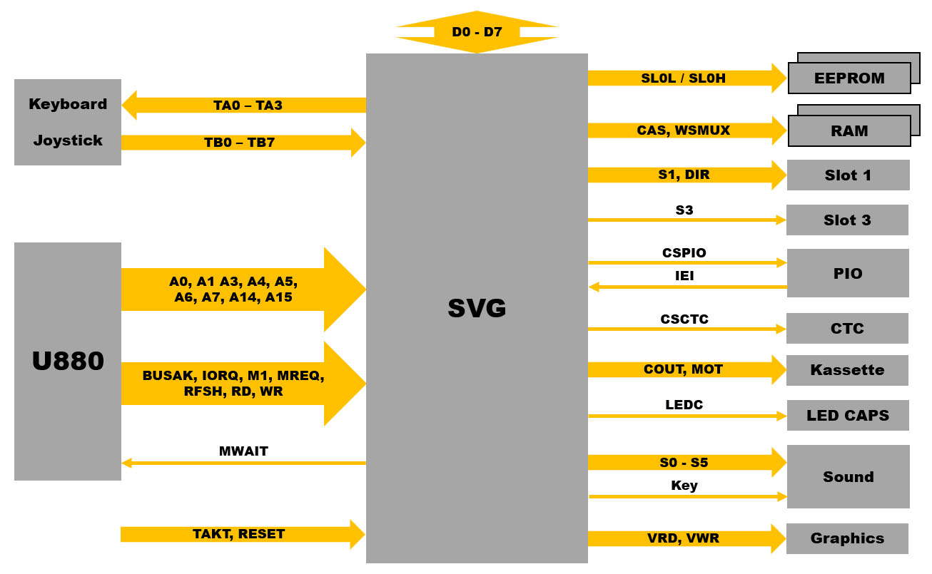
The U1525FC007 is a standard cell ASIC that was used in the Robotron A5105 educational computer. In this part of the documentation, only the structure and properties of the underlying standard cell design system U1520 are considered. A more detailed analysis of the functions of the U1525FC007 is provided in the third part of the documentation. The characters X8 stand for production in August 1989.


The U1525FC007 is based on the U1520 standard cell system. This was a development in the Zentrum für Mikroelektronik Dresden, which later became part of the Carl Zeiss Jena combine. In addition to the U1520 standard cell system, the U1500 standard cell system and the U5200 gate arrays were available. A lot of information on all three systems can be found in the document "Applikative Informationen 4/88" published by VEB Applikationszentrum Elektronik Berlin.

Each of the three architectures has advantages and disadvantages. Simple gate arrays such as the U5200 system contain a fixed arrangement of simple gates and flip-flops. More complex logic blocks are build with combinations of the available gates. To implement the desired functions, only the wiring levels are structured in an application-specific way. This means that the so-called masters can be produced with the same mask set and only a few application-specific masks remain. In the case of the U5200, there are 3 masks.

If you build a circuit with standard cell ASICs such as the U1500 or the U1520, you can use a relatively large number of different standard cells. These gates and flip-flops have a specific, optimized structure. As a result, they require less area and usually have better dynamic behavior. In addition, you can select exactly the number of elements you need and arrange them very freely. However, this also makes the development of such ASICs more complex. Production is also more complex because all masks are application-specific. In the case of the U1500, there are 9 masks. In the case of the U1525, there are 12 masks. What all architectures have in common is that the majority of the structures are known and tested. This simplifies the implementation of an application-specific circuit.

The U1500/U1520 system offers over 40 different standard cells and enables the integration of up to 13.000 transistors. In 1988, a price range of 30-300 Ostmarks was quoted. "Economically favorable quantities" would therefore be 1.000 - 100.000 per year. For the U5200 gate array system, on the other hand, there is an "economic upper limit" of 10.000 units per year.

The standard cell ASICs U1500 and U1520 are based on the CSGT2 process. CSGT stands for "Complementary Silicon Gate Technology". It is a 5V CMOS process with a minimum structure size of 4µm. The operating clock of the process is typically 4MHz, the gate delay is specified as 5ns. Two different variants of the CSGT2 process were used for the U1500 and the U1520. The U1500 is based on the CSGT2/N process, the U1520 on the CSGT2/S process. Although the dynamic parameters of the two processes are different, it is said that neither process can be described as better in this respect. The CSGT2/S just allows higher packing densities because the standard cells are smaller. However, the manufacturing process is more complex.

The successor generations to U1500 and U5200 were the U1600 and U5300 systems, whose minimum structure width is just 1,5µm and which have two metal layers. With even larger chip areas, the maximum possible number of transistors increases to up to 100.000. The operating frequency increases to 25MHz, the gate delay decreases to a maximum of 1,6ns. RAM, ROM and PLA areas were then also available in the U1600 system.


A little earlier, in the document "Applikative Information 3/88", there is a comparison of the advantages and disadvantages of the various product families. ...yeah, german language...  ;)


The picture above shows the rational areas of application in a somewhat simpler way. Standard cell ASICs were considered particularly useful for medium quantities. The range of applications expands towards more complex circuits.


The "Fachbereichstandard" TGL 43876 describes how the standard cell ASICs U1500/U1520 were labeled. Unfortunately, however, the assignment of the description to the characters is slightly off. The designation U1525FC007 is explained as follows: U15 stands for this generation of standard cell ASICs. The 2 shows that the component was manufactured using the CSGT2/S process. The number 5 stands for the maximum chip size with an edge length of 7,5mm. F indicates that it is a ceramic package. The letter C indicates the usual operating temperature range. Finally, 007 is the specific type designation of the ASIC design.


Table 2 of the "Fachbereichstandard" shows which chip sizes were available in the U1500/U1525 system and in which housing types they were available.


The ceramic housing is easy to open.


The picture above shows the die of the U1525FC007 and is available in original size (34MB): https://www.richis-lab.de/images/logic/35x08XL.jpg


There are no inscriptions or symbols on the die. Only on the lower edge are the inscriptions of auxiliary structures visible in the remains of the milling line.


The structure of the U1525FC007 is typical for a standard cell architecture. The active elements are lined up in rows. The cells are connected between the rows via a polysilicon layer for vertical lines and within a metal layer for horizontal lines. The supply voltage is fed in at the side. If circuit parts that are further apart need to be connected to each other, the area between the standard cell rows and the bond frame can be used. This is also where the lines run between the interfaces in the bond frame and the inner circuit parts.

However, the standard cell ASICs did not necessarily have to adhere to this clear architecture. In the U1500PC050, the circuit parts are arranged more individually and have been supplemented with very individual structures: https://www.richis-lab.de/phone03.htm


The document "Applicative Information 4/88" describes how standard cell ASICs were developed. Once the user has defined his logic circuit, the placement and connection of the cells can be done automatically.


According to "Applikative Information 4/88", in the U1500/U1520 system you can choose from a catalog of 43 standard cells. There is a standard cell catalog from which one page is shown. Unfortunately, the complete catalog is not publicly available.

Each standard cell has a name, here "ANO 24". In the top right-hand corner you can see in which process this cell is available. Below this is the associated symbol, the mathematical description and a textual description of the behavior. When designing the layout, the standard cells are represented by rectangles with the respective symbol. The entire layout is divided into grids. The standard cell shown here takes up 7x5 or 8x5 grid cells. The description of the cell shows which interfaces are available at the top and bottom edges.

The gate equivalent makes it possible to estimate the area required for the circuit. A gate is assumed to have four transistors. Accordingly, the ANO 24 gate requires the area of eight transistors.

Finally, the lower section contains the parasitic capacitances of the inputs and the permissible capacitive load of the output. These figures give the maximum permissible number of gates that can be connected to an output. Line capacitances must be added too. The values apply to the typical operating frequency of 4MHz, at lower frequencies, more gates may be connected to an output. The upper limit is 50 gates. The delay of the cell is also defined.


An early standard cell catalog from 1983 is publicly available on the website of Dr. G. Heinz. However, this catalog only documents the possibilities of the U1500 ASICs based on the CSGT2/N process: http://www.gheinz.de/publications/berliner_ics/index.htm#35

The description of the cells is somewhat more detailed in some cases. The first page contains both a circuit diagram and the gate width of the transistors. The second page shows the corresponding structures as found on the die.

This document also states that it was possible to define new standard cells. The new cells must then be agreed with the publishers.


The layout data for the U1520PC201, another U1520 variant, can be found on Dr. G. Heinz's website: http://www.gheinz.de/publications/berliner_ics/index.htm#slic-b

The standard cells are shown as rectangles with the corresponding symbols. The labeled inputs and outputs can be found at the upper and lower edges. The elements have different widths. Flip-flops are slightly higher than standard gates. The necessary input and output blocks are located in the bond frame. Between them, lines in the polysilicon layer and in the metal layer provide the necessary connections.


In the real circuit, the cells are much harder to make out, but with a little practice you can easily recognize the transitions from one cell to the other.


The standard cell catalogue is only available for the CSGT2/N process. Although the CSGT2/S process offers almost the same standard cells, the structures are clearly different. If you know which cells to compare, you can recognise some similarities in a direct comparison. However, this is not sufficient for a simple identification of the cells. For this reason, it is necessary to understand the function of each individual cell. However, knowledge of the basic technology and the logic blocks available is very helpful.


The CSGT2/N standard cell catalog shows the masks used. There are 10 masks listed, but the n+ channel stopper was not necessary, as Dr. G. Heinz explained in detail in 1985: http://www.gheinz.de/publications/berliner_ics/index.htm#18

This results in the 9 masks already described for a relatively simple CMOS process. When looking at the gates, it is immediately apparent that the U1520 is more complex. A second polysilicon layer can be recognized. This matches the 12 customized masks attributed to the U1520 system. This would be a mask to structure the second polysilicon layer. One mask for the contacts to the layer below and one mask for the contacts to the layer above.


The supply lines are located above and below the logic lines in the metal layer. The metal layer (blue) is mainly used for the power supply and signal forwarding between the standard cells. However, it is also partially used within the cells.

The second polysilicon layer added in the CSGT2/S process is only used inside the standard cells (green). It enables the higher integration density and explains the significantly different architecture compared to the U1500. The frame color of the arrows shows on or under which layer the respective layer is located at this point. The visual appearance often changes.

The lower polysilicon layer (pink) is somewhat more finely structured than the upper one. It also represents the gate electrodes. The lower polysilicon layer also provides the contacts to the wiring area. The structures of the polysilicon layers can be seen reasonably well through the metal layer. However, if the edges of the two polysilicon layers cross underneath the metal layer, it is often difficult to identify the conductor routing.

The active areas (white) are located under the other structures. The corresponding edges are clearly visible. At these points, windows have been etched into the thick silicon oxide that otherwise covers the entire wafer ("field oxide"). Transistors only form in these windows when a strip of the lower polysilicon is applied to them.

The active area and the three wiring layers cannot be connected to each other at will. The contacts between the second polysilicon layer and the active area (red) and between the first and second polysilicon layers (orange) are clearly visible. The metal layer can obviously only contact the second polysilicon layer (yellow). If you want to contact the first polysilicon layer or the active area with the metal layer, this must be done via the second polysilicon layer. This sometimes results in contacts that lie on top of each other and areas that appear more complicated than they should be at first glance.


The active areas are always divided into at least two parts. In the upper areas only p-channel MOSFETs are located (red frame). In the lower areas only n-channel MOSFETs can be found (blue frame). The active areas are connected at several points with Vss (blue areas) and Vdd (red areas). In this cell, the Vss contact in the lower left corner is somewhat unclear. This is due to the extended use of the second polysilicon layer. The rectangular contact connects the metal layer with the second polysilicon layer. This then extends to the right and upwards and is connected to two surfaces of the active area via two round contacts.

In the image on the right, the surfaces of the first polysilicon layer are marked in color. Common potentials have the same color. Where the polysilicon covers the active areas, a transistor is formed. The different contact possibilities at the top and bottom edges of the standard cell are clearly visible.

The connections via the second polysilicon layer and the metal layer are marked with dashed lines. Approximately in the middle of the cell there is an area where it is very difficult to assign the contours ("?"). At such points, you have to work with the background knowledge of existing logic functions or record parts of the circuit in order to be able to draw conclusions about the rest.


With the knowledge of the structure and function of the structures, you can finally mark the transistors. Recognizing the circuit is easier than it appears at first glance. Firstly, it is known which logic gates must be present and secondly, the circuits usually only consist of relatively simple parallel and series connections of transistors.

This is an EXOR gate containing five p-channel and five n-channel MOSFETs. The circuit diagram is taken from the standard cell catalog of the U1500. Proper documentation of the standard cells and their contacts is extremely important for further analysis of the circuit.


https://www.richis-lab.de/logic27.htm

 :-/O
« Last Edit: December 23, 2023, 04:25:46 am by Noopy »
 
The following users thanked this post: SeanB, exe, RoGeorge, ch_scr

Offline NoopyTopic starter

  • Super Contributor
  • ***
  • Posts: 1726
  • Country: de
    • Richis-Lab
Re: Logic-ICs - die pictures
« Reply #53 on: December 23, 2023, 04:32:25 am »
I have updated the first part of the U1525FC007:

- I have flipped some of the pictures so we have Vss in the lower areas of the pictures and Vdd in the upper area of the pictures. That is probably more convenient for everybody.

and

- I have added a comparison picture with the layout shown in the CSGT2/N standard.


The upper Post is updated due to hotlinking and editing...  :-/O :)

Offline core

  • Regular Contributor
  • *
  • Posts: 131
  • Country: ro
Re: Logic-ICs - die pictures
« Reply #54 on: December 23, 2023, 06:42:26 am »
I have updated the first part of the U1525FC007:

- I have flipped some of the pictures so we have Vss in the lower areas of the pictures and Vdd in the upper area of the pictures. That is probably more convenient for everybody.

and

- I have added a comparison picture with the layout shown in the CSGT2/N standard.


The upper Post is updated due to hotlinking and editing...  :-/O :)


Very interesting information ! Thanks for sharing.
 
The following users thanked this post: Noopy

Offline NoopyTopic starter

  • Super Contributor
  • ***
  • Posts: 1726
  • Country: de
    • Richis-Lab
Re: Logic-ICs - die pictures
« Reply #55 on: December 26, 2023, 04:47:11 am »


Basis for analysing the standard cells used in the U1525FC007 is the list in the document "Applicative Information 4/88". The relatively old standard cell catalogue for the U1500 represents only a subset of the available cells, but it is helpful because it also contains the circuitry of the respective cells. In the U1525FC007, 21 different gate types and 3 interface blocks were used.


The negator or inverter, NEG1, is the simplest gate. It merely inverts the input signal. This behaviour is self-evident if the input signal is used to control a push-pull stage consisting of a p-channel MOSFET (red) and an n-channel MOSFET (blue).

As only two transistors are required, the corresponding cell on the die is very narrow. The input signal contacts a polysilicon strip that runs across two active areas. On the right, these are connected to the supply potentials. On the left-hand side, the second polysilicon layer contacts both transistors and the output signal generated there is led out upwards and downwards. A small metal contact would also make it possible to tap the output signal in the cell via the metal layer. Such metal contacts, which could be used to connect the various gates, can be found in many standard cells. However, they are never used in the U1525FC007.

In his 1985 lecture, Dr G. Heinz explains that in the CSGT2/N process, a connection between the polysilicon and the active area is only possible via a metal island. (http://www.gheinz.de/publications/berliner_ics/index.htm#18) Of course, this could also have been the case with the CSGT2/S process of the U1525-FC007 and would then be an explanation for the unused metal contacts. However, the circuits and the associated layouts show that, as described, the metal layer can contact the upper polysilicon layer and the upper polysilicon layer then contacts the lower polysilicon layer or the active area.


The clocked inverter bears the abbreviation NGT. It is an inverter that is extended upwards and downwards with additional transistors. The additional transistors use the clock signal to control the forwarding of the signal. Like most clock-controlled gates, the clocked inverter also requires a complementary clock signal in addition to the clock signal.

The real implementation is more complex, but still clear. Here too, the output signal is also applied to a small metal island located in the centre of the cell.


The TRIS cell is an auxiliary circuit that is used to control outputs that also enable a tristate state. It is a combination of an inverter, a NAND and a NOR gate. If a high is present at control input Z, output AP remains high and output AN remains low regardless of the status at signal input E. Otherwise, the outputs pass on the current level of the signal input. In this cell, the metal layer is used more often, which makes it much more confusing.


In the ANO24 cell, two AND gates are combined with an OR gate. Here too, the output potential is additionally connected to a metal island within the cell.


In the ANO4 cell, an AND and an OR gate are combined with a NOR gate.


The NAND gates NA2, NA3, NA4 and NA6 are very clearly structured. The variant with six inputs is only available for the NAND gates, not for the NOR gates.


An EXOR gate requires a relatively large number of transistors compared to a NOR gate.


The ONA24 provides the user with a further gate combination. In this case, there are two OR gates that are combined via a NAND gate.


The ONA3 is a simpler gate combination. This is an OR gate that is surrounded by a NAND gate.


Like the NAND gates, the NOR gates are very clear.


The ES block is a simple input that behaves like an inverter. With the ESH and ESL blocks, there are additional inputs that also forward a defined signal in the unconnected state.

There is a protection circuit at the bondpad, consisting of a diode to the Vdd potential and a diode to the Vss potential (pink/green). A strip of the active area forms a resistor that serves as a current limiter (yellow).

On the right are the p-channel and n-channel MOSFETs, which act as inverters for the input buffer. It is interesting to note that the n-channel MOSFET is twice as large as the p-channel MOSFET. This is unusual. The p-channel MOSFET is usually larger because it has poorer properties.


The simple push-pull output is labelled AS1. To the right and left of the bondpad is a whole row of p-channel and n-channel MOSFETs, which can provide the necessary current delivery capability.


The BDL interface is bidirectional and offers a tristate state. For this purpose, the gates of the large output transistors are led out individually. They are usually controlled via the TRIS cell.

A line also leads from the bondpad to the input circuit in the upper area. The familiar protective structures are integrated on the right and left. The transistors of the buffer inverter are located between them. Here too, the n-channel MOSFET is surprisingly large. The L stands for the fact that the block outputs a low level when the input is not connected. An additional p-channel MOSFET is integrated for this purpose, whose gate is connected to the Vss potential and thus represents a pull-up resistor at the input.


The DFFR cell is a master-slave D flip-flop with reset input. The circuit consists of 12 p-channel and 12 n-channel MOSFETs and occupies a correspondingly large area. All master-slave flip-flops are slightly higher than the normal gates to enable a sensible arrangement of the elements.

Here, both the output signal and the complementary output signal, as well as the clock signal and the complementary clock signal can be contacted via the metal layer in the centre of the cell. The lines were also routed to the side edges, presumably to enable simple cascading. These contacts were never used in the U1525FC007.


The master-slave D flip-flop with set and reset input, DFFRS, is the largest standard cell found in the U1525FC007. The circuit does not quite correspond to the circuit diagram. However, the differences are hardly relevant. As in the DFFR cell, the transistors connected to the clock signal are located on the outside, near the supply potentials.


The master-slave D flip-flop with set input, DFFS, is very similar to the DFFR cell.


The LFF cell is a simple D flip-flop. In contrast to the master-slave flip-flops, the normal cell height is sufficient here.


A simple D flip-flop with set input is also available under the designation LFFS.


The RSNA cell is an RS flip-flop. It is an interconnection of two NA2 gates.


Some of the standard cells have been additionally mirrored.


The U1525FC007 contains 1.001 gates using a total of 6.902 transistors. Excluding the gates in the bond frame, 935 gates were used.


https://www.richis-lab.de/logic28.htm

 :-/O
 
The following users thanked this post: SeanB, RoGeorge, ch_scr

Offline NoopyTopic starter

  • Super Contributor
  • ***
  • Posts: 1726
  • Country: de
    • Richis-Lab
Re: Logic-ICs - die pictures
« Reply #56 on: December 29, 2023, 04:19:49 am »


There is no datasheet for the U1525FC007. The module was specially developed for the Robotron A5105 educational computer. A circuit diagram of this computer system can be found on Ulrich Zander's website: https://www.sax.de/~zander/bic/bic_hw.html This allows you to recognise the approximate functionality of the pins and the circuit.


The freeware Inkscape is ideal for analysing the U1525FC007. It allows you to conveniently place and manage a large number of symbols and texts on the die.


In the first step, the bondpads are labelled with the pin designations from the circuit diagram.


In the second part of the documentation, all gate types were identified. Ideally, all gates should be marked on the die in this step. Here, a square was placed around each gate. Inkscape links a consecutive number to the square. The different colours stand for different gate types. If you create folders for the different gate types, this will make it easier to find them later.


The next step is to mark all signals that arrive at the U1525FC007 or are transmitted to the outside. Different colours and collective folders also provide a better overview here. This preparatory step is not absolutely necessary, but it makes it easier to analyse the circuit further.

Prominent signals can be marked one or two levels deeper in the circuit. For example, the reset signal passes through several inverters, partly to distribute the capacitive load of the many receiver gates and partly to generate an inverted signal. The display of a double inversion appears unnecessary at first glance, but indicates that this signal is slightly delayed compared to the original signal.


The die marked in this way serves as the basis for further analysis of the circuit.


Various programmes can be used to document the circuit. KiCad was used here. KiCad is actually used to create circuit board layouts. I think everybody here knows it.  ;) However, the circuit diagram editor is also suitable for documenting logic circuits. The 24 standard cells of the U1525FC007 must first be added to the component library.

Minor peculiarities, such as the descending numbering of the inputs on the NOR gates, resulted from initial errors in the analysis, which only became apparent after the circuit diagram was created. In order to keep the change effort within reasonable limits, such cosmetic peculiarities were accepted.


KiCad numbers the gates automatically. This designation is used in Inkscape as the name for the corresponding rectangle. This allows you to find a gate in Inkscape later. It is also easy to see which gates have already been included in KiCad. In addition you can fill the rectangles with 50% transparency black. This makes it easier to analyse because you can immediately see whether a line leads to a known gate.

The fully marked SVG file is stored here (174MB): https://www.richis-lab.de/images/logic/35x57.svg


The circuit is best recorded from interfaces whose downstream functions are known or at least can be surmised. If, after a certain amount of time, you can't get a feeling for how the local part of the circuit is developing, you should switch to another part of the circuit. When documenting the circuit, you will gradually gain an understanding of how it works and you can arrange and group the gates in KiCad in a sensible way.


https://www.richis-lab.de/logic29.htm

 :-/O
 
The following users thanked this post: SeanB, RoGeorge, ch_scr

Offline NoopyTopic starter

  • Super Contributor
  • ***
  • Posts: 1726
  • Country: de
    • Richis-Lab
Re: Logic-ICs - die pictures
« Reply #57 on: January 02, 2024, 10:13:54 am »


The interfaces of the U1525FC007 can be extracted from the circuit diagram of the Robotron A5105 educational computer. The module is connected to the 8Bit wide data bus and receives the clock signal and the reset signal, which is also used by the processor. The processor is a U880, which is functionally equivalent to a Z80. The U1525FC007 receives some control signals directly from the processor, from which it generates the MWAIT signal, among other signals. Nine address lines are processed from the 16-bit wide address bus. The module checks the keyboard or joysticks and generates the sound. The U1525FC007 also supports the U880 in the selection of various function groups: ROM, RAM, optional plug-in cards, PIO and CTC module, graphics unit and an optional cassette drive.
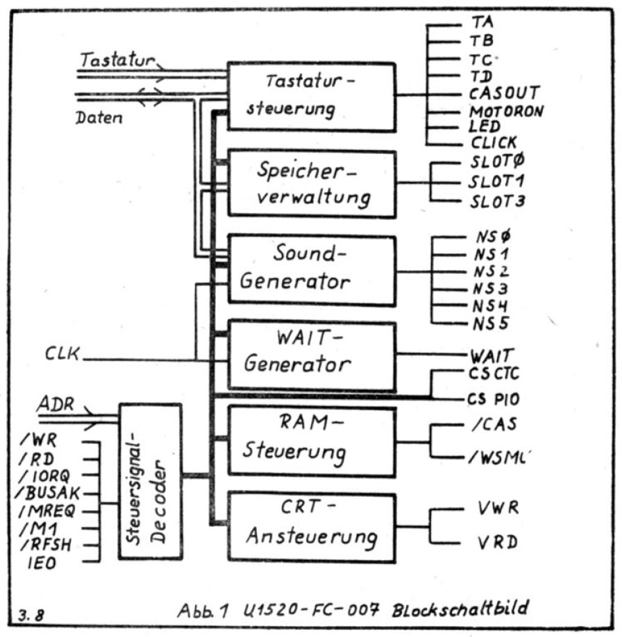


The papers presented at the 13th Microelectronic Components Symposium (Volume 7) contain some information on the U1525FC007. There the designation U1520-FC-007 is used, in which the chip size is missing. In addition to the abbreviation SVG, the component is also described as a "circuit for memory management and sound generation". The printed block diagram matches the integration in the Robotron A5105.
Like the Z80, the U880 can control a maximum memory volume of 64kB. The U1525FC007 extends the address table. The Robotron A5105 contains two EPROMs with a volume of 32kB and 8kB. There are also two DRAM modules, each with 32kB. The memory can be expanded using plug-in cards. The Microelectronic Components Symposium mentions 256kB of RAM. It is more plausible that the memory area can be expanded to a total of 256kB. The RAM may then be a maximum of 192kB in the A5105.
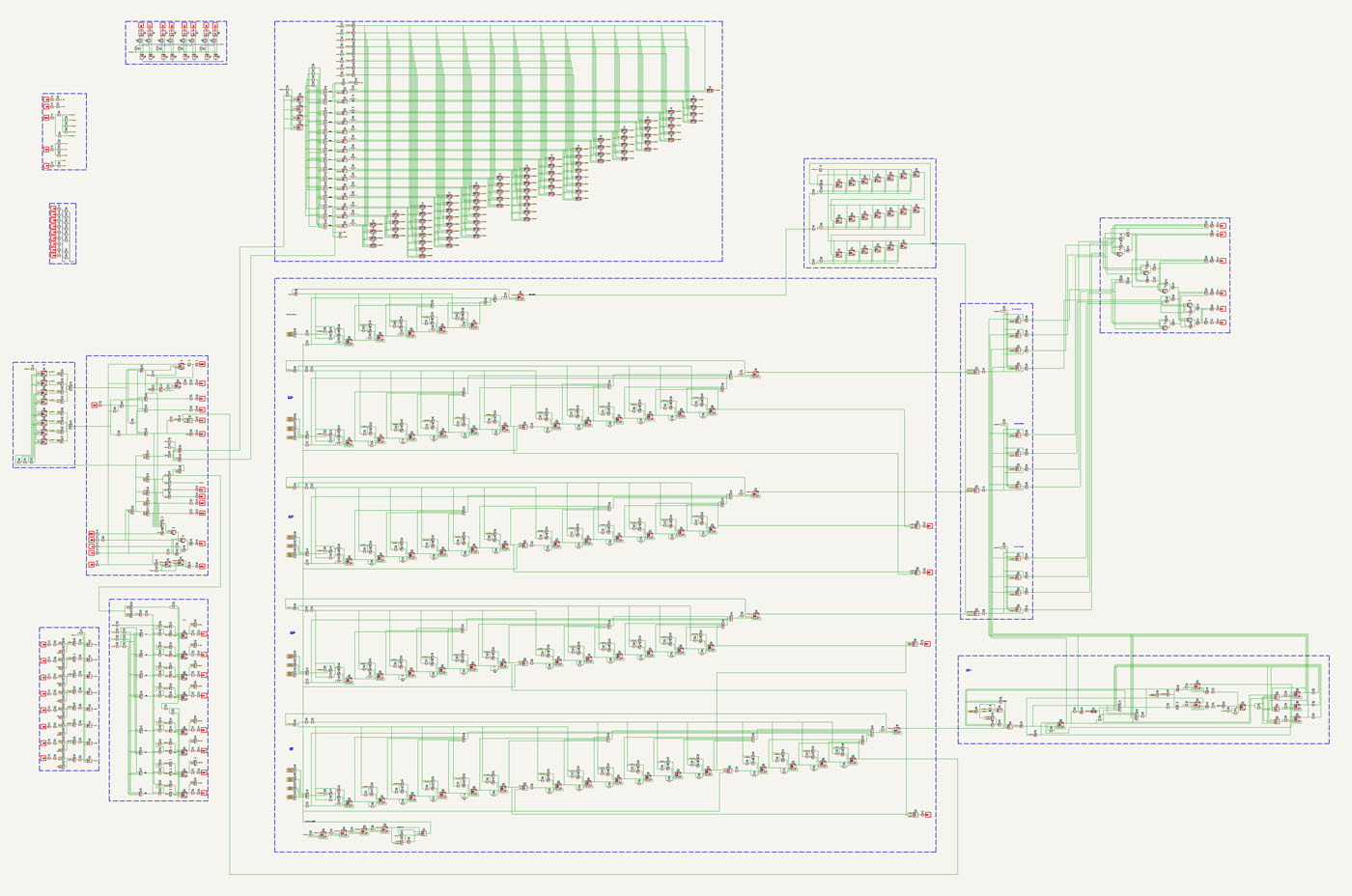


The logic in the U1525FC007 has been completely transferred to a KiCad circuit diagram. The use of only one sheet simplifies the creation of the logic circuit, as you can work more creatively. In addition, there are very large circuit blocks, the division of which would have an unfavourable effect on clarity. The thick blue frames represent a demarcation of self-contained function blocks. The block diagram from the 13th Microelectronic Components Symposium was not yet available here, which is why the layout of the circuit is not based on it. However, the block diagram is fully consistent with the extracted functions.
The KiCad file can be downloaded here: https://www.richis-lab.de/images/35x64.kicad_sch (2MB). Such large graphics cannot be packed into common image formats such as JPEG. An SVG file is available here: https://www.richis-lab.de/images/35x83.svg (14MB). It can be opened and edited in Inkscape.
The following relationships and functions have been extracted and documented as good as possible. However, it is quite possible that minor errors have crept in, individual addresses are not quite correct or potentials have been inverted.
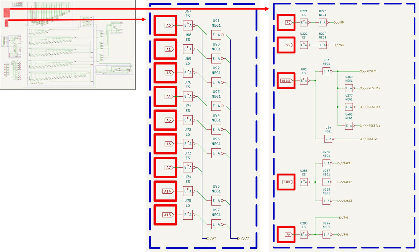


Some interfaces can be used as a starting point for the documentation of the circuit. These include the address bus, for example. The global identifiers outlined in red are the interfaces to the outside, i.e. the bondpads. Internally, most connections are shown as continuous lines. Only some highly branched potentials, such as the address bus, are distributed on the circuit diagram with so-called hierarchical identifiers. The address bus first passes through the input gates. Most address lines are also inverted for further use.
Further global signals are collected on the right, for example the read and write signals. The reset signal serves a total of 55 gates. The large number is probably one reason why five inverters pre-process the signal. The clock signal only serves seven gates, yet three inverters have been integrated here. The requirements for signal integrity were probably higher than for other signals. In the Robotron A5105, the PM potential is connected to the 5V potential via a pull-up resistor. The function of this potential will be considered in more detail later.
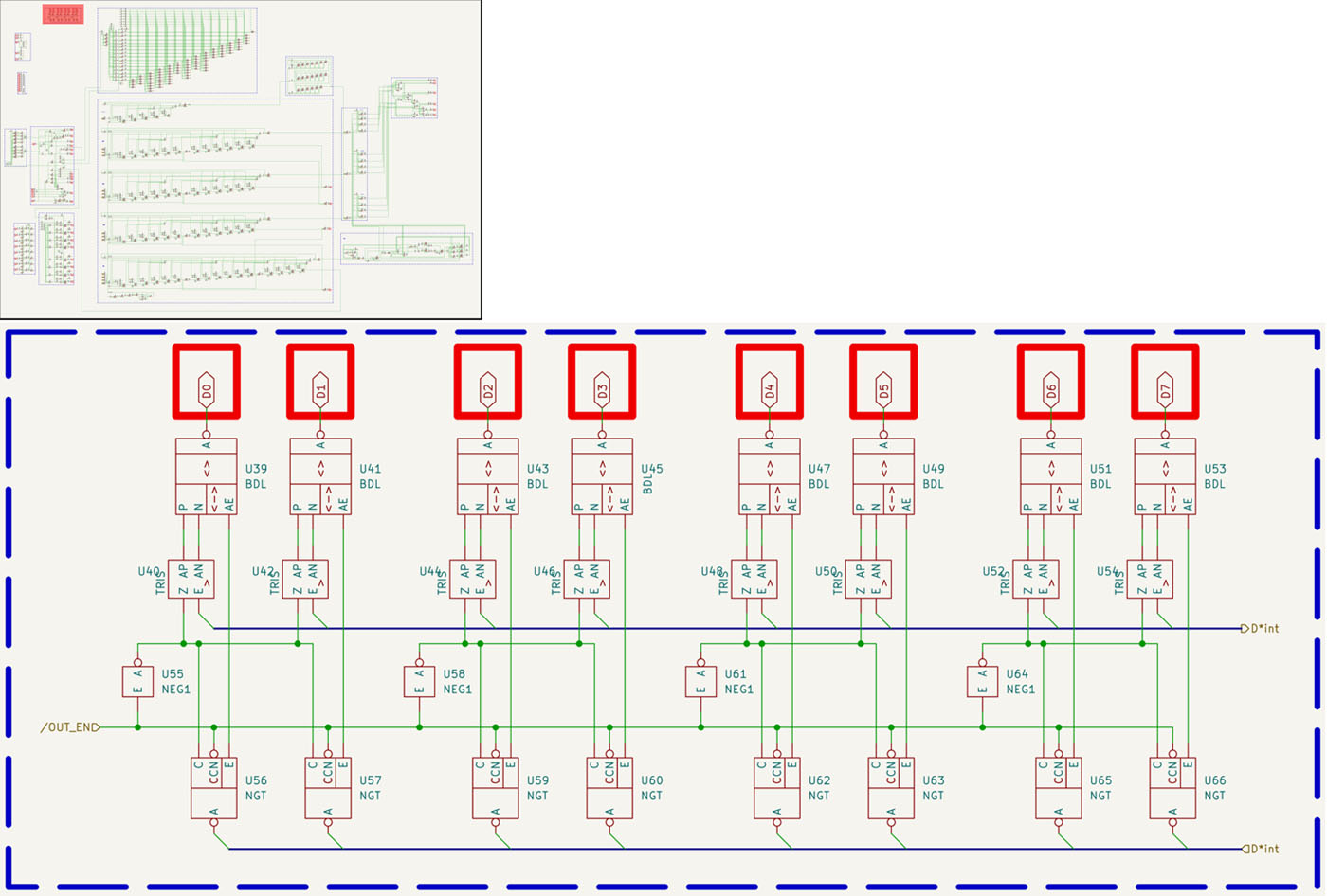


The data bus is routed to bidirectional interface gates with tristate function. These interface gates are controlled via TRIS gates. The /OUT_EN signal controls whether data may be placed on the data bus or whether the current potentials are to be read in. Clocked inverters are used to read in the data. An internal data bus is generated from this circuit.


A function block controls the addressing of the memory areas. SL0L and SL0H each activate one of the two EPROM modules. S1 and S3 can be used to select the two interfaces for optional modules. The selection of the two 32kB RAM modules is controlled via CAS and WSMUX. Everything is controlled via the internal control signals S1 and S2.
The second function block generates a whole series of control signals based on the address lines and the control signals of the U880. In addition, the interrupt output of the PIO module is analysed. The read and write signals for the graphics unit, which also serve as selection signals, are output directly. The selection signals for PIO and CTC are also output directly. The DIR signal defines the flow direction of the data transceiver at the connectors for the optional modules. The WAIT signal is used to signal to the processor when the addressed resource is available.
The right-hand function block also generates some internal control signals. One of these enables data to be transferred to the data bus. Further control signals can be used to transfer data to the internal registers. In the presentation from the Microelectronic Components Symposium, two of the registers are labelled Port A and Port C. Port A is written in parallel. Port C can be written in parallel or serially via two control signals. The integrated sound generator has very extensive configuration options. The register to be written to is selected via a control signal. A second control signal can then be used to write to this register.


The control signals SL0L, SL0H, SL1, SL3, WSMUX and CAS are selected by linking the internal control signals S1 and S2 with the control signals of the processor. S0L and SL0H are also dependent on address bit A15.
WSMUX and CAS also have flip-flops which ensure that the address of the processor is split into row and column selection. If MRQ is active, the RAM immediately takes half of the address as row selection. If the RAM is selected, the circuit in the U1525FC007 ensures that the second half of the address is switched through to the RAM with WSMUX and this part is subsequently adopted as column address with CAS.
At first glance, it seems strange that the row selection in the RAM always takes place, even if the RAM is not selected at all. This transparency is necessary so that the DRAM can be refreshed, which the U880, like the Z80, carries out automatically. As the DRAM only outputs data on the bus with a column address, the selection of a row address alone does not lead to a bus collision.


The decoding of the control signals is quite clear. The links between the addresses and the control signals can be easily extracted. While MRQ indicates an access to the memory area, the processor uses IORQ to communicate an access to a peripheral circuit. The signal M1 belongs to such an interrupt cycle.


The generation of the DIR and MWAIT signals can be seen here. The U1525FC007 only inserts a fixed delay between the start of a memory interaction and the positive feedback via MWAIT.


The Port A register can be used to configure the addressing of the memory areas. The current value of the data bus is saved in port A with the corresponding control signal. The stored value can also be read out.
Depending on which of the eight bits are set in port A, different combinations of address bits 14 and 15 are required to activate the control signals S1 and S2. Various combinations do not make sense. In all probability, only two bits are ever set in port A. Combinations that activate S1 and S2 with the same address combination also appear to make little sense and are painted grey here.


The Port A register is build with DFFR flip-flops.


To be able to select a memory area, RFSH must have a high level and MRQ a low level. This means that there is no refresh cycle active and the processor wants to access a memory. The control signal combinations 01 and 11 can be used to select the interfaces of the optional plug-in cards (SL1/SL3). 10 activates WSMUX / CAS and thus the interface of the RAM modules.
SL0L and SL0H, the two EPROM modules, are only active if no bit is set in the Port A register. This appears illogical at first glance, as no other memory area can be activated in this state. Port A must first be rewritten. However, this implementation has the advantage that the EPROMs where the program is located can be accessed immediately after a reset without initialising the SVG. By linking to address bit 15, the control of the EPROM initially appears completely transparent to the processor.


A multiplexer makes it possible to place various data on the data bus. One data source is the TB* inputs, which show the processor which key on the keyboard is pressed. Alternatively, the data in the Port A or Port C registers can be placed on the data bus. One of the three data sources is selected via the address lines A0 and A1.
The data register Port C can be loaded with data in parallel or serially. The content of the register controls the line selection of the keyboard logic (TA*), the cassette recorder, the caps lock LED and the signal for the key tone.


Here you can see a part of the multiplexer.


The Port C register is constructed with DFFRS flip-flops. The register can be loaded in parallel via the D inputs. Serial loading takes place via the set and reset inputs. The underlying logic evaluates the level of data bit 0. Data bits 1 to 3 define which bit of the register is to be written.


The sound generator takes up a lot of space in the U1525FC007. The configuration registers account for a large proportion of this. There are 16 registers with a total of 83 bits.
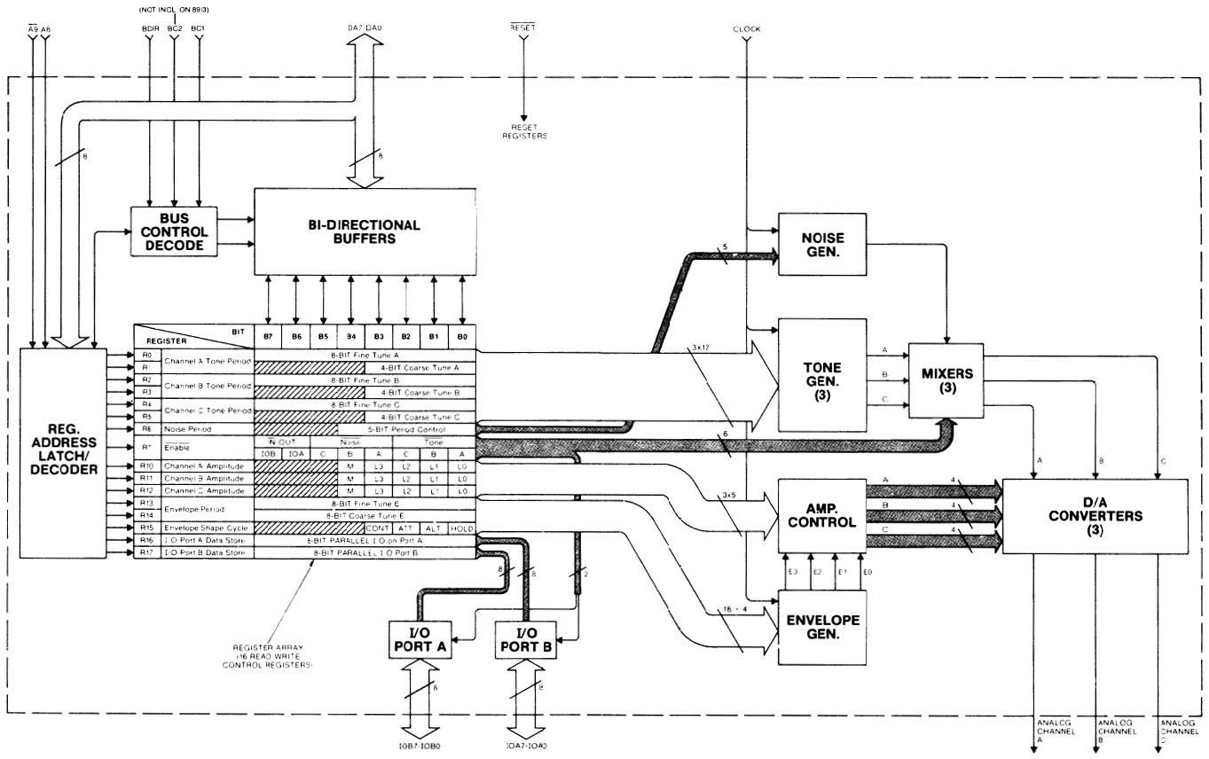


The sound generator integrated in the U1525FC007 is very similarly to the AY-3-8910 sound generator from General Instrument. Even the control registers have the same structure and arrangement. The U1525FC007 only lacks the Port A and Port B interfaces and the mixer at the output mixes the signals into a single channel. In addition, the digital-to-analogue converter is located externally.
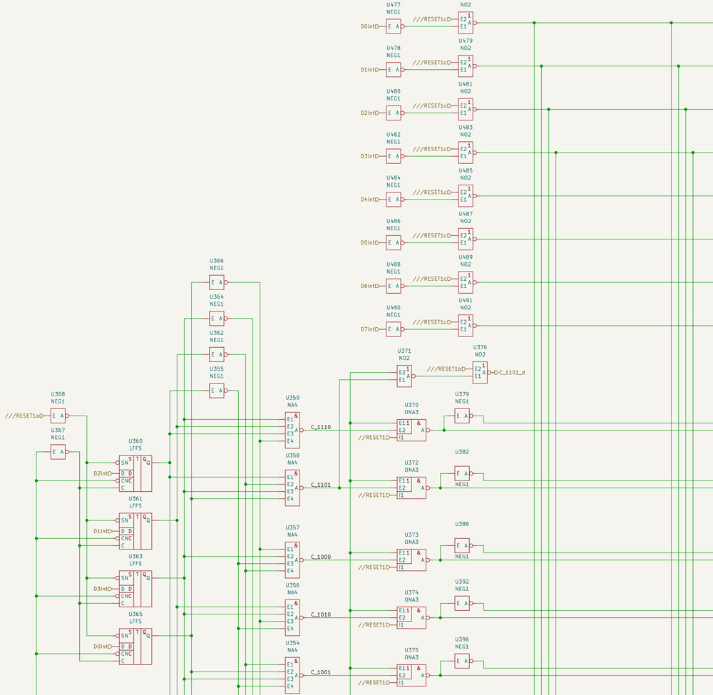


Four LFFS flip-flops use the first four bits of the data bus to select a line of the configuration register for the sound generator.
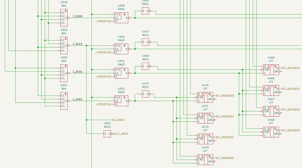


With some additional logic, the LFFS flip-flops generate the clock signals for LFF flip-flops, which represent the configuration registers themselves. The inputs are connected to the data bus. One address triggers the LFFS flip-flops and thus the line selection. Another address then allows the LFF flip-flops to accept the data on the data bus.
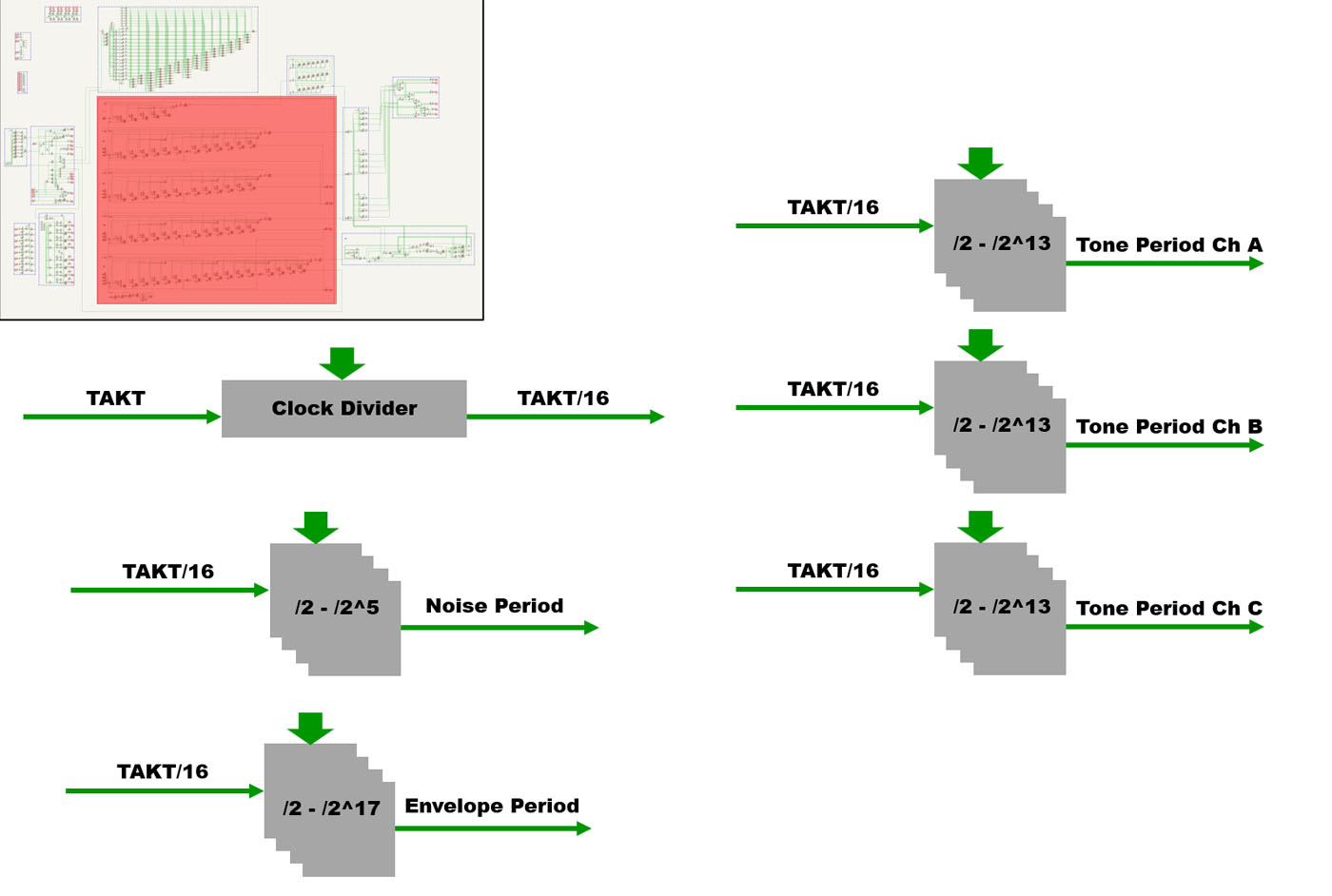


The sound generator is based on six clock dividers. The 3,75 MHz basic clock of the A5105 can first be divided down by a factor of 16 before it is then passed to the five other clock dividers as a working clock.
One clock divider defines the basic frequency of the noise generator and can divide the working clock by 2 to 2^5. A further clock divider generates the clock for the amplitude modulation with a divider factor of 2 to 2^17. The three tones that the sound generator can supply are generated via three clock dividers, each with a divider factor of 2 to 2^13. This results in a frequency range from 28Hz to 117kHz.


The clock dividers are based on DFFRS flip-flops. Their exact mode of operation only becomes apparent at second glance. The circuit not only takes up a lot of space on the circuit diagram, but also on the die.
The interfaces PM, OP0, OP1, OP2 and OP3 appear to be used for diagnostic purposes. The frequency dividers of channels A, B, C and the envelope generator are divided into groups of six and one group of four. This results in nine groups that can be read out individually. The selection signal for register 0010 switches the four OP outputs, making it possible to reach eight of the nine groups. The PM input can be used to isolate the groups from each other and feed them with the same clock signal. The PM signal also switches the remaining group to the S0H output.


The sound generator contains a noise generator that also uses a divided clock frequency.


Of course, this is only a pseudo-noise generator that does not really generate random noise. There are 20 DFFS flip-flops connected in series. The input signal is generated by an EXOR gate, which links the current output signal with the output signal of the third flip-flop. This results in a pseudo-random output signal.


The envelope, i.e. the amplitude modulation of the output signal, can be defined with a further circuit section. The basis here is also the divided working clock.


The datasheet of the AY-3-8910 shows which envelopes can be generated. The circuit itself is rather confusing. It feeds four data lines, the value of which represents the current amplitude.


The configuration register ultimately defines which of the three tones is forwarded. Each tone can be linked to the noise signal or just the noise signal can be forwarded. The three signals then pass through an amplitude control, which can be set via the configuration register and is also modulated with the generated envelope function.
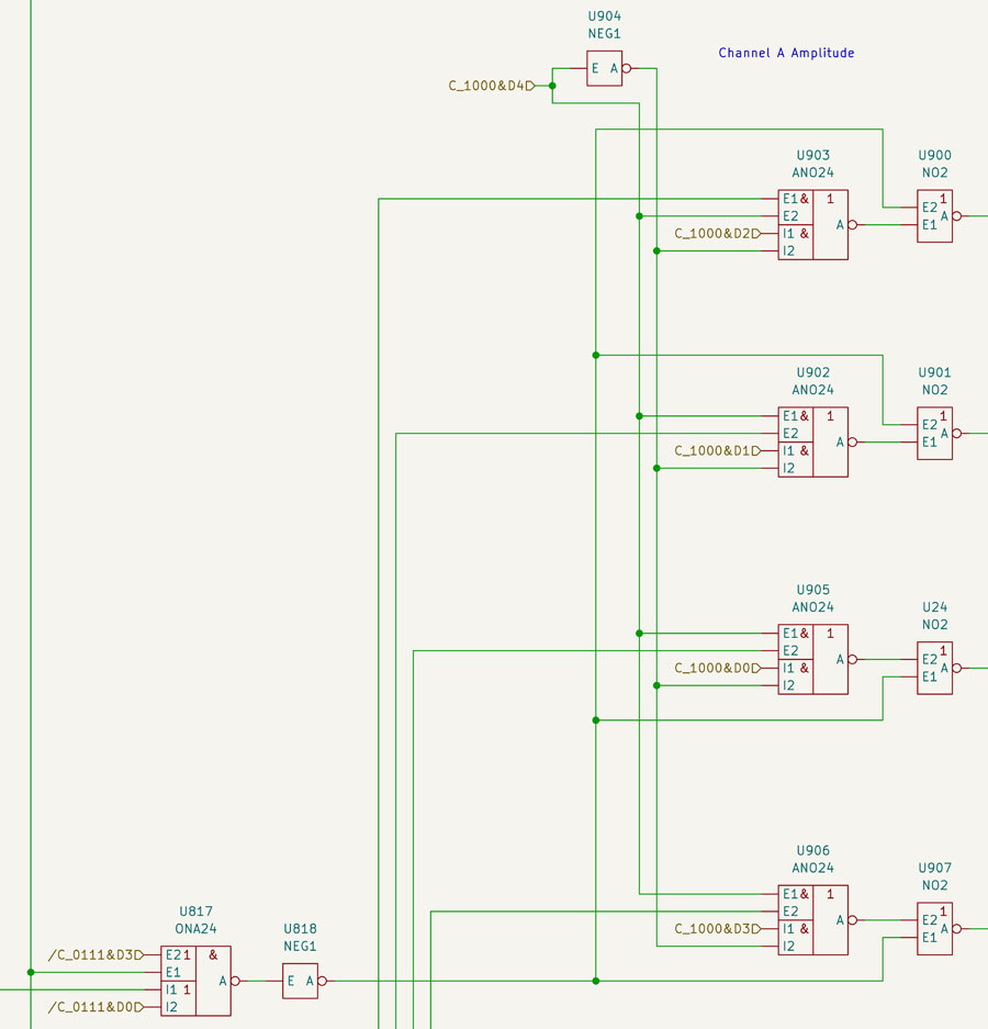


Here you can see the circuit for one channel. The tone or the noise signal or both signals are selected in gate U817. The NOR gates on the far right pass on the signal if the ANO24 gates in front of them allow this. The amplitude configuration and the envelope information are linked in these gates. The four outputs all carry the same signals when they are active. Depending on which of the outputs are active, different amplitudes will result later.


The functionality of the sound output becomes clearer if you take a look at the circuit diagram of the A5105. There, a resistor chain represents a discrete DAC. Each S output serves an inverter, which influences the output level more or less depending on the connection point.


Before the sound signal is delivered, a mixer combines the three generated channels.


https://www.richis-lab.de/logic30.htm

 :-/O
 
The following users thanked this post: SeanB, RoGeorge, ch_scr

Online iMo

  • Super Contributor
  • ***
  • Posts: 4750
  • Country: nr
  • It's important to try new things..
Re: Logic-ICs - die pictures
« Reply #58 on: January 26, 2024, 08:52:49 am »
 

Offline NoopyTopic starter

  • Super Contributor
  • ***
  • Posts: 1726
  • Country: de
    • Richis-Lab
Re: Logic-ICs - die pictures
« Reply #59 on: January 26, 2024, 02:55:18 pm »
Yeah, that´s cool. I have an old and very special HP die here and thought it was SoS too. It had a strange colour but unfortunately it´s not SoS.  :(


Share me

Digg  Facebook  SlashDot  Delicious  Technorati  Twitter  Google  Yahoo
Smf