Author Topic: Logic-ICs - die pictures  (Read 13258 times)

0 Members and 1 Guest are viewing this topic.

Online NoopyTopic starter

  • Super Contributor
  • ***
  • Posts: 1725
  • Country: de
    • Richis-Lab
Logic-ICs - die pictures
« on: January 25, 2021, 09:34:49 pm »
Let´s take a look into some logic ICs.
You can find an overview here: https://www.richis-lab.de/logic.htm


First logic IC is a CPLD, a Lattice ispLSI1016.
The LSI1016 is the smallest CPLD of this model range. The isp variant can be programmed in circuit.
16 logic blocks, 2000 gates, 96 register, 36 I/Os, max 80MHz, max delay 15ns


The die is quite big: 6,1mm x 4,1mm
The datasheet states that the ispLSI1016 was manufactured with a 0,8µm process. Challanging my capabilities.  :-/O ;D


A 1992 design.


A first revision?
Quite a lot of masks.


In the dicing area there are quite some symbols and test structures.


Developer initials?  :-//


Here you can see an I/O bondpad. On the top of the bondpad there is the input structure. At the left and the right sides of the bondpad there are the Push-Pull-transistors.


Here you can see an input stage. I assume the big structures are clamping diodes. Behind the clamping diodes there is a small resistor and a transistor probably acting as a pull-up or pull-down.


The structures are quite small but you can identify the big functional blocks.


There are a lot of small structures between the bondpads which probably do some housekeeping.
Here you can see one of the more interesting circuits. Perhaps a small memory? Perhaps a multiplexer for connecting the distributed memory cells?


Global logic block and I/O cell. Between the two you can spot the 16 lines of the output routing pool.
(Quite likely, you can´t be 100% sure.)


Global logic block input logic array.


Global routing pool, in there are quite a lot of interconnections with their memory cells.


More pictures here:
https://www.richis-lab.de/logic01.htm

 :-/O
 
The following users thanked this post: SeanB, edavid, RoGeorge, Miyuki, jxjbsd

Online ataradov

  • Super Contributor
  • ***
  • Posts: 11234
  • Country: us
    • Personal site
Re: Logic-ICs - die pictures
« Reply #1 on: January 25, 2021, 09:49:49 pm »
SJDC - San Jose Design Center.
Alex
 
The following users thanked this post: Noopy

Offline RoGeorge

  • Super Contributor
  • ***
  • Posts: 6174
  • Country: ro
Re: Logic-ICs - die pictures
« Reply #2 on: January 25, 2021, 10:27:20 pm »
Thank you, subscribed!   :popcorn:

Offline exe

  • Supporter
  • ****
  • Posts: 2562
  • Country: nl
  • self-educated hobbyist
Re: Logic-ICs - die pictures
« Reply #3 on: January 26, 2021, 05:55:59 pm »
A first revision?
Quite a lot of masks.

So, masks are used to amend errors on photo templates?
 

Online ataradov

  • Super Contributor
  • ***
  • Posts: 11234
  • Country: us
    • Personal site
Re: Logic-ICs - die pictures
« Reply #4 on: January 26, 2021, 06:01:38 pm »
No, by "masks" he meant the photo template. That's how they are called in the industry.

Each test structure represents one mask. And this is a lot indeed. But configurable devices are complex in their design.
Alex
 

Online NoopyTopic starter

  • Super Contributor
  • ***
  • Posts: 1725
  • Country: de
    • Richis-Lab
Re: Logic-ICs - die pictures
« Reply #5 on: February 23, 2021, 01:36:37 pm »


D146, a BCD/7-segment decoder built by HFO.


3,0mm x 1,8mm


Test-transistor...  :-/O


The SN7446 datasheet contains a logical schematic (Texas Instruments, 1988).


Well we find everything shown in the shematic.
The two input gates at the inputs A-D are marked in pink. The purple squares are the output transistors of the eight gates.
Between the inputs you see the lamptest circuit (green) and the blanking circuit (black).
The outputs of the input gates are connected to the decoder matrix (dark green) containing both, the connection matrix and the AND-gates. The big gate of the blanking circuit is placed in this area too. The blue parts are the pull-up-resistors for the decoder.
On top of the decode area there are seven NOR-gates with two or three inputs (orange). There are yellow pull-up-resistors and the last parts are the output transistors (red).


Here you can see the input gates.
The first gates are built with an input stage (buffer or AND), a phase splitter and an output lowside transistor. There is no highside transistor but there is a diode connecting the pull-up-resistor of the phase splitter to the output. In the second gates they spared the phase splitter.
The input of the gates are built with transistors with big base areas in which there are one (buffer) or two (AND) emitter areas forming the inputs. The buried collector is the output of the gate input stage.


In the middle of the die there is the decoder containing 19 multi emitter transistors.


The upper contact is connected to the collector. The lower contact is connected to the base area. In the base area there are some emitters connected to the outputs of the input gates.
There is one rotated transistor. That´s the big gate for the blanking of the 0. This gate works with the same input signals so it was reasonable to place the gate in this area.


You can spot every logical connection formed with a emitter and its contact.
But what´s that? There is an additional connection not shown in the SN7445 datasheet: B1/a2


With this connection you get two more segments.
In my view that 6 looks better.  ;D


Here you see the seven NOR-gates and the output transistors.


Nothing special...
There is an substrate connection at every transistor to prevent ground bouncing in the die.


https://www.richis-lab.de/logic02.htm

 :-/O
 
The following users thanked this post: SeanB, ebclr, doktor pyta, RoGeorge

Online NoopyTopic starter

  • Super Contributor
  • ***
  • Posts: 1725
  • Country: de
    • Richis-Lab
Re: Logic-ICs - die pictures
« Reply #6 on: February 23, 2021, 05:15:26 pm »
Minor corrections:


Compared to the 7446 there are two additional connections (yellow).


Symbol 6 and symbol 9 are different to the 7446. Symbol 12 is not different.


=> The D146 is more like a 74246 not like a 7446.  :-+

 
The following users thanked this post: exe

Online NoopyTopic starter

  • Super Contributor
  • ***
  • Posts: 1725
  • Country: de
    • Richis-Lab
Re: Logic-ICs - die pictures
« Reply #7 on: March 14, 2021, 09:27:22 pm »


Now let´s take a look into a ispLSI1024.


The LSI1024 has one megablock more than the LSI1016.


The die is 6,5mm x 5,8mm.


A lot of test structures.


There are also some more complex structures in the slicing area.


The LSI1024 was designed in 1991 while the LSI1016 was designed in 1992 (perhaps the second revision?).


HD24-00, the first revision of the "HD24"?


Push/Pull-Transistors and input protection at the bondpads.


...
A lot of small circuits are placed in the bondpad area.


The LSI1024 is quite similar to the LSI1016 but here we have a third megablock. Since the third megablock is cut in two pieces they needed an additional connection line in the upper area.


Let´s take a look into one of the eight segments of the megablock.


Here there should be two I/O cells.


Global-Logic-Block


Global-Logic-Block connection array


Global-Routing-Pool


Some more pictures:

https://www.richis-lab.de/logic03.htm

 :-/O
 
The following users thanked this post: SeanB, daqq, RoGeorge, Miyuki

Offline aheid

  • Regular Contributor
  • *
  • Posts: 245
  • Country: no
Re: Logic-ICs - die pictures
« Reply #8 on: March 15, 2021, 02:13:16 am »
Love your threads, excellent stuff! Very interesting to look under the bonnet, so to speak.
 

Online NoopyTopic starter

  • Super Contributor
  • ***
  • Posts: 1725
  • Country: de
    • Richis-Lab
Re: Logic-ICs - die pictures
« Reply #9 on: March 15, 2021, 04:08:37 am »
Thanks for the positive feedback!  :-+ That keeps me taking more pictures.  8)

Online NoopyTopic starter

  • Super Contributor
  • ***
  • Posts: 1725
  • Country: de
    • Richis-Lab
Re: Logic-ICs - die pictures
« Reply #10 on: April 11, 2021, 09:23:58 pm »
I have some different controller periphery chips. Will post them here.


Mitsubishi M5L8288, a bus controller for a 8086 processor.


Two bondwires for the supply. The seven command outputs can sink more than 220mA. That is not too much for one bondwire but the voltage drop can cause switching problems.


Mitsubishi used two metal layers.


The name of the design?


Some symbols to check the production quality.


Around the die the two metal layers distribute the supply voltage.


The command outputs. Between the bondpads there are the big lowside transistors. On the left side of the bondpads there are the smaller highside transistors.
Wide metal stripes supply the outputs.


Here we have one of the weaker outputs. The lowside transistor (right of the bondpad) is bigger than the highside transistor (above the bondpad) but both are smaller than the transistors of the command outputs.


https://www.richis-lab.de/chipset01.htm

 :-/O
 
The following users thanked this post: SeanB, RoGeorge, Miyuki, schmitt trigger

Online NoopyTopic starter

  • Super Contributor
  • ***
  • Posts: 1725
  • Country: de
    • Richis-Lab
Re: Logic-ICs - die pictures
« Reply #11 on: April 19, 2021, 02:07:54 pm »


ispLSI1048E, the biggest CPLD of the LSI10xx family. The index E is a an update of the index C which is an update of the ispLSI1048.


Although the ispLSI1048E is much more complex than the ispLSI1024 (https://www.richis-lab.de/logic03.htm) the die is smaller: 5,9mm x 4,7mm. It´s clearly a newer design.


Yes, designed seven years after the ispLSI1024.
The lines are clearly thinner.


There are circuits between the bonpads as we have seen in the smaller CPLDs.


The LSI1048 consists of six megablocks each built with eight GLBs (global logic blocks). The 48 GLBs are placed in groups of four on the left and on the right side of the die.
The GRP (global routing pool) is integrated in the middle of the die.


Here you see a group of four GLBs with it´s portion of the GRP.


GLB


GLB logic array


GRP


I don´t know why the GRP is not symmetrical. Well we don´t know how it is partitioned.


https://www.richis-lab.de/logic04.htm

 :-/O
 
The following users thanked this post: SeanB, daqq, RoGeorge, Miyuki

Online Alex Eisenhut

  • Super Contributor
  • ***
  • Posts: 3335
  • Country: ca
  • Place text here.
Re: Logic-ICs - die pictures
« Reply #12 on: April 19, 2021, 03:43:58 pm »
These pictures are ... to "die" for!

 :-DD
Hoarder of 8-bit Commodore relics and 1960s Tektronix 500-series stuff. Unconventional interior decorator.
 

Online NoopyTopic starter

  • Super Contributor
  • ***
  • Posts: 1725
  • Country: de
    • Richis-Lab
Re: Logic-ICs - die pictures
« Reply #13 on: May 02, 2021, 01:01:39 am »
...
D146, a BCD/7-segment decoder built by HFO.
...


The D147 does the same as the D146 but the maximum output voltage is only 15V (vs. 30V of the D146).


As we would have expected the design of the die is the same. Probably they did some binning.


There is a small defect in the metal layer above one of the output transistors.


And a nice pictures of the test-transistor.  :-/O


https://www.richis-lab.de/logic02.htm

 :-/O
 
The following users thanked this post: SeanB, xrunner, Miyuki

Online NoopyTopic starter

  • Super Contributor
  • ***
  • Posts: 1725
  • Country: de
    • Richis-Lab
Re: Logic-ICs - die pictures
« Reply #14 on: May 14, 2021, 07:43:22 am »


For today I have a less interesting part: К555NE7 / K555IE7, the soviet version of the SN74LS193.


Here we have the brown mold compound that allows light to get to the chip. In some circuits that leads to a strange behaviour as soon as you change the light incidence.


Sorry, not the best pictures in my "career" (2,2mm x 2,2mm).


The left test structure seems to be a normal NPN transistor. The right test structure could be a PNP transistor.  :-//


Here we have three different resistors. Probably base and emitter doping and a pinch-resistor.


https://www.richis-lab.de/logic05.htm

 :-/O
 
The following users thanked this post: SeanB, RoGeorge, Miyuki, serg-el

Online NoopyTopic starter

  • Super Contributor
  • ***
  • Posts: 1725
  • Country: de
    • Richis-Lab
Re: Logic-ICs - die pictures
« Reply #15 on: July 20, 2021, 07:02:39 pm »


IDT7472, a J/K-Master-Slave-Flip-Flop built by RIZ (Radioindustrie Zagreb).


The die is secured in the package with the "glue" that holds the package together.


The die is 1,2mm x 1,2mm. The circuit is quite symmetrical.


The upper edge is damaged probably due to the sawing of the wafer.
There are seven mask revisions. The quality of the characters is quite bad.


Here you see one of the two AND gates with six inputs. The emitter areas are the inputs. The base is connected to the supply and the collector is the output.


At the lower edge there are the two output stages with a highside and a lowside transistor on both sides.


https://www.richis-lab.de/logic06.htm

 :-/O
 
The following users thanked this post: SeanB, exe, RoGeorge, Miyuki

Online NoopyTopic starter

  • Super Contributor
  • ***
  • Posts: 1725
  • Country: de
    • Richis-Lab
Re: Logic-ICs - die pictures
« Reply #16 on: August 29, 2021, 04:28:26 am »


The V4001D built by the Funkwerk Erfurt in March 1983 is a CD4001B clone: four 2-input NOR


The die is 1,5mm x 1,4mm.


etch marker and/or alignment control


seven masks some modified two times


The TI CD4001B datasheet contains a schematic. It is built with two NOT, one NAND and one more NOT.
There is also a schematic of the input protection circuit.


The four NOR are easy to spot.


There are the two input protections (white) followed by the first push-pull-stage (NOT, purple).
The parallel connected highside transistors (yellow) and the serial connected lowside transistors (green) gives us the NAND. Interesting how dense the transistors are integrated.
The output highside transistor (red) is bigger than the output lowside transistor (blue) because the p-MOSFET is less powerful than the n-MOSFET.
Interesting point: At the output there is another protection circuit. A diode to Vdd and a small resistor that is a diode to Vss.


Input protection: Here you can see the Rin acting as a Diode to Udd.


March 1986, same design.


https://www.richis-lab.de/logic07.htm

 :-/O
 
The following users thanked this post: SeanB, RoGeorge

Online NoopyTopic starter

  • Super Contributor
  • ***
  • Posts: 1725
  • Country: de
    • Richis-Lab
Re: Logic-ICs - die pictures
« Reply #17 on: August 30, 2021, 03:34:23 am »


One more V4001D built by the Uhrenwerk Ruhla in 1989.


Same design but a little different auxiliary structures.


https://www.richis-lab.de/logic08.htm

 :-/O
 
The following users thanked this post: SeanB

Online NoopyTopic starter

  • Super Contributor
  • ***
  • Posts: 1725
  • Country: de
    • Richis-Lab
Re: Logic-ICs - die pictures
« Reply #18 on: February 01, 2022, 11:26:40 am »


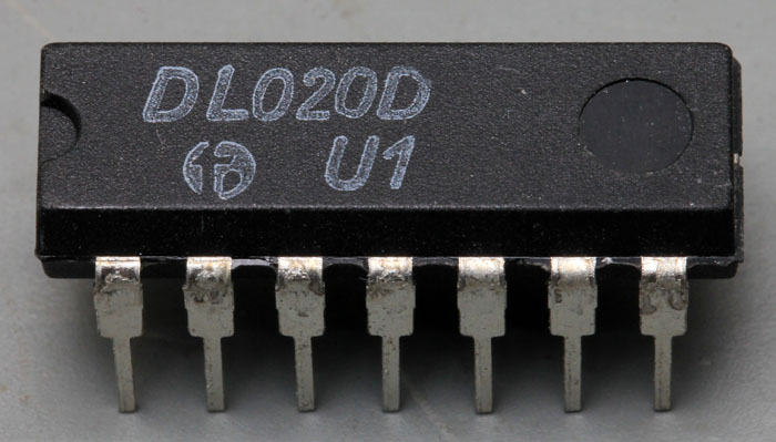
DL020D, a Dual-4-Input-NAND built by the Halbleiterwerk Frankfurt Oder. It´s a 74LS20.

We already had the D220 (https://www.richis-lab.de/wafer01.htm) which is a 7420.

U1 => built in January 1986.
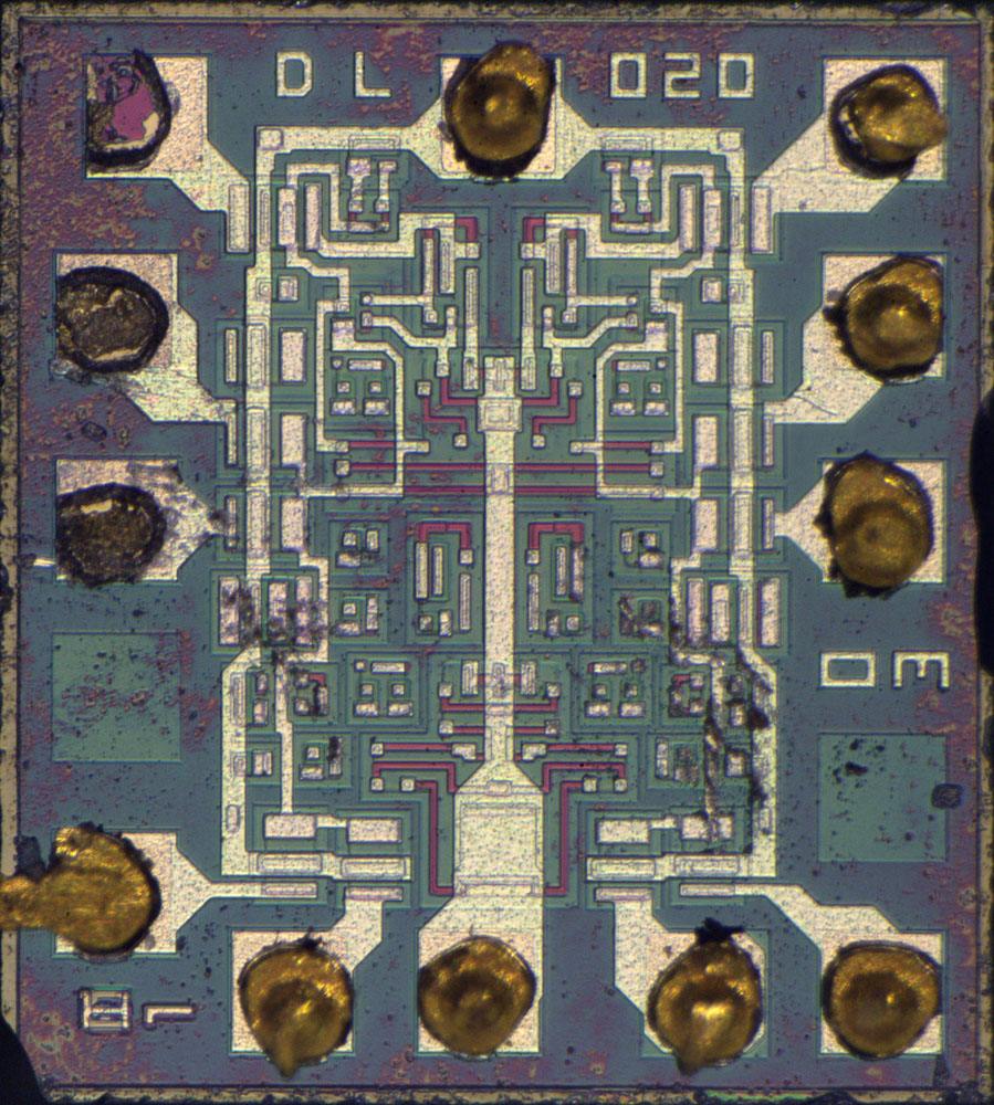


The die is 1,1mm x 1,0mm. The symmetrical design is easy to see and there are a lot of unused parts. I´m sure the design was used for different logic gates by just changing the metal layer.
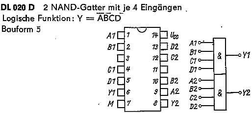
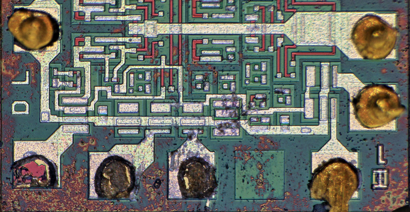
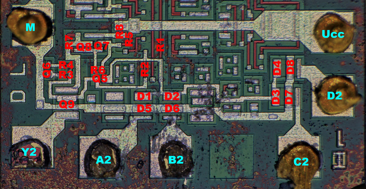
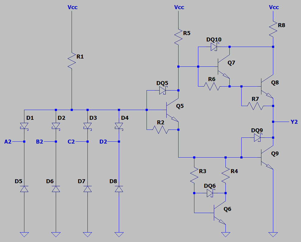


With the background knowledge how a 74LS logic is usually built, we can reconstruct the circuit of the DL020 fairly easily. The diodes D1-D4 isolate the inputs against each other. Since the diodes are in the signal path Schottky diodes are used, which offer fast switching times. The diodes D5-D8 seem to be normal diodes. They protect the DL020 against negative voltages.

If there is no low level at any input resistor, R1 pulls the base of Q5 high. Q5 is a Schottky transistor. A Schottky diode between base and collector ensures that the transistor doesn´t saturate so switch-off is faster. Despite the Schottky diode there is a resistor between base and emitter too. Through this resistor free charge carriers can flow out of the active area.

Around Q5 the potentials are tapped which control the highside and the lowside transistor in the output stage. The highside transistor is a Darlington (Q7/Q8). Q7 is a Schottky transistor which guarantees a fast turn-off. In the place of Q8 a normal transistor is sufficient. Base-emitter resistors are added too (R6/R7). The resistor R8 is necessary, because during switching the lowside and the highside transistor become conductive at the same time for a very short time. During this period the current should be limited.

Q9 is the lowside transistor. Again, this is a Schottky transistor. The network R3/R4/Q6 can be found in a lot of 74LS-logic of other manufacturers. I´m not 100% sure why you need this circuit. I assume the Vbe of Q6 ensures a faster turn-on of Q9. Other suggestions?


The pictures quality could be better but we can identify some parts and structures.

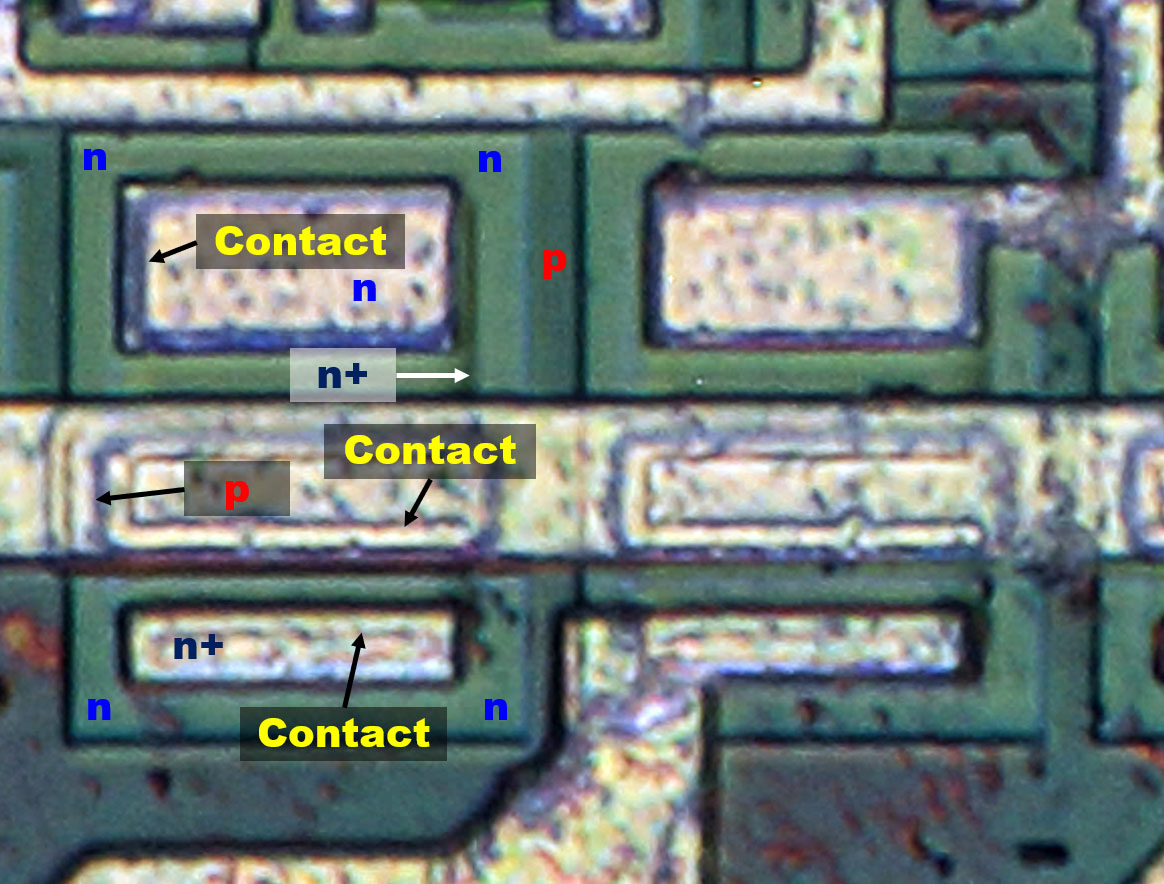
Here you can see two of the input structures, unused on the left side, used on the right side. The input signal is fed from the bottom edge. The horizontal line is connected to GND. The contacts at the upper edge are connected together.

One might expect that this is a transistor but there is no base area visible where two of the three contacts would have to be located. Instead the upper and lower contacts seem to be connected to the n-doped surface. The lower contact is slimmer than the upper one. With the background knowledge that there are usually Schottky diodes at the inputs of a 74LS-logic, these structures are quite argumentative. The lower contact is probably located on a heavily n-doped area which ensures an ohmic contact to the n-doping. Due to the high doping a small contact area is sufficient. The outlines which are barely visible are probably the vias in the insulating silicon oxide. The edges of the heavily n-doped area cannot be seen at the contact. A deeper, strongly n-doped layer conducts charges to the uppermost contact, where the metal layer rests directly on the "normal", weaker n-doped layer. Thus a Schottky diode is formed at the interface. The larger contact area is probably necessary due to the lower conductivity of the weaker n-doped material.

The contact in the middle of the structure is interesting. In most 74LS schematics, there are two Schottky diodes at each input. Here the protection diode seems to be a conventional diode. This can be assumed because another outline can be seen around the outline of the via. A strong n-doping would not serve any useful purpose at this point, it would even act as a low ohmic pull-down resistor. A p-doping on the other hand creates a conventional diode. The conventional diode is slower than a Schottky diode but it probably has advantageous properties in its function as a protection diode. Perhaps it can conduct higher currents in this process.
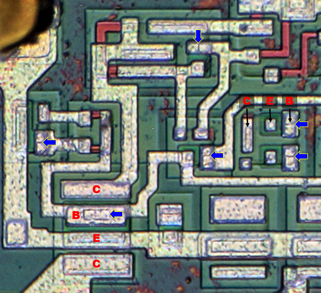


The Schottky transistors can be recognized too. Usually, the structure of a Schottky transistor hardly differs from the structure of a normal transistor. It is sufficient to enlarge the base contact area so it contacts the collector area too. At the contact between the base metal and the collector area the desired Schottky diode is formed. These double contact can be seen even in the smaller transistors of the DL020D. The base contacts are quite large and have an edge where the base and collector regions meet under the metal layer (blue arrows).

In the case of the large lowside transistor in the bottom left corner of the image, a relatively large square can be seen in the area of the base contact. The square is an opening in the base area through which the metal layer can contact the collector area.


https://www.richis-lab.de/logic09.htm

 :-/O
 
The following users thanked this post: SeanB, RoGeorge, schmitt trigger

Online NoopyTopic starter

  • Super Contributor
  • ***
  • Posts: 1725
  • Country: de
    • Richis-Lab
Re: Logic-ICs - die pictures
« Reply #19 on: April 21, 2022, 08:01:49 pm »


Fairchild 9300, a 4Bit shift register.


The die is 2,1mm x 1,6mm.

There are two supply frames surrounding the die. At the lower edges you can see five a little bigger output transistors.


8300?  :-//
Z 6A is probably a mask revision.
In the lower left corner there are some more letters under the metal layer. It looks like 8300 and Z 3A.


https://www.richis-lab.de/logic10.htm

 :-/O
 
The following users thanked this post: SeanB, RoGeorge, capt bullshot

Online NoopyTopic starter

  • Super Contributor
  • ***
  • Posts: 1725
  • Country: de
    • Richis-Lab
Re: Logic-ICs - die pictures
« Reply #20 on: April 24, 2022, 05:34:26 pm »


I didn´t honor the 9300 enough!

The 9300 is one of the 9000 TTL logic Fairchild had invented. With the 9300 familiy Fairchild had an advantage over Texas Instruments. With the MSI (medium scale integration) of the 9300 familiy Fairchild was able to integrate more complex functions in one chip.

Later Texas Instruments outperformed Fairchild and today everybody knows the 74-family...
 
The following users thanked this post: SeanB

Online NoopyTopic starter

  • Super Contributor
  • ***
  • Posts: 1725
  • Country: de
    • Richis-Lab
Re: Logic-ICs - die pictures
« Reply #21 on: April 29, 2022, 08:34:11 pm »


К155ЛA3 (K155LA3) a soviet SN7400: 4x 2-Input NAND

They used the brown mold compound you often see with soviet ICs. It´s a little darker than the mold compound of the KR597SA1 (https://www.richis-lab.de/Opamp25.htm). They sometimes had problems with light entering the package and influencing the integrated circuit.


The edge length is 1mm.


There are some squares to check the alignment of the masks.

And there are three characters. Probably ЛA3?  :-//


At the input transistor there are some options but a lot less than in the DL020 (https://www.richis-lab.de/logic09.htm).


https://www.richis-lab.de/logic11.htm

 :-/O
« Last Edit: April 29, 2022, 08:55:19 pm by Noopy »
 
The following users thanked this post: SeanB, RoGeorge

Online NoopyTopic starter

  • Super Contributor
  • ***
  • Posts: 1725
  • Country: de
    • Richis-Lab
Re: Logic-ICs - die pictures
« Reply #22 on: May 02, 2022, 07:43:19 pm »

Just a small Update to the К155ЛA3 (K155LA3) :


There is a datasheet showing the schematic of the K115 chips.


I have added "names" to the bondpads.


https://www.richis-lab.de/logic11.htm

 :-/O
 
The following users thanked this post: SeanB, exe, RoGeorge

Online NoopyTopic starter

  • Super Contributor
  • ***
  • Posts: 1725
  • Country: de
    • Richis-Lab
Re: Logic-ICs - die pictures
« Reply #23 on: May 15, 2022, 07:41:25 pm »


D172, a J/K-Master-Slave-Flip-Flop built by the Halbleiterwerk Frankfurt Oder. It´s similar to the SN7472.

LN stands for a production in September 1973 or in November 1979. We will see that it has to be 1979.


Datasheet shows what is inside the D172. Picture quality is... Yes...  ;D


In the "Radio Fernsehen Elektronik" issue 16 / 1977 there is an article about the D172. The text tells us that the D172 was improved. The parts of the circuit were rearranged so it consumes less area. In addition the circuit itself was optimized.

The schematic shown in the RFE shows two differences to the datasheet. In addition to the protection diodes at all I/Os (red), a small auxiliary circuit was integrated (blue), which additionally interlocks the right and left halves of the circuit against each other.


The Texas Instruments datasheet for the SN7472 shows the additional circuit as two AND gates.


The die in the D172 above has an edge length of 1.3mm. In the upper area the name D172 is shown in the metal layer.

A large part of the die is discolored. The component was defective. It is therefore likely that the discoloration was caused by this defect. However, the cause of the defect cannot be narrowed down.


The RFE article contains a black-and-white picture of the updated D172 and there is even a color picture on the front page.

In the lower right corner you can find the symbol of an AND gate, the logo of the "Zentrum für Mikroelektronik Dresden". The RFE article is appropriately written by an employee of the Zentrum für Mikroelektronik Dresden.


Comparing the structures you can see that the design is the same. In the chip shown here just the logo is missing.

Since the RFE article from 1977 describes the design as new, it can be assumed that the chip was produced in 1979 not in 1973.


https://www.richis-lab.de/logic12.htm

 :-/O
 
The following users thanked this post: johnboxall, SeanB, doktor pyta, RoGeorge

Online ataradov

  • Super Contributor
  • ***
  • Posts: 11234
  • Country: us
    • Personal site
Re: Logic-ICs - die pictures
« Reply #24 on: May 16, 2022, 02:58:30 am »
Are you drunk or something?

Capacitors are extremely costly in ICs and are used in highly specialized cases where there is no other option. Why and where would you even want to see capacitors here?

And you can't see the point of  making FPGAs, you just have no clue what is going on. Do you think ASICs happen out of thin air? They are designed and prototyped in FPGAs. Also ASICs are expensive and hard to impossible to update. But again, what it has to do with this thread?
Alex
 
The following users thanked this post: SeanB, Noopy


Share me

Digg  Facebook  SlashDot  Delicious  Technorati  Twitter  Google  Yahoo
Smf