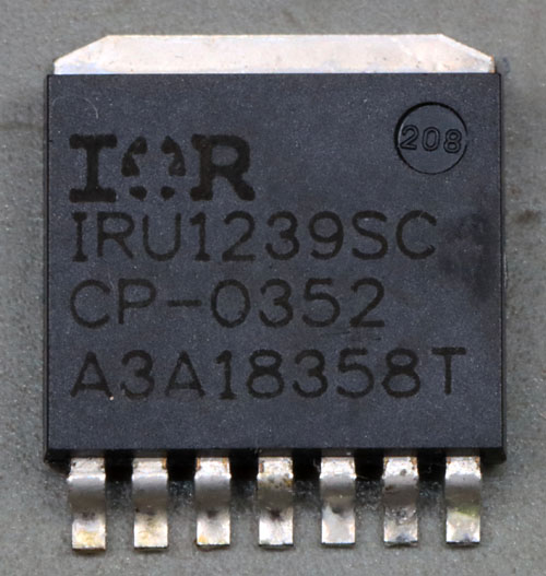
The IRU1239 is a voltage regulator found on Western Digital's WD800BB hard drive.
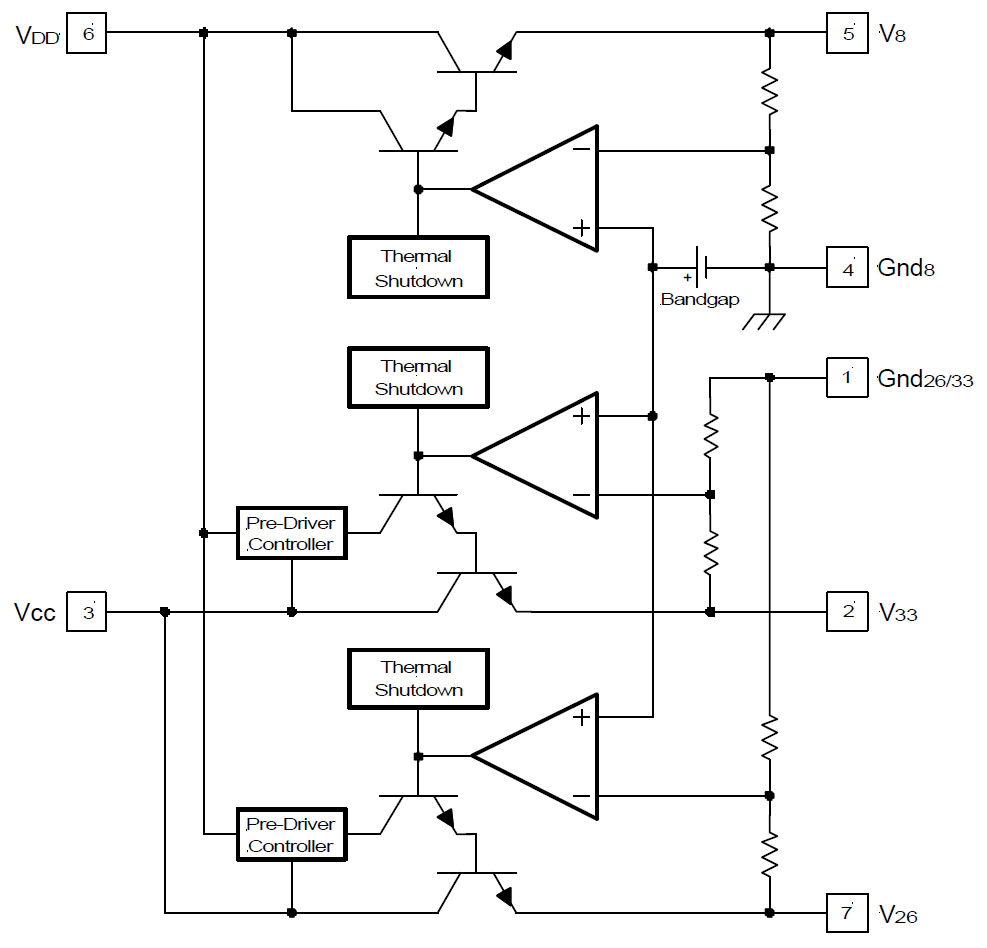
There is no datasheet for the IRU1239. The block diagram above is taken from the datasheet for the IRU1237, which was also developed for use in hard drives and may have a similar design. The IRU1237 contains three voltage regulators with output voltages of 8V, 3,3V, and 2,6V. The current delivery capacity is specified as 0,2A, 1,2A, and 1,2A. The 8V voltage regulator has its own power supply input so that the lower voltage regulators can be supplied with a lower voltage. The lower two voltage regulators also have their own isolated reference potential.
In a Polish forum, the following voltages were measured on the pins of the IRU1239 (pins 1-8) on the WD800BB hard drive: 1.2V / 3.3V / 5.0V IN / 0.0V GND / 1.2V / 12V IN / 2.6V
(
https://www.elektroda.pl/rtvforum/topic367631.html#1876064)
Looking at the IRU1237, the potentials raise a few questions. The IRU1239 would therefore generate a 1,2V potential from the 12V supply. The large difference between the input and output voltage is surprising. If the circuit basically corresponds to the IRU1237, then it could be that the circuit on this channel requires a higher voltage. The other two channels could continue to generate 3,3V and 2,6V from the 5V supply. It would then be questionable whether the measurement at pin 1 was incorrect. It is said there was a voltage of 1,2V on the WD800BB PCB. It is conceivable that they modified the output voltages with this potential at the reference point of the lower voltage divider. A higher potential at the reference point of the voltage divider reduces the output voltage. However, this would mean that the lower voltage regulators normally regulate 4,5V and 3,8V. These would be very unusual voltages. In addition, the IRU1237 requires at least 5,25V to be able to deliver its full output current at 3,3V. For voltages above 3,3V, at least this regulator requires more than 5V at the input.
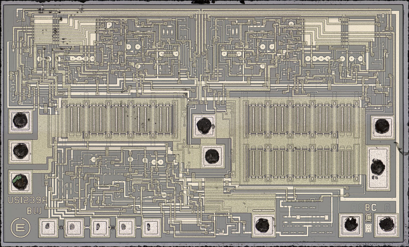
The dimensions of the die contained are 2,2mm x 1,3mm. The designation US1239A is shown in the lower left corner. The letters BW cannot be assigned. In the lower right corner, there are revisions of seven masks. Two metal layers were used.
This image is also available in a higher resolution:
https://www.richis-lab.de/images/vreg/35x03XL.jpg (33MB)
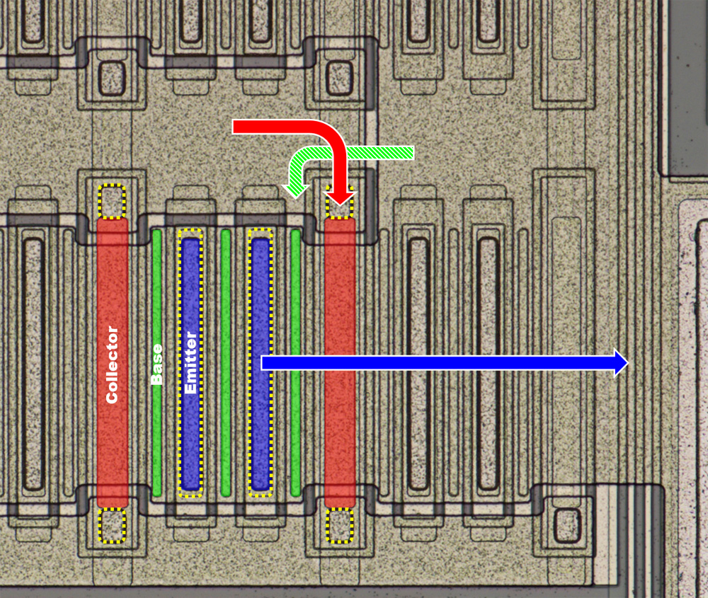
Large power transistors are integrated in the center. The two metal layers enable efficient current conduction. One element of the power transistors consists of two emitters. The elongated contacts are clearly visible (blue). There are strips of the lower metal layer that are connected to the upper metal layer via vias (yellow). From there, the current is conducted to the right via wide lines. The emitter contacts are surrounded by base contacts (green). The base potential of the transistor is connected to the lower metal layer. The base current is supplied within this layer from above and below. The collector current (red) flows in wide strips of the upper metal layer on both sides of the power transistor. Vias provide connections to the lower metal layer, where a strip leads across the collector contact.
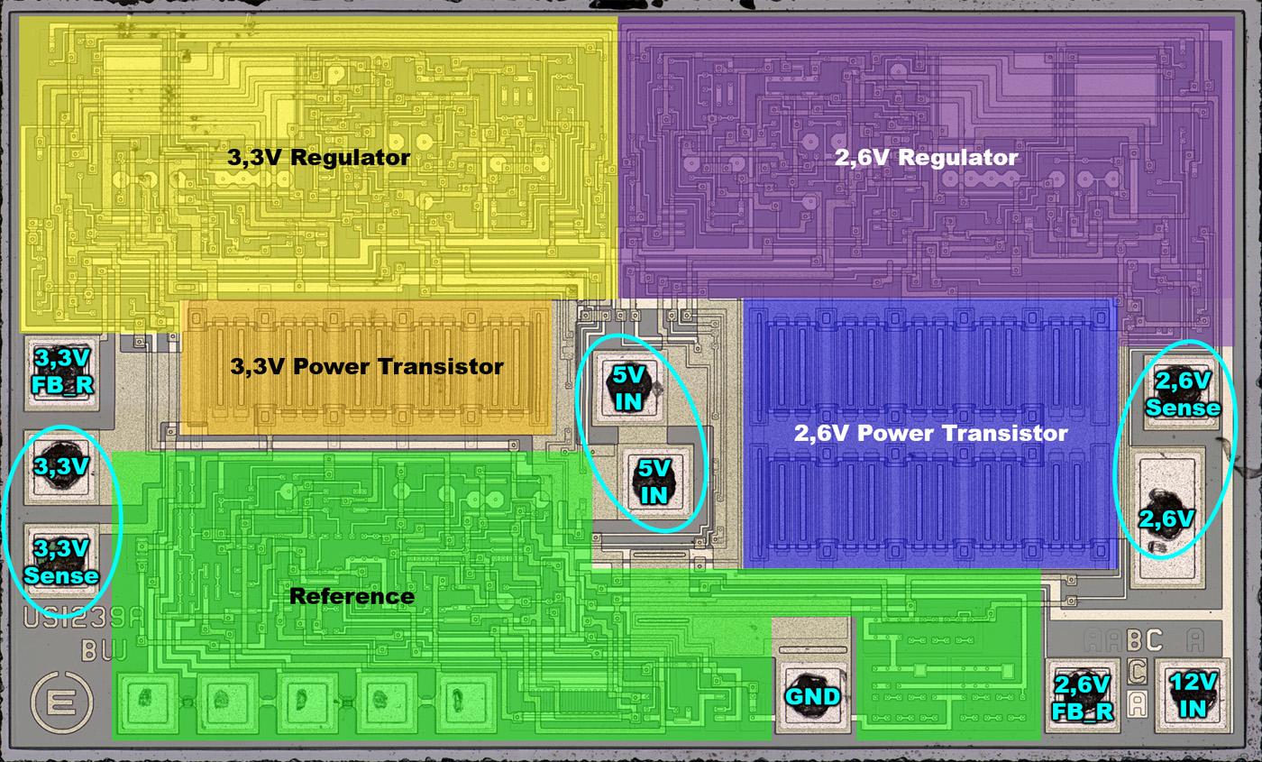
Upon closer inspection and with measurements taken at the pins, the circuit can be reconstructed as follows. The 5V potential enters the circuit in the middle. To the left and right, the current passes through two power transistors. The right transistor is twice as large as the left transistor. These are a 3,3V voltage regulator and a 2,6V voltage regulator. The two regulators are located above their power transistors.
In addition to the actual outputs, each regulator has an input through which it reads back the respective output voltage. The potentials are fed to voltage dividers located in the center of the upper edge. A special feature is the fact that the divided actual voltages are connected with two pins. This also reveals the internal reference voltage with which the regulators operate. This explains the two 1,2V potentials at pins 1 and 5. This is not a third voltage regulator. Presumably, the potentials have been routed to the outside so that the output voltages can be adjusted slightly if necessary.
The reference voltage is generated in the lower section. In the middle of this area you can see the striking transistor combination of a bandgap reference. Fuses on the left offer adjustment options. Both the voltage reference and the regulators use the 12V supply potential.
https://www.richis-lab.de/voltageregulator31.htm 


