Author Topic: Memory - die pictures  (Read 4330 times)

0 Members and 1 Guest are viewing this topic.

Offline NoopyTopic starter

  • Super Contributor
  • ***
  • Posts: 1730
  • Country: de
    • Richis-Lab
Memory - die pictures
« on: September 10, 2021, 03:37:39 am »
Let´s start a new topic for memory die pictures.
At first I wanted to split the topic in RAM and ROM but in my view volatile and non-volatile is more convenient:
https://www.richis-lab.de/RAM.htm
https://www.richis-lab.de/ROM.htm


Today let´s take a look into a FRAM, a Cypress FM24V10 (1MBit).


The die is 3,2 x 2,0mm. There is a huge amount of bondpads. Perhaps you can use the die in a parallel configuration too.  :-/O
You can spot the big uniform memory area divided in eight columns. There is probably some control circuit on the right side of the die.


The structures are tiny but you can spot the year 2008.


The memory itself is way too small to do a deep dive.


https://www.richis-lab.de/RAM01.htm

 :-/O
 
The following users thanked this post: SeanB, daqq, thm_w, Gyro, RoGeorge, Miyuki, james_s, ch_scr, selcuk

Offline RoGeorge

  • Super Contributor
  • ***
  • Posts: 6186
  • Country: ro
Re: Memory - die pictures
« Reply #1 on: September 10, 2021, 08:24:24 am »
Thank you, subscribed!   :)
 
The following users thanked this post: Noopy

Offline NoopyTopic starter

  • Super Contributor
  • ***
  • Posts: 1730
  • Country: de
    • Richis-Lab
Re: Memory - die pictures
« Reply #2 on: September 13, 2021, 08:00:27 am »


HML087, you don´t find very much about this chip. It´s a PROM manufactured by Hughes Electronics and can be found in BMW instrument panels.


The die is 2,9mm x 2,1mm.


HML  :)


Oh it seems to be a HML069. You find the HML069 in some old universal programmer manuals. It´s a PROM that has to be programmed with 12,25V.
There is a 8C in the metal layer and above it is something like 4A or 4H, probably 4A.


Unfortunately layer 3B is quite hard to read that makes it difficult to analyse the circuit.  :-\


Quite some masks: 1A, 2D, 3B, 4A, 5B, 7B, 8C, 11A, 16D


The different crosses allowed them to check the alignment of the masks.


test structures


A big test structure. That´s probably kind of a ring oscillator. There is even a fuse!


Most of the bondpads have the same protection structure.


The output is easy to spot. There is a big highside and a big lowside transistor around it. From the left there comes a differential control signal.
The right bondpad is the high voltage input you need to program the device. It has a different protection circuit.


On the left side of the die there are seven similar looking blocks that get the chipselect and the clock. Three are connected to the line selection. Four are connected to the column selection. That are probably Flip-Flops counting the clock pulses and switching from one memory cell to the other.
Leftmost there are six similar looking blocks connected to the Flip-Flops, probably some support circuit.  :-//


On the right side of the die there are eight similar looking blocks connected to the input bondpad. They are controlled by the circuit in the middle which uses the line selection signals generated on the left side of the die. That is probably the latch for the data input. The output of the latches controls the second part of the line selection circuit.


There is a ninth block locking like the latches. It is not connected to the line selection just to the input signal. There are two lines connected to something on the left side of the die.  :-//


That´s a good picture of the actual memory. There are 16x8 memory cells. On the left side is the output circuit (it´s connected to the output bondpad). On the top there is the column selection. On the right side there is the line selection (read/write) and on the bottom there is some biasing and control circuit.


Every eight columns have one column selection block. Each column selection block consists of a lowside area and a highside area (in the middle) giving you a push-pull driver for every column.


The output circuit is hard to read.  :-//


The line selection is quite complex. On the left side you see four lines going into the memory area (red/green). Every memory line has one red and one green line.
On the right side there is the write circuit. The latches switch the HV or the GND to the red lines.
The green lines are connected to the red lines with the short dark green lines. The yellow transistors are controlled by the line selection generated on the left side of the die.


An overview...


Here we have the memory. It is built out of 2x2 cells. Each cell consists of a floating gate transistor (FG) connected to the red line and a selection gate transistor (SG) connected to the green line that is connected to the output circuit too. A short red line (the "real" red) connects the FG and the SG.


I assume reading a cell is done like this:
The column selection switches a high on the column we want to see. The others are low.
The outer red lines (formerly marked red) are low.
The inner red lines (formerly marked green) are low too except the one we want to select. This one is floating.
The floating gates normally need a mid range voltage to work probably. I assume the high of the column selection is routed to the floating gates by the uppermost line in the lower area. Perhaps the low in the second line is connected to the floating gate line too to get this mid range potential.
Now the combination FG / SG switches the low of the outer red lines to the inner red lines if the floating gate has been programmed active.
I assume the output circuit contains weak pull-ups that are pulled low by the inactive lines. The active line remains high or is pulled low by the FG/SG depending on the data in the FG.
I´m not perfectly sure about that explanation but it seems reasonable.


If you want to write data you just have to select one column no line because you have already eight bit of data in your latches that control all the lines at once.
On the outer red lines (formerly marked red) there is HV if we want to program the FG and a low if we don´t want to.
In the column we want to write the SG is high and with the help of the circuit at the bottom also the FG is high.
The output circuit probably switches a low on the inner red line (formerly marked green).
In this configuration the drain source voltage of the FG transistor is quite high and there is a mid range gate source voltage. The high voltage generates charges by avalanche effects that are attracted to the gate and stored there. This is called "Drain Avalanche Hot-Carrier Injection". That´s not very good for the gate oxide but in a PROM you do that only once.


https://www.richis-lab.de/ROM01.htm

 :-/O
 
The following users thanked this post: SeanB, ch_scr

Offline NoopyTopic starter

  • Super Contributor
  • ***
  • Posts: 1730
  • Country: de
    • Richis-Lab
Re: Memory - die pictures
« Reply #3 on: October 15, 2021, 07:06:19 am »
Well a BBD is also a memory, it´s an anlog memory.
The other BBDs can be found here: https://www.eevblog.com/forum/projects/different-die-pictures/msg3632153/#msg3632153 (and following)
And of course I have listed them here: https://www.richis-lab.de/bbd.htm


Now that should be a Matsushita/Panasonic MN3007. The MN3007 is the PMOS version of the MN3207 (https://www.richis-lab.de/bbd04.htm).


Surprise! That´s not a MN3007 but a MN3207!
Interesting they changed a MN3207 to a MN3007. The MN3207 is completely useless in a circuit designed for the MN3007. It would have been more economic to use any other DIL-8 chip and sell the MN3207 as it is.


Looking at the MN3207 (https://www.eevblog.com/forum/projects/different-die-pictures/msg3672253/#msg3672253) I just found five masks. With the better picture out of the counterfeit MN3007 we know can spot the sixth mask. It seems to be a via in the silicon oxide.


Here you can see the way the MN3207 went. The MN3207 has a pin 1 marking and some kind of a frame.
The MN3007 in the middle has just been ground a little. You can still see the pin 1 marking and the frame except in an area in the upper left corner. There are also some grinding marks.
The right MN3007 has been ground flat. They had to paint it and because of that the pins are black on their shoulders. You can spot grinding marks too.


https://www.richis-lab.de/bbd05.htm

 :-/O
 
The following users thanked this post: SeanB, RoGeorge

Offline NoopyTopic starter

  • Super Contributor
  • ***
  • Posts: 1730
  • Country: de
    • Richis-Lab
Re: Memory - die pictures
« Reply #4 on: November 09, 2021, 09:01:50 pm »


U552C built by VEB Mikroelektronik Karl Marx (what a name  ;D). The U552C is a p-channel EPROM with 2kBit of memory. It is similar to the first EPROM 1702A built by Intel. RD should be the date code for December 1983.
Since the EPROM can be erased with UV light it has a window on top of the package. Here we see the version with a special ceramic window. They did a different version with a quartz glass window. The ceramic window needs nearly three times more light to erase the memory.


Since the U552 is a p-channel EPROM it needs 5V at Ucc and Ubb and -9V at Ugg and Udd to work properly. To write information into the memory you have to decrease Udd to -48V and increase Ubb to 13,2V (max voltages).
CS is chip select. PR makes it possible to write data. P1 and P2 are test inputs.


Udd and Ucc are connected with two bondwires. Ubb is not connected directly but the pin is connected to the area below the die. This special pin is tagged with an arrow on the package.


The die is 3,5mm x 3,2mm. The smallest structures are a little smaller than 10µm so it´s easy to identify and analyze the circuits.


Some markers to check the process quality.


There are five numbers. In GDR the masks were named with letters while numbers showed the revision. It looks like they had to modify one mask eight times!  :-/O


And some test structures!  :-+
This one looks like a normal MOSFET.


Here on the left side, there is another "normal" MOSFET. On the right side there is a MOSFET with a metal gate electrode. Sometimes such MOSFETs with a thick gate oxide are used for ESD protection.


Perhaps a MOSFET with a polysilicon gate but a thick gate oxide?

On the lower edge of the die there is a metal line connected to two testpads so you can check the conductivity of the metal layer.


Hey, some kind of a logo that is integrated in an active structure.  :-+
The S-layer acts as gate electrode for the transistors left and right of the S.


At every input bondpad there is the complementary type of a grounded gate NMOS (ggNMOS). In this MOSFET a parasitic bipolar transistor is conducting whenever an ESD impulse occurs.


On the right side of the die there are two 32x32 memory arrays (white). The address inputs A0-A6 are converted in differential signals (blue). A0-A4 control the column selection between the two memory areas (green). The 2*32 lines are converted to 2*16 to 2*8 to 2*4 (cyan). The address inputs A5-A7 control these switches. The 8 output signals are fed into an inverter stage (orange). If the chip select circuit (pink) is active the inverter stage can control the push-pull output stages (yellow) O1-O6. If you want to write data additional transistors (red) bypass the output stage.
 
The following users thanked this post: SeanB, RoGeorge

Offline NoopyTopic starter

  • Super Contributor
  • ***
  • Posts: 1730
  • Country: de
    • Richis-Lab
Re: Memory - die pictures
« Reply #5 on: November 09, 2021, 09:02:57 pm »


The input/output circuit is relatively complex.


On the right side there are the outputs of the memory lines (L1, L2,...). Here we can see just two of the three multiplex stages (yellow). There is a Pull-up- and a Pull-down-transistor at the output line of the multiplex stage (green). The inverter stage (white) consists of two inverter that share one Pull-Up. The differential output of the inverter stage controls the Push-Pull output stage (blue/red). Between the inverter and the output stage there is the chipselect circuit that is able to drain the current controlling the output stage.
Some transistors used as resistors are controlled by Ugg. The datasheet states that you can toggle Ugg to reduce heat dissipation.


While writing the input pin PR activates the pink transistor that bypasses the output stage to get the input signal at O1 to the multiplexer.


Here we see the amplification stage for the CS signal. The big transistor switches to Udd. In the upper right corner there is a small Pull-Up-transistor.


In the memory array there are horizontal metal lines transferring the information. After four information lines there is one Ucc line.
Vertical polysilicon lines transfer the column signals.


The memory cells are similar to the memory cells in the HML087 (https://www.richis-lab.de/ROM01.htm). Two memory cells share one via to the horizontal line. The active area in the substrate is formed like a grid. The vertical lines distribute Ucc. The horizontal lines are the base for the memory cells.
Every memory cell consists of a control gate and a floating gate. The polysilicon column line activates the control gates. The state of the floating gate controls whether Ucc is connected to the horizontal line or not.
You can put charges into the isolated floating gate by using high voltage. The datasheet specifies 0V at Ucc and -46V to -48V at Udd. The horizontal line and the column line are connected to Udd. With this voltage you generate hot electrons that can travel into the floating gate. As soon as you have charges in the floating gate the memory cell conducts Ucc.
While writing you have to put Ubb to 10,8-13,2V. The positive voltage is necessary to drain the free charges that are generated.
Up to 61,2V, holy shit...  >:D
UV light generates free charges in the whole circuit which allows the charges to drain from the floating gate. Writing and erasing damages the gate oxide. That is why an EPROM is dead after a lot of write cycles.


It works like this: One column is selected which activates the control gates (yellow). Depending on the state of the floating gate Ucc is switched to the horizontal line (green/grey).


Here we see the column selection circuit between the memory blocks. Differential signals generated out of the address inputs A0-A4 are fed from left and right into the circuit.


The opposing columns are connected by the metal layer (yellow). Below the upper memory block there are Pull-Ups (white) that are connected to the column connection line (green).
At the contact of the Pull-Up there is the beginning of an active area that travels to the lower memory block. The horizontal polysilicon lines form transistors (red). Some are shorted by the metal layer. Depending on the potential of the polysilicon one column line is switched to the Udd potential at the bottom of the column selection area.
The active area is splitted at some points (cyan) so the lines next to each other don´t interfere with each other. In addition the uppermost three polysilicon lines do a special job. One column is connected to an area above the first line and the next one is connected between the next two lines which conduct the inverse potential of the first one (blue). These two columns are always isolated from each other.


Address input circuit which generates differential control signals.


There are two test inputs that are connected to a circuit located between the input/output circuit and the memory area. There are two lines of transistors that can switch the horizontal lines to Ucc (red). The first line isn´t connected to any transistor. The other lines are connected alternating but not in an uniform manner. You can´t really switch off half of the memory if you have faulty cells because the other half would be place chaotic in the address area. Strange...
In addition P1 can bypass two floating cells in the first line.


At the bonpad of P1 there is a single memory cell. You can see that the active area is thinner at the floating gate. The control gate is connected to P2.


https://www.richis-lab.de/ROM03.htm

 :-/O

Offline NoopyTopic starter

  • Super Contributor
  • ***
  • Posts: 1730
  • Country: de
    • Richis-Lab
Re: Memory - die pictures
« Reply #6 on: November 19, 2021, 06:43:00 pm »


The MOSTEK MK37092 is a NMOS-Mask-ROM with 8kB of memory. The naming of the memory chips is explained in the datasheet except for the three numbers 092. As we will see later it looks like 092 is the name of the project, more precisely the data that is written into the ROM.


The datasheet shows us the internal setup of the memory.


It looks like the contacts in the package were arranged to perfectly fit to such a memory die.


It seems like half of the die was cut and the lower half was broken to get the die out of the wafer. That was a common procedure.


The die is 5,3mm x 4,8mm.


There are some mask markings on the die. The name of the ROM and the mask revisions can be found in an area which isn´t coated by the passivation layer. The metal looks brighter in this area.
Mask 1 forms the active area. Mask 2X includes some special doping which is necessary to "program" the information into the memory array. We will see that later. The numbers 092 are integrated with this mask so 092 is probably the number of the project. If there is this special doping under the gate of a transistor the threshold voltage is modified. We can´t be sure whether 2X is one mask or there are two masks named 2 and X. One for normal operation (2) and one for the data (X). In the upper picture 2 and X are in two separated squares.
Mask 5 forms the polysilicon. Mask 8 forms the metal layer. Mask 7 seems to generate the vias. I´m not sure about mask 6 perhaps that´s another via, one to contact the polysilicon and one to contact the active area.


There are a lot of test structures on the die. These strings contain small polysilicon stripes connected with the metal layer. I assume that´s for testing the interconnection resistance. I further assume the two long structures left and right of the die and the different spacing is for identifying local process imperfections.


Some transistors with different W/L-factors.


That looks like small parts of the memory area.


On the left side you can measure a stripe of the polysilicon and a stripe of the active area.
On the right side you can contact a normal transistor with a polysilicon gate and a metal gate transistor.


Some more transistors... ...but here there are no contact slots in the passivation layer...  ???


Here we see the structure of the memory area without the metal layer. I will explain how it works later. In the three areas the width of grid structure is different.


The ROM was designed in 1980. The test structures show the resolution of the manufacturing process. Metal layer is a little coarser than the other structures.
 
The following users thanked this post: SeanB

Offline NoopyTopic starter

  • Super Contributor
  • ***
  • Posts: 1730
  • Country: de
    • Richis-Lab
Re: Memory - die pictures
« Reply #7 on: November 19, 2021, 06:44:10 pm »


The memory consists of four blocks (red), each containing 256x64 memory cells. The inner blocks have two, the outer four additional rows that do not contribute to the memory size. However, these are not just dummy structures, which have to ensure a functional core. They partly serve the function of neighboring memory lines.
Most of the address lines arrive from the right. On the right side there are the 12 input buffers too (yellow). The address lines A0, A1, A10 and A11 control a first multiplex column (blue). This column generates 16 control signals for each memory block. Address line A9 doubles the control signals in a second column, so in each memory block 32 lines can be selected (white). In each memory block there are always two lines active.
To select a column in a first step the address lines A2, A3, A5, A6, A7, A8 and A12 in the middle of the die are converted into 128 control signals (black). The address line A4 controls two small output stages at the left end of the memory area. The two output signals of this circuit are connected to the two double lines, which in turn realize the column selection (pink). The address line A4 thus doubles the 128 control signals and only one of the 256 columns of the memory is activated.
At the left output of each memory block, the 64 lines are combined to two outputs (orange). This grouping is possible because only two of the 64 lines are active simultaneously. A mixing of the information cannot occur if you have done the interconnections right.
The output signals of the four memory blocks are fed to two output stages each (light green). The signals pass through another circuit (dark green) which contains the drivers for the output stages.


Here you can see two buffer stages for the address lines. The differential outputs are connected with the first stage of the line selection. The input signals of the corresponding bondpads arrive from above and contact the buffers on the right side. Vertically, four common control lines run through all buffer stages.


The differential signals of the address lines A0, A1, A10 and A11 are connected to eight vertical lines which pass through eight active areas at each of the four memory blocks (red). In these active areas there are two rows of polysilicon gate electrodes. The gate electrodes are placed and contacted in such a way that, depending on the address applied, only one of the 16 outputs in each memory block becomes active. Considering the whole memory, there are four control signals active.
To the left follows the changeover switch, which ensures that 32 line pairs can be selected with the 16 control signals (green). The alternating contacts in the two vertical running control lines are clearly visible. Strictly speaking, this is not a changeover switch. The active areas contain two switches which are supplied by the two vertical lines. By switching the two supply lines, one ensures that just every second active area can switch through the desired signal.


Behind the block with the changeover switches there is another circuit. Probably there are supporting circuit parts, like pull-up or pull-down structures.
The interruption between the inner and the outer memory block is caused by the interconnection circuit at the left side of the memory block. The control on the right side has been mirrored for better signal routing.


After removing the metal layer it becomes more obvious how the line selection circuit is working. Even without a complete analysis it´s clear that there is always one inactive line between the two active lines.
In the right area you can see how the control signals are generated out of the differential address lines. It´s like a NOR circuit. The output is active when none of the transistors is active.


Column selection is performed with the other differential address lines running horizontally in the middle of the die. Similar to the row selection, the lines contact vertically arranged polysilicon strips. Half of the total 14 address lines are located above the wider Vss line in the middle, the other half is located below it. Depending on the contacting of the polysilicon strips and the structure of the active area below only one of the 128 control lines is active.
Between the address lines and the memory areas there are two lines each, which can drive the columns. Depending on the status of the address line 4, one of the two lines becomes active and thus one of 256 columns can be selected with the 128 control lines. In the lower and the upper memory blocks always the same column is active.


A closer look does not reveal the function of the column selection right away. Although there are some differences in the structure and contacts, the majority of the structure appears quite uniform.


After removing the metal layer it becomes clearer. At the lower edge of the picture small part of the column selection circuit is shown. There are small vertical polysilicon strips which are connected partly at the upper partly at the lower end with one of the address lines. The active transistors connect the columns to Vss until the address of the column is selected, thus disabling all transistors. Above the address lines is a pull-up structure.
The two rows of column selection circuits are basically the same. The lower area of the upper row and the upper area of the lower row are just extended a little so the necessary interconnections could be made.
 
The following users thanked this post: SeanB

Offline NoopyTopic starter

  • Super Contributor
  • ***
  • Posts: 1730
  • Country: de
    • Richis-Lab
Re: Memory - die pictures
« Reply #8 on: November 19, 2021, 06:45:15 pm »


The structures in the memory area do not reveal anything about the programming. The metal layer is connected to the active area at regular intervals. Two polysilicon lines of the column selection run between each of the vias.


The functionality becomes clearer as soon as the metal layer is removed. The memory is based on a diagonal grid of the active area. The polysilicon lines run above this grid. In the lower picture they are marked with straight stripes. In fact, they run in a curved pattern as you can seen in the test structures. The polysilicon strips form transistors in the diagonal connections between the crossing points. In the crossing points, the metal layer contacts the active region.
There are always two rows active (green) with one inactive row in between. Actually at the lower end of the memory area there are three lines active. I have ignored this here for better understanding. Each memory line needs two adjacent lines to do it´s job properly. This explains a lot of the dummy lines. They do not directly contribute to the usable memory. Parallel to the two active rows, one of the columns is active (green). The active polysilicon line can activate two of the diagonal transistors at each memory cell in the column. An active transistor causes the potential of the active row to be pulled to the potential of the neighboring inactive rows (bottom row). The desired information is introduced into the memory area by adding an additional doping. If one changes the doping in the diagonal transistors (blue) they never become conductive. The selected row is not affected and delivers a high level to the output (upper row).


After removing the polysilicon there are just the outlines of the active areas left. The doping that represents the programming is not visible. Even in a sharper image it would not stand out. However apparently there are special chemicals that can be used to make different dopants visible.


At the left end of the column selection you can see the buffer stages that realize the switching of the two column driver lines for the upper and the lower memory area.


Left of the memory area the rows are interconnected in a circuit with two columns. The circuit outputs two differential output signals from each of the four memory blocks. Since only two rows are active in each memory block the circuit does not require any additional control. The rows simply need to be alternately connected to one of the outputs.
Left of the interconnection circuit there is a circuit section that most likely takes the output signal of the memory, does some signal conditioning and switching (OE) and drives the output stage. Each output has a large lowside and a large highside transistor placed directly at the bondpad.


The bondwire leading to the bottom of the ceramic package is connected to the substrate, to a frame structure and to a circuit. Perhaps the circuit generates a negative voltage that is supplied to the substrate. A negative substrate gives you better transistor performance. We have seen such circuits on the die of the NEC µPD7220 (https://www.richis-lab.de/GraKa02.htm)


In the upper left corner of the die there is a preparation for an additional bondpad. Just the metal layer is missing. Probably you can use the die in a different configuration as well.
We can take a closer look at the input protection. The bondpad is connected to a resistor strip. The reddish frame overlaps the end of the resistor strip. The frame carries the presumably negative substrate potential. The overlapping area most likely forms a diode that limits negative input voltages.
The seemingly unnecessarily long and wide metal line from the bondpad to the resistor strip forms a transistor with the structures underneath. The resistor strip runs parallel to an active area. In the event of an overvoltage the gate-source voltage of the transistor is high enough to establish a conductive channel between the resistor and the active area under the metal electrode. That´s the protection path for overvoltages.


https://www.richis-lab.de/ROM02.htm

 :-/O
 
The following users thanked this post: RoGeorge

Offline NoopyTopic starter

  • Super Contributor
  • ***
  • Posts: 1730
  • Country: de
    • Richis-Lab
Re: Memory - die pictures
« Reply #9 on: November 22, 2021, 05:01:24 am »
https://www.richis-lab.de/ROM03.htm

Some more pictures to get the memory cell structure of the U552 clearer.  :-/O


After removing the passivation layer and the metal layer the areas under the metal remains opaque and must be dissolved with the underlying silicon oxide layer. In the process, however, the polysilicon strips are also gradually removed. So you have to be careful with the HF.
You can see the active layer under the memory cell pairs narrows towards the central contact. In the narrower region there is the isolated floating gate. Towards the Ucc distribution the control gate activates all memory cells belonging to the column. In these pictures you can see that the Ucc distribution in the active layer does not extend through the complete memory block but is interrupted every eight rows.


The active areas are p-doped (red). Just under the polysilicon gate electrodes (green) the n-doping of the substrate (blue) is still present. In the center, the metal layer contacts the memory cell pair (purple/black).


When programming a memory cell, -47V are applied to the associated row and column line. The control gate thus creates a conductive channel. The potential of the row line causes a charge shift in the floating gate. The high voltage is sufficient to create a conductive channel under the floating gate as well and a current flows. On the left, the potential of the control gate is fixed at 0V, so no conductive channel can be formed underneath.
As the active region narrows in front of the floating gate the current density increases. The high current density generates a large number of free charge carriers. Some of the charge carriers are drained through the active region. The negative charges are more mobile than the positive ones. Some of them spread out in the substrate and must be drained there (12V). However, a certain part of the charges penetrate the thin gate oxide of the floating gate and is trapped there.
From now on, the negative charges deposited in the floating gate ensure that a conductive channel remains under the floating gate. If the associated column is activated, the row line is connected to the Ucc potential.
 
The following users thanked this post: SeanB, Tjuurko, RoGeorge

Offline NoopyTopic starter

  • Super Contributor
  • ***
  • Posts: 1730
  • Country: de
    • Richis-Lab
Re: Memory - die pictures
« Reply #10 on: April 16, 2022, 03:49:58 am »


Tesla MHB4164, a 64kBit-DRAM built by Tesla.


The die is 7,0mm x 3,4mm.


Hey, the IC is a U2164, a 64kBit-DRAM developed by the "Zentrum für Mikroelektronik Dresden"!  :) I don´t know for what the 5 stands for.  :-//

There is an elephant or mammoth. That reminds me of the elephant I have found in the 16kBit-DRAM 4116 built by ITT packaged by Mikroelektronika Botevgrad: https://www.richis-lab.de/prawez06.htm#Elefant
Is there a connection? Or is it normal to put an elephant in an DRAM?  ;D


To understand how the U2164 works it helps to first take a look at the block diagram of the U256. The U2164 is based on this 16kBit DRAM.

The signals RAS, CAS and WRITE control three clock generators which are linked in a way that the necessary functions are started at the right time.

The 7 address lines are routed to a multiplexer for row or column selection. The row decoder generates 128 control signals out of the 7 address lines, which allow to select one row of the memory area.

The memory consists of two 8kBit areas. Each 8kBit area contains 64 rows and 128 columns. In addition to the 128 rows used to store data, each 8kBit area contains a row of 128 dummy cells. The dummy cells provide reference values for the readout amplifiers.

According to the datasheet, the refresh circuit is integrated in the center of the memory area with the readout amplifiers. After a line has been read, its information is no longer available in the memory and must be written to the memory cells again. This task is performed by the refresh circuit. However, the charge stored in the integrated capacitors also ages due to leakage currents. For this reason, the complete content of the memory must be refreshed once every 2ms at the latest.

Although only a single memory cell of the DRAM is addressed, there is alwayse a complete row read out. The column decoder uses only 6 Bits, so there are always 2 of the 128 columns active at the same time. The selection which data should be routed to the output is done outside the memory area via Bit 7. Writing data follows the same pattern.


The block diagram in the datasheet of the U2164 shows that the structures of the U256 were integrated four times. In the center there are 64 sense amplifiers for each 8kBit matrix. The decoders in the columns between the 8kBit blocks activate one row in each matrix. Thus the memory area provides a total of four data lines, one of which is selected by address bit 7. One bit is sufficient here because it can be used twice by row and column selection.

The U256 requires a +12V, a +5V and a -5V supply. With the U2164 a +5V supply is sufficient. The device itself generates a negative voltage for the substrate.


In the "Radio Fernsehen Elektronik" 08/1989 there is a detailed article about the U2164. Also the die is shown, which seems to correspond to the die in the MHB4164. According to the "RFE", more than 140,000 transistors were integrated.


Most of the function blocks can be identified on the die. The 8k memory areas (green) consist of 65 columns and 130 rows. RFE explains that one column and one row serve as a reserve to increase the yield. If individual cells are faulty, these areas can be integrated into the memory. One row provides the dummy cells necessary to effectively read the memory cells. At the top and bottom outer edges are most likely the circuits that precharge the bit lines and the dummy cells with the reference level (blue).

Between the memory blocks is the row selector (red), which takes seven adress lines and activates one of the 128 rows. The memory areas output 64 signals each, which are processed by 64 sense amplifiers (pink). In addition the sense amplifiers write back the active line completely. This line must then be refreshed again after 2ms. The column decoder (purple) selects one of the columns. This results in a total of four active cells. The circuit for selecting a single cell out of the four is not directly visible.

At the left edge is the push-pull output stage (orange) and the circuit to generate the negative substrate voltage (cyan). On the right edge, you can see the analog multiplexer that switches the address lines back and forth between row and column selection (yellow). Two areas contain 16 and 18 equally spaced, relatively large elements (black). They probably are buffer and driver for the row and column selection, input and output data.


...

 
The following users thanked this post: SeanB, Tjuurko, RoGeorge

Offline NoopyTopic starter

  • Super Contributor
  • ***
  • Posts: 1730
  • Country: de
    • Richis-Lab
Re: Memory - die pictures
« Reply #11 on: April 16, 2022, 03:51:05 am »


The structure of the memory cells is described in detail in the RFE article. According to this, a memory cell contains a storage capacity of 50fF. This is the classic DRAM structure with one capacitor and one selection transistor. The article also shows the actual structure of the memory cells. One bit line, represented by the metal layer, always serves two memory cells. Polysilicon layer 2 simultaneously maps the word lines and the gate electrodes of the select transistors. Polysilicon layer 1 forms a relatively large area that serves as a capacitor.

The memory area actually contains not 64 but 128 columns. Each sense amplifier is connected to two adjacent columns and evaluates the difference between the columns. The arrangement of the memory cells ensures that when two columns are active, one column contains the desired information while the other column provides the reference value of the associated dummy cell. This type of differential evaluation with the reference value of a dummy cell is common in such memories.

Splitting the columns in such a way that the two active columns are directly next to each other additionally reduces the soft error rate. This describes the number of sporadic data errors that are not due to hardware errors. The main causes are alpha emitters in the package material, cosmic radiation and neutron radiation. Even small amounts of ionizing radiation can create a current flow that leads to loss of information. The paralleled lines of data and reference signal increase the probability that ionization will affect both lines equally and the information will be preserved.


In total, each memory area contains 130 rows and 130 columns.


How exactly reserve rows and columns could be activated remains unclear. For this, defective areas must be disconnected and reserve areas must be integrated into the circuit.  :-//

There are sections at the edges of the memory blocks that could be suitable for interruption with a laser. Whether a separation would really have taken place in this way remains open.  :-//


Here we have the adress lines in the column decoder.


Detail of the precharge circuit.


Raw decoder...


Here we have the analog mulitplexer (tilted 90°). At the edge you can see 8 input signals and there are 16 output signals.


The 16 signals are routed to the memory area and to the "8+8+2 latch area".


The circuit for generating the negative substrate potential shows the typical structures for this. The area on the far right could be the oscillator for the charge pump. In the middle, relatively large elements, capacitors and transistors can be seen, which probably represent the actual charge pump.

One could think that the bondpad on the left would be connected to pin 1 of the package. This is where the -5V supply is to be applied on the U256. Here, however, the bondpad is most likely connected to the substrate carrier, just like in the D82720 (https://www.richis-lab.de/GraKa03.htm). Fittingly, no relevant resistor, diode or voltage can be measured at pin 1 of a U2164.

There is a double metal frame enclosing the whole die and contacting it many times. This effectively distributes the negative potential.


In the cutting streets there are test structures. Here is looks like we have three different transistors.


The protective structures at the inputs are also described in the RFE article. A grounded gate NMOS becomes active when the voltage is too low and establishes a conductive path to the GND potential. The series resistance limits the current flow. Voltages up to -2V may nevertheless not be applied for longer than 40ns. It is only a protection against undershoots, which can occur with steep switching edges.

If even lower voltages are present, then the parasitic diodes become conductive. Since this path has no current limiting, such low voltages are not allowed. At very high voltages (RFE specifies 12V) the grounded gate NMOS also becomes conductive and protects the circuit.


Here we have the push-pull output stage and the driver for this stage.


https://www.richis-lab.de/RAM02.htm

 :-/O
 
The following users thanked this post: firehopper, Tjuurko, RoGeorge

Offline NoopyTopic starter

  • Super Contributor
  • ***
  • Posts: 1730
  • Country: de
    • Richis-Lab
Re: Memory - die pictures
« Reply #12 on: January 11, 2023, 08:09:19 pm »


The EDI8832C is an SRAM built by the American manufacturer Electronic Design Inc. The designation EDI8832C120CI reveals how the memory is constructed and which specifications it complies with. EDI is the manufacturer. The first 8 stands for the product group SRAM. The second 8 is the word width and the number 32 is the memory depth, resulting in 32k * 8Bit. The letter C shows that 4T memory cells were used. There are also variants with 6T cells. 120ns is the access time. The last two letters show that it is a ceramic package and that the device is approved for the industrial temperature range.


In the "CMOS Static RAM DATA BOOK" EDI describes the differences between 4T and 6T SRAM cells. While in a 4T cell two transistors with two resistors store a logical value, in a 6T cell this function is performed by two CMOS pairs. The transistors to the right and left of the actual memory cell enable selective addressing of a word line. The biggest disadvantage of 6T cells is the higher area consumption. In addition, there is a somewhat higher access time. An advantage is the lower power requirement compared to a 4T cell.


The block diagram in the datasheet shows the basic operation of the device. However, it is rather a principle representation. The memory array has a size of 256kBit, but just 14 address lines are shown. Six address lines therefore activate four rows. This results in 4096 active columns, which can only be reduced to 16 bits by the remaining eight address lines in this diagram. The control circuit then ensures that reading from the active cells or writing to the cells takes place.


The housing contains a relatively large die. The two supply potentials are connected with two bondwires each. The die attach material is scratched surprisingly severe in the gaps.


The die is covered with a polyimide layer. The thickness of this layer can be seen in the recesses for the bond pads.

M5256B is probably an internal designation. In front of and behind it are some test structures, which make it possible to judge the performance of the manufacturing process.


The dimensions of the die are 8,2 x 4,6mm. On the left are the data IOs. The address lines arrive on the right side of the die. The memory is composed of two areas, which in turn contain two equally structured areas. The wide stripes between these areas probably contain the column selection. The exact function cannot be clarified with absolute certainty because of the polyimide layer.


A strip with test structures is integrated on the right edge of the die.


Each of the four memory areas is contacted on the left side with eight structures that look the same. In detail, you can see that each of these structures contains 16 lines. This indicates that the memory contains 512 lines. The address lines, which were not needed for the column selection, select the desired 8Bit out of these lines.


There is an interesting artefact in the middle of the die. Apparently, the circuit has been overloaded there. The polyimide layer is literally burned out. The location of the damage is surprising. Such high-energy overloads would rather be expected in the area of the inputs/outputs.


https://www.richis-lab.de/RAM03.htm

 :-/O
 
The following users thanked this post: SeanB, Tjuurko, RoGeorge

Offline NoopyTopic starter

  • Super Contributor
  • ***
  • Posts: 1730
  • Country: de
    • Richis-Lab
Re: Memory - die pictures
« Reply #13 on: March 16, 2023, 09:19:41 pm »


The MH74S287 is a PROM built by Tesla with a memory depth of 1024Bit. It is a bipolar Schottky PROM with tristate outputs.


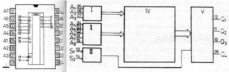
The datasheet shows the basic structure of the MH74S287. The memory (IV) contains 32x32 memory cells. The first address decoder (I) generates eight control signals from the first three address lines, which activate one line each from four memory groups. The second address decoder (II) generates 32 control signals from the remaining five address lines, which activate one of the 32 columns. Thus the contents of four memory cells are transmitted to the output amplifier (V). The output can be controlled by the control signals S1 and S2.


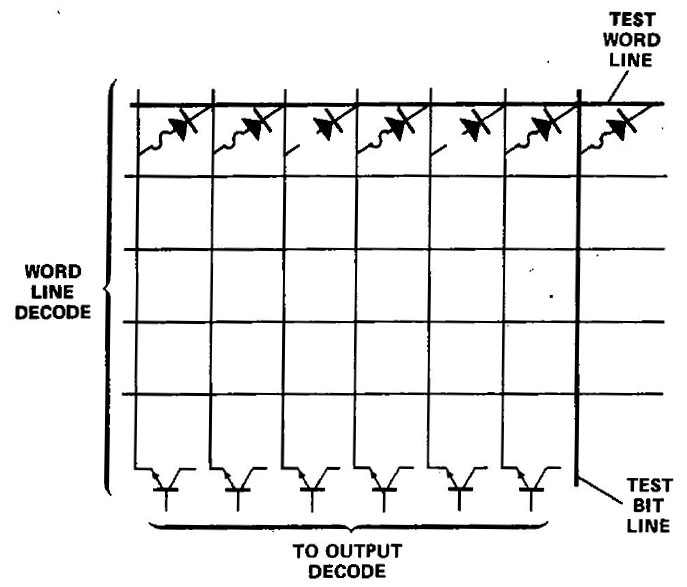
The IEEE paper "A Reliability Assessment of Bipolar PROMs" shows how the memory cells of a bipolar PROM are basically constructed. At the nodes of rows and columns there are fuse elements which are triggered by a current surge during programming. If a row is set to low potential in the circuit shown here, it depends on the state of the fuse element whether the low potential is transferred to the transistor of the respective column. The transistor, which can be activated via its base potential, transfers the state of the active memory cell to the output. The diodes ensure that really only the desired cell is read out and that no unwanted current flows through other areas.

PROMs usually contain a test line and a test column. This is necessary because the functions of a PROM cannot be tested easily after production. If just an unprogrammed matrix exists, it is not even possible to test the selection and sensing circuit. For this reason, a test line and test column are usually integrated, which make it possible to test both writing and reading without influencing the usable area of the memory.


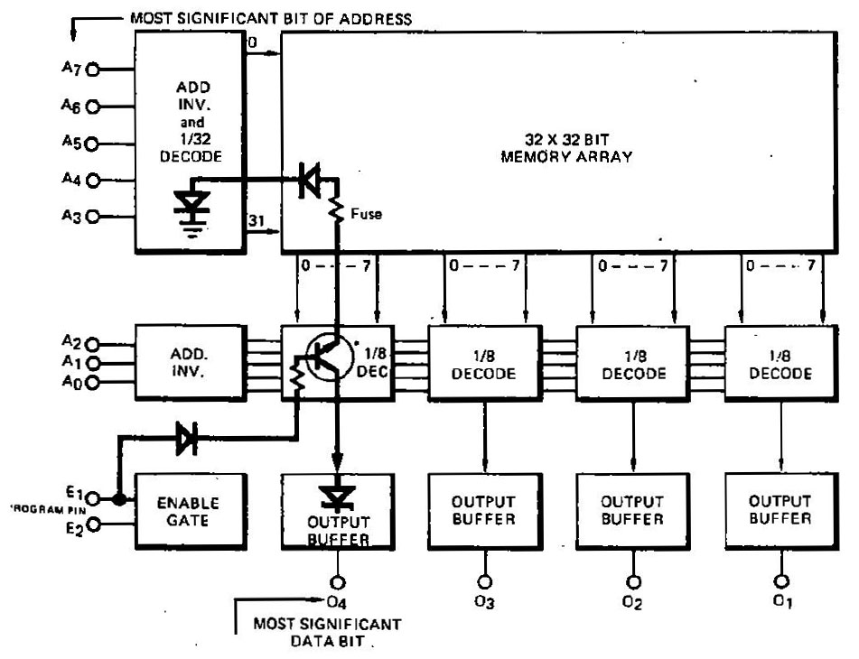
The IEEE article above also provides an overview of the entire circuit of a PROM. The basic design of the PROM shown there is very similar to the MH74S287. However, the MH74S287 works with an inverse logic. Here the address decoder puts one row to ground. The column decoder selects one column each from four groups of 8. When the output is activated, the active transistors pass on the stored information.

Programming is done here by applying a high potential to an enable pin, which triggers the associated fuse element via the transistor in the column selection and the configuration of the row decoder.


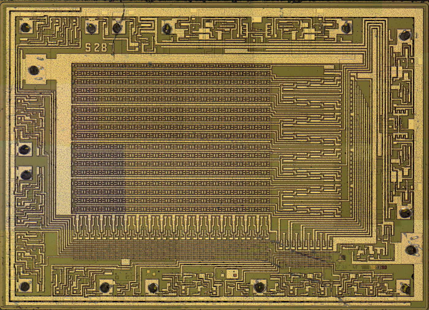
The die of the MH74S287 is 3,6mm x 2,6mm.


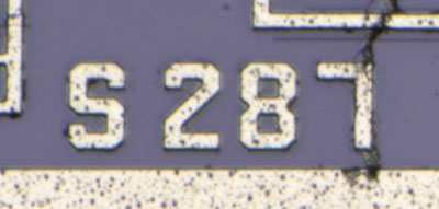
The type designation S287 is shown in the upper left corner of the die.


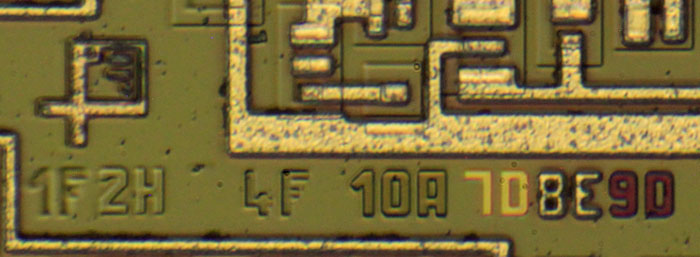
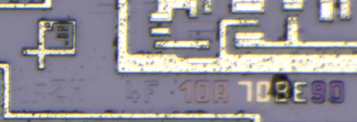
Tesla's logo is shown in the lower right corner. There are also the revisions of seven masks, some of which have been revised very often.


A little further to the left, squares are integrated that allow you to check the alignment of the masks against each other.


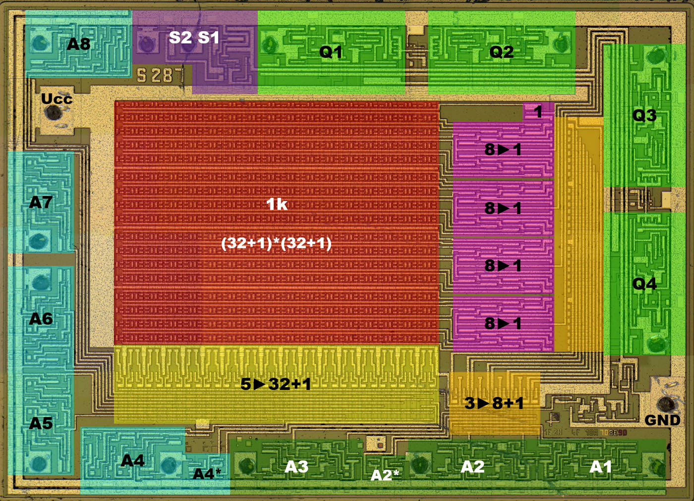
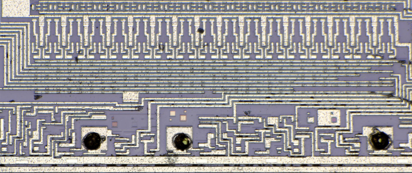
The individual circuit parts are clearly visible on the die. In the center is the 32x32 memory (red), which has an additional test line at the upper edge and an additional test column at the right edge.

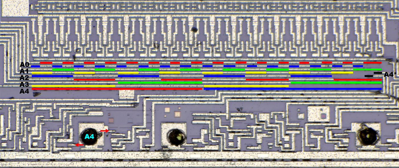
The address lines A4 to A8 are evaluated in the left area (cyan) and fed to the column decoder (yellow) including their complementary values. The column decoder then switches Ucc to one of the 33 columns.

To select one of the 32 columns you already need all five address inputs. To be able to select the test column nevertheless, the address input A4 has been extended with the additional circuit A4*. This is usually a circuit which becomes active only at a voltage which is not present in normal operation. If you want to test the PROM, you apply a slightly higher potential to pin A4 and thus reach the test column.

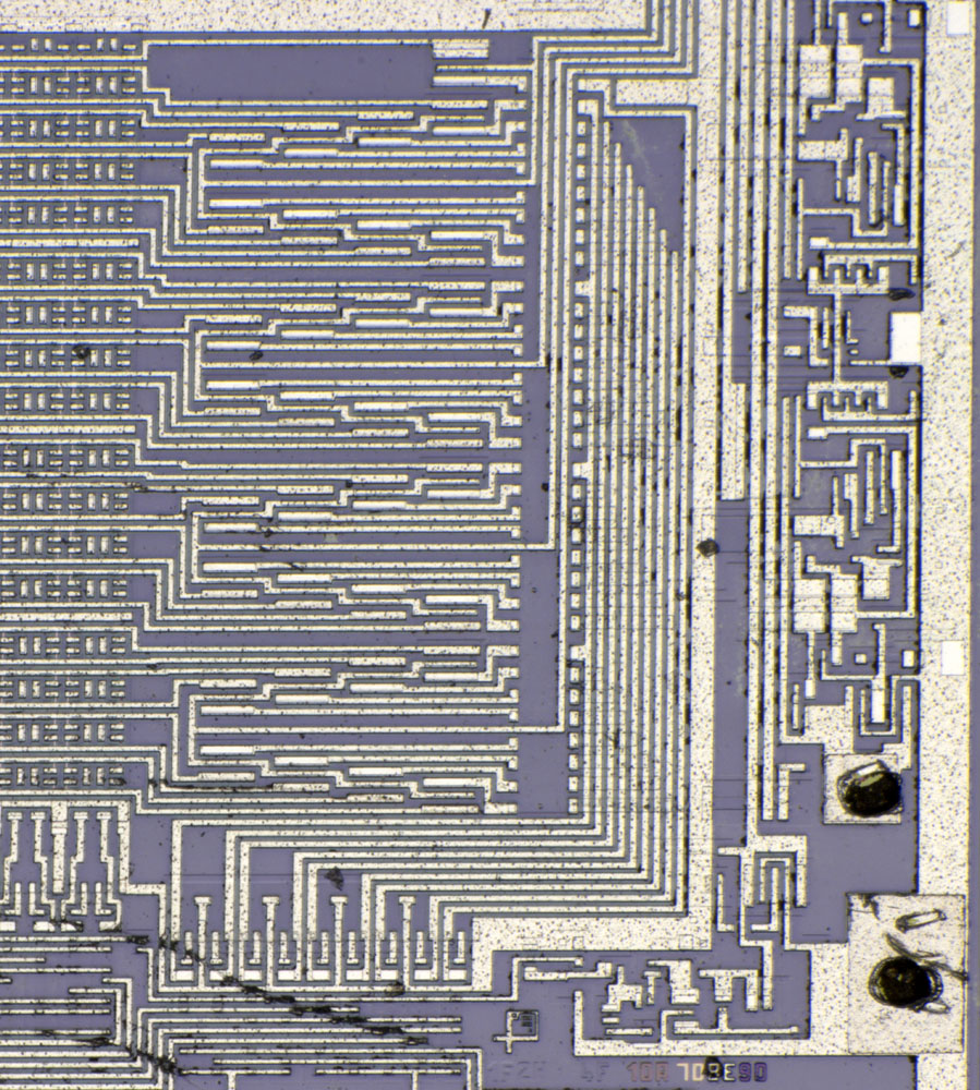
To the signals of the address lines A1 to A3 the complementary potentials are generated too (dark green) and fed to the line decoder (orange). Here the input A2 offers the additional function to activate the test line. The eight control lines of the line decoder are fed to four blocks, where they select and forward one line in each block out of eight lines (pink). The ninth control line connects the test line to output Q1.

The four tristate outputs (green) are arranged in pairs and share a small circuit section. In the upper left area is the enable circuit that activates the outputs (purple).


The memory area is connected to the Vcc potential with very low impedance. Each of the four blocks is flanked by horizontal Vcc lines.


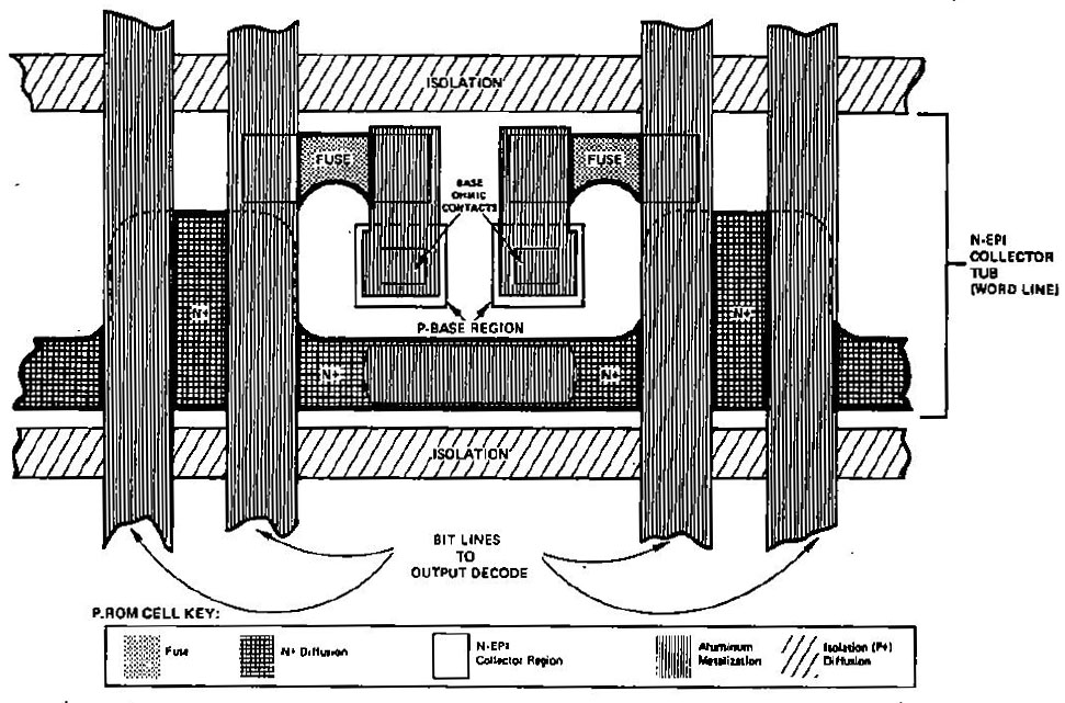
The IEEE article "A Reliability Assessment of Bipolar PROMs" contains a sketch with the typical structure of a bipolar PROM. In this case, the cells are arranged in pairs. The core of the memory cells are the fuse elements, which are usually made of a nickel-chromium alloy. Alternatively, a titanium-tungsten alloy or polysilicon directly has been used. In addition to process-safe manufacturability, low resistance in the intact state and reliably high resistance after the fuse element burns out are important.

In circuit diagrams, base-emitter paths of transistors are often located in series with the fuse elements. Here, there is no emitter. Instead, the base-collector junction has been used as a diode. Below the fuse elements are p-doped squares in the n-doped collector layer. The IEEE article emphasizes the robustness of this implementation. Compared to base-collector diodes, base-emitter junctions are more prone to production defects and failures.

Vertically (horizontally in the MH74S287), the bit lines run in the metal layer. Horizontally (in the MH74S287 vertical) the word lines run, built up with heavily n-doped regions. Between the bit lines, elements of the metal layer reduce the resistance of the word lines. A low-resistance design of these areas but also of the surrounding circuit is important so that a sufficiently high current can flow when the fuse elements are triggered. At the same time, the circuit must also withstand the increased voltage used during programming.


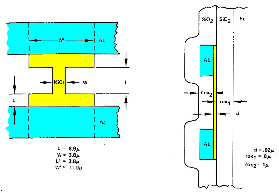
The IEEE article "Reliability Assessment of a Semiconductor Memory by Design Analysis" shows the typical structure of a nickel-chromium fuse. The taper there is 3,8µm wide. This corresponds to the sizes in MH74S287.

Fuses of the metal layer, which are used to adjust integrated circuits, have openings in the passivation layer so that it does not suffer large-scale, undefined damage when the fuse is triggered. This can be seen well, for example, on the die of the LTFLU (https://www.richis-lab.de/REF04.htm#fuse). The fuse elements of a PROM, on the other hand, are located under the passivation layer. This is possible because they are triggered with much less energy.

The amount of energy and the exposure time with which the fuse elements are triggered are critical design parameters. Strips that are not optimally fused can regenerate. The IEEE article explains this effect in more detail. If the fuse does not fuse far enough, a very high electric field is established in the opening. The metal oxides that have formed there can then cause a breakdown despite the low voltage and for the evaluation circuit the fuse appears intact again.


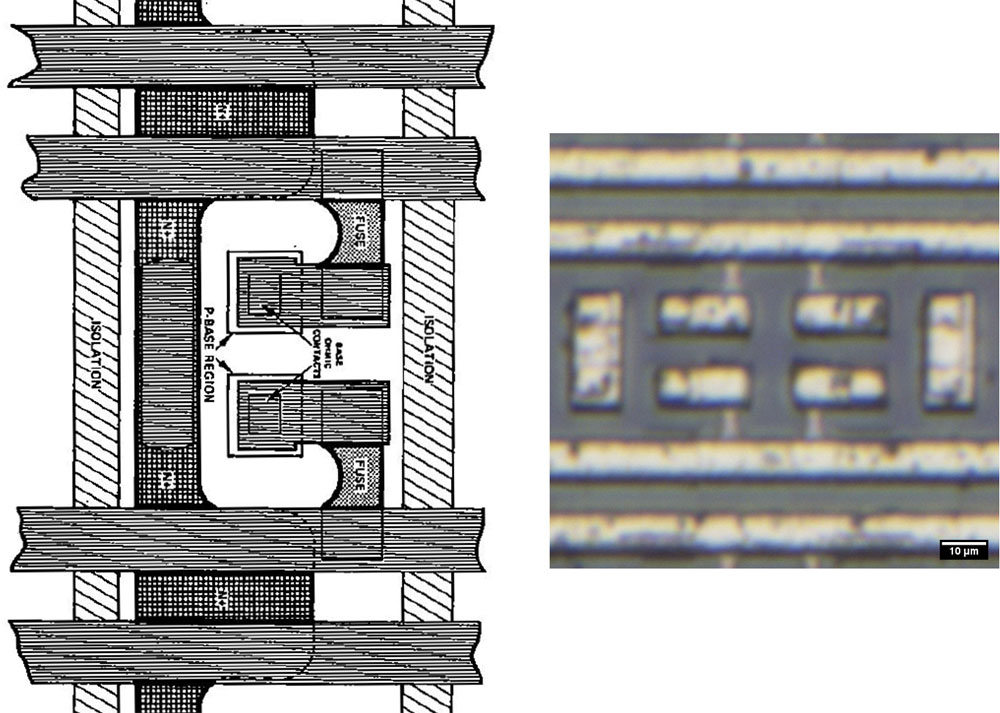
If you compare the sketch from the IEEE article with the memory cells of the MH74S287, you can see that Tesla has always grouped four memory cells together. Otherwise, the structure is apparently the same.

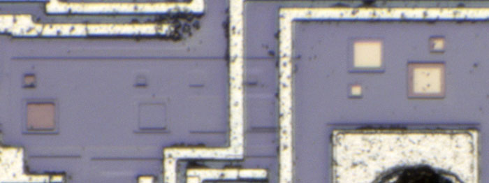
The present device is unprogrammed. You can see the bright fuse elements quite well.


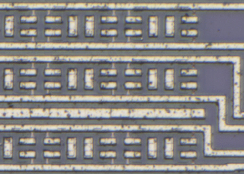
In the test column (far right) you can see how triggered fuse elements look like. The break forms a dark area in the center of the element.


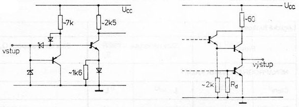
The datasheet shows the input and output circuitry of the MH74S287. Fast Schottky transistors are used there.


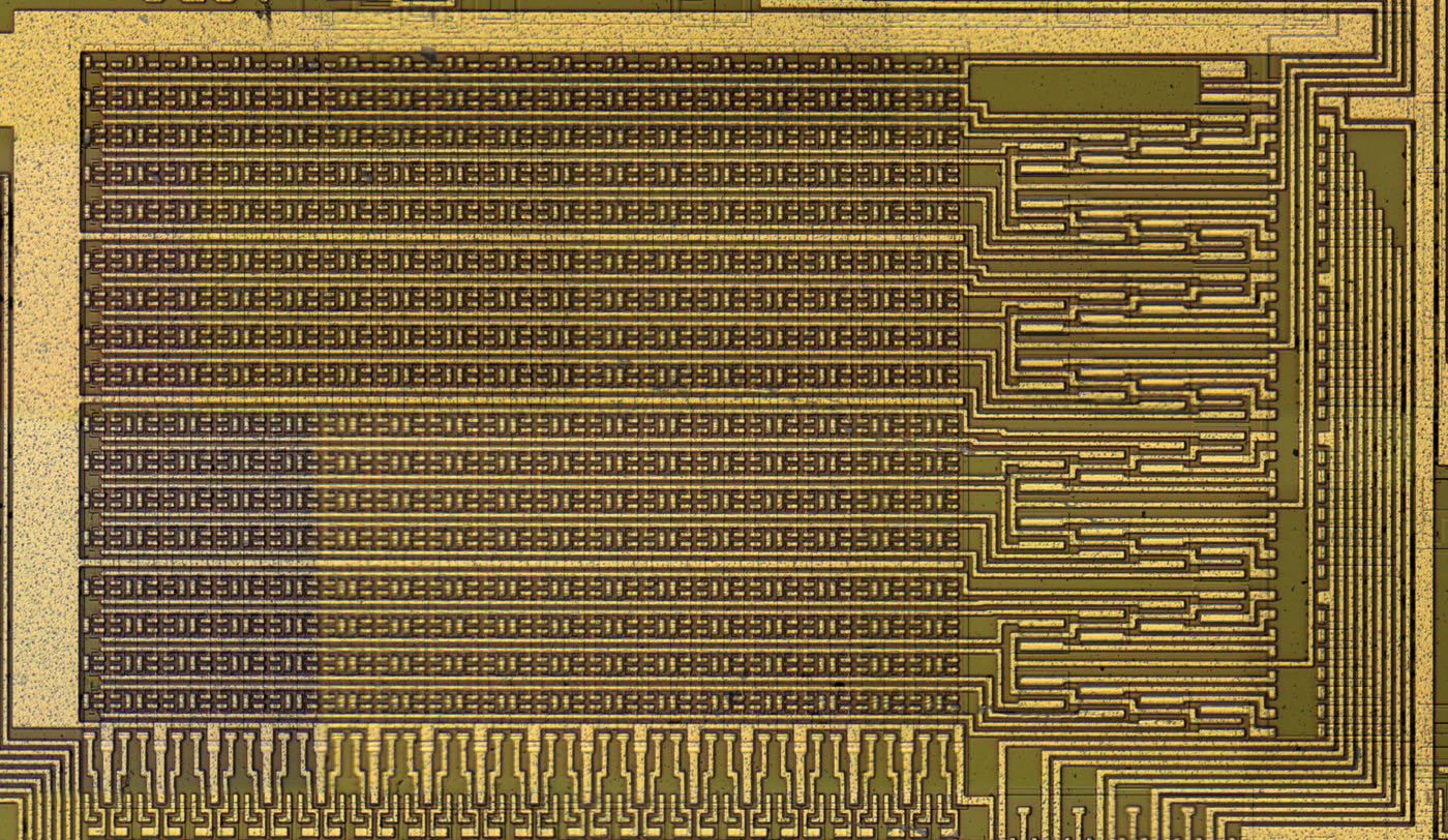
The structure of the column decoder can be seen clearly. The interconnection with the address lines and their complementary lines ensures that each address activates exactly one column. The test column on the far right and the column next to it additionally receive the signals A4*, which are generated in the additional circuit of the address input A4. If the 32nd column is selected and input A4 is in overdrive, the additional circuit ensures that the 32rd column is deactiviated and the 33rd column is activated.


To the right of the column selection is the decoder of the row selection (seen here at the lower edge). This works according to the same pattern and outputs nine control signals.

Eight of the nine control signals pass under the continuing lines at each of the four memory blocks. Each memory block has eight larger transistors, one of which is active. A bus line then leads up from each block and to the four output drivers.

If address input A2 is in overdrive, the control signal in the top block jumps to the single transistor at the top edge and the test line is connected to output driver Q1.

Between the line decoder and the GND bondpad there is a small circuit connected to the two decoders. Presumably a bias generator or something like that.


There is a programming instruction for the MH74S287. According to this, the module must first be supplied with its normal operating voltage. Then you set the address you want to write and apply the pattern to be programmed to the outputs. The outputs are either held at high potential by pull-up resistors or pulled hard to ground.

The programming process is done with an increased voltage of 10V to 11V and is controlled by one of the enable inputs. Before raising the supply voltage, disable the outputs. If the correct voltage is applied, one activates the outputs for 1ms. Where a high current flows, the fuse elements are triggered. The high power dissipation that occurs during this process makes it necessary to define cooling times that depend on how long the increased voltage is applied to the device ("Y").


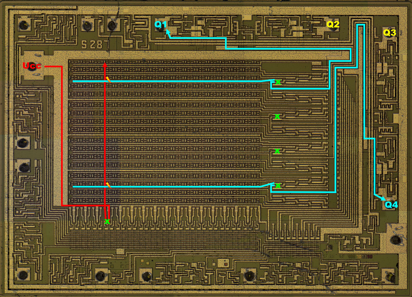
On the die one has tried to make the way the high programming current has to flow as short and low impedance as possible. Ucc is fed directly to the transistors for the column selection. Depending on the state of the address lines, one of the columns becomes active and is supplied with Ucc. On the right side of the memory matrix, one of the rows is switched through in each of the four blocks. Depending on which outputs have a GND potential applied to them, a high current flows across them and the associated fuse elements are triggered.

It is interesting that the output amplifiers seem to be bypassed during programming. From the line selected, a line leads directly to the bondpad via a larger structure. This also explains why a low at the output can be used to disconnect the fuse, but in normal operation a high is present at the output when the fuse is disconnected.


https://www.richis-lab.de/ROM04.htm

 :-/O
 
The following users thanked this post: ale500, RoGeorge

Offline NoopyTopic starter

  • Super Contributor
  • ***
  • Posts: 1730
  • Country: de
    • Richis-Lab
Re: Memory - die pictures
« Reply #14 on: March 29, 2023, 06:57:31 pm »


The AS6C62256 is a 256kBit SRAM built by Alliance Memory. The American company Alliance Memory serves the market for so-called "legacy memory". These are memory chips that are no longer produced by the major manufacturers.


The datasheet shows a block diagram of the AS6C62256 that does not contain any surprising things.


The dimensions of the die are 2,9mm x 1,8mm. The image quality is not optimal, but the typical structure of a memory chip can be seen well.


The details show that the design does not come from Alliance Memory, but was developed by the Taiwanese company Lyontek. The internal designation seems to be LT8012. The B is shown differently and could represent the revision.


The design is from 2004. Above the year you can see some mask designations.


https://www.richis-lab.de/RAM04.htm

 :-/O
 
The following users thanked this post: ale500, RoGeorge

Offline NoopyTopic starter

  • Super Contributor
  • ***
  • Posts: 1730
  • Country: de
    • Richis-Lab
Re: Memory - die pictures
« Reply #15 on: April 20, 2023, 07:07:14 pm »


A cleaned package, so what will we find inside...


The dimensions of the die are only 0,92mm x 0,87mm.


There are a few designations on the die, including the Microchip Technology logo. The strings cannot be recognized very well, but they do not seem to refer to a common product designation.


Even though the structures are very small, some function blocks can be identified. The actual memory area (yellow) has the typical very small and very regular structures. To the left of the memory area is the row selection (purple) and below that the column selection (cyan). The column selection is clearly more complex. Presumably, in the left area actually only a row selection takes place, while below the memory area the signals of the memory cells are evaluated. Writing also requires somewhat more complex circuit parts, since it is done with increased voltages. The charge pump required for this is located at the top edge of the die (red). A clear indication of this are its relatively large capacitors. The remaining areas probably contain the necessary control logic.

The column selection is connected to the memory area by 8*16 lines. In the row selection, one is able to recognize 32 elements. Here, however, it would be quite possible that each element outputs more than one control signal. The memory matrix therefore offers at least 4kBit, maybe more.

The bondpads to supply the circuit can be identified by their more massive connection. This leaves three bondpads as data interface. This speaks for the fact that it is an I²C interface. For Microchip Technology, this is the 24xxyy family. The arrangement of power supply and data interface fits these devices.


In the 24xxyy family there are memories with additional address inputs, but also variants that offer just one write protection pin in addition to the I²C interfaces SDA and SCL. This one here must be such a device. If it really is a 4kBit memory, then this would be the 24xx04. The two middle characters indicate variants that allow different write speeds. Microchip Technology offers memory depths between 128Bit and 2MBit.

The datasheet of the 24AA04 contains a block diagram, which shows the typical circuit parts of an EEPROM. A control logic evaluates the bus signals SDA and SCL. Behind this is a control logic that evaluates the write protection input and controls all areas of the memory. Below this is the voltage generator which generates the increased programming voltage, the row selection and the column selection including signal conditioning. The page buffers allow up to 16B to be transferred before they are written to the EEPROM in one piece.


https://www.richis-lab.de/ROM05.htm

 :-/O
 
The following users thanked this post: ale500, RoGeorge, ch_scr

Offline NoopyTopic starter

  • Super Contributor
  • ***
  • Posts: 1730
  • Country: de
    • Richis-Lab
Re: Memory - die pictures
« Reply #16 on: June 02, 2023, 03:25:32 am »


The T24C02A is an EEPROM with 256B of memory. The manufacturer is the Chinese company Shenzhen First-Rank Technology.

In addition to the T24C02A, the T24CxxA product family offers five larger variants with up to 64kB. Voltages between 1,8V and 5,5V are permissible as supply. At 5V, the maximum clock frequency of the I2C is 1MHz.


The datasheet contains a block diagram showing the usual structure of a serial EEPROM. The T24CxxA memory chips offer additional up to three pins for an address assignment. With the smallest version T24C02A, all three address inputs can be used. The memory then reacts to the address that is assigned to it via these pins, so that up to eight T24C02As can be addressed via one bus.

In the variants with up to 16kB the bits of the external address assignment are partly needed to select one of the pages of the memory. In the two largest variants with 32kB and 64kB, the memory is already addressed via 16 bits and you can use all three address pins as with the T24C02A.


The dimensions of the die are just 0,48mm x 0,42mm. The regular square area represents the memory area, with column and row selections extending upwards and to the right. The large number of squares to the left of the memory could contain the charge pump capacitors whose voltage is used to write into the memory cells.

The bondpads of the supply voltage can be identified due to their massive connection to the frame structures. It is interesting that just three additional bondpads were contacted. This would be sufficient for the serial interface and the write protection. Presumably, the bondpads that are not contacted are the address inputs. In the T24C02A, these should actually be connected to the pins.  :-//


https://www.richis-lab.de/ROM06.htm

 :-/O
 
The following users thanked this post: RoGeorge

Offline NoopyTopic starter

  • Super Contributor
  • ***
  • Posts: 1730
  • Country: de
    • Richis-Lab
Re: Memory - die pictures
« Reply #17 on: January 13, 2024, 09:35:58 am »


The 82S129 is a PROM with a memory volume of 1kBit. The memory cells are based on nickel-chromium elements which are burnt through during programming (see MH74S287: https://www.richis-lab.de/ROM04.htm). The address lines A3-A7 activate one row of a large 32x32 memory matrix. The address lines A0-A2 choose four signals from the 32 output signals of the matrix, which are then output depending on the control signals CE1 and CE2.


The 82S129-PROM is no longer produced. However, there are still applications that use the component. One application is the Sennheiser SK 3063-U pocket transmitter, which is used in television productions, for example. Heart of the transmitter is the TDD1742 frequency synthesiser. An 82S129 PROM defines the frequencies on which the transmitter transmits. A channel selector switch operates four address lines of the PROM, the remaining three address lines are controlled by the synthesiser.


Since the 82S129 PROM is no longer manufactured, Sennheiser now uses a special hybrid in this position. It was not possible to switch to a more modern memory. The pocket transmitters can be switched to other frequency ranges as part of customer service. To do this, the PROM is replaced and memory modules that are compatible with the existing interface are required.

The hybrid module is based on a ceramic carrier, the design of which corresponds to a DIL-16 package. Two resistors and a transistor can be seen on the top. The actual memory is covered by a black encapsulation. There is no further information on this hybrid.


If you remove the potting material, you can take a look at the memory used in the hybrid.


This is obviously a much more modern circuit. The regular structure of the memory area is clearly recognisable. The extensive circuit around the memory area shows that it is most probably an EEPROM. Some capacitors are integrated at the left edge. There is certainly a charge pump there, which generates the higher voltage required to write into the memory cells.


The die shows that the memory was designed by Atmel. The designation 19803 is an internal designation. It can be found in a PCN for the EEPROM AT28C64.

The revisions of eight masks are shown in the lower section. The module uses two metal layers. The upper metal layer obviously cannot be structured as finely as the lower metal layer.


The AT28C64 is an EEPROM with a memory capacity of 8kB. It is therefore 64 times the size of the 82S129. The datasheet contains a block diagram showing the typical structure of an EEPROM.


The transistor is a BC850, an NPN transistor. The potentials are distributed on the ceramic carrier in two layers.


The address lines A0-A7 of the ceramic carrier lead to the respective address lines of the EEPROM. The address lines A8-A12, which the EEPROM also provides, are connected to GND. The address range that could be reached via these adresses is not required. The outputs IO0-IO3 are connected with O1-O4. The outputs IO4-IO7 remain open. Consequently, only the first four bits of the data interface are accessible, but this is sufficient here.

The CE pin of the EEPROM is connected directly to the ground potential. OE is linked to the CE2 potential of the 82S129. WE is connected to the CE1 potential via the transistor, which works as an inverter. In the transmitter circuit, CE1 and CE2 are permanently connected to GND. This could also have been integrated on the ceramic carrier. However, the OE and WE of the EEPROM are connected to the pins to allow the module to be programmed. To do this, a high potential must be applied to CE1 and CE2.


https://www.richis-lab.de/ROM07.htm

 :-/O
 
The following users thanked this post: RoGeorge

Offline NoopyTopic starter

  • Super Contributor
  • ***
  • Posts: 1730
  • Country: de
    • Richis-Lab
Re: Memory - die pictures
« Reply #18 on: March 07, 2024, 02:07:46 pm »


The SEI0181 is a part that was used in arcade game machines made by Seibu. Seibu did not manufacture any semiconductors itself. It is either a free available part which name has been customized or an ASIC that was developed for Seibu. As will be shown, it is an SRAM. The numbers 9050 could be a date code. The component would therefore have been manufactured at the end of 1990.


The die cannot be exposed without damage. The dimensions are 6,4mm x 6,0mm. The image is available in full resolution (63MB): https://www.richis-lab.de/images/RAM/05x02XL.jpg


There are some test structures on the die, but no direct reference to the manufacturer. The test structures in the lower left area of the image show how well the individual masks have been aligned with each other. The numbers 6091 could be an internal project designation. Below these numbers are mask revisions. Of the five Bs, the left-hand B represents the polysilicon layer. Next to it are two metal layers and two masks that generate the connections between the layers.


The structures of the input and output circuits are visible in the frame structure. The interface types can be identified. Inputs are located on the left. Directly behind the bondpads, series resistors limit the input current and thus form part of the protective structures.

There are some outputs on the upper edge. No series resistors have been integrated there. Firstly, the outputs are more robust and secondly, they would have a negative effect on the output level. The left output has only one interface, all other outputs are connected to the rest of the circuit with two lines. The structures under the supply frame are significantly larger for these outputs. They could be tristate outputs. However, it is more likely that these are interfaces that can be used as both outputs and inputs.


The die contains four very similarly structured blocks, each consisting of two memory matrices. In the middle of the die is a logic strip, the exact function of which cannot be worked out easily.


DRAM memory cells, such as those integrated in the Tesla MHB4164 (https://www.richis-lab.de/RAM02.htm), usually only consist of a transistor and a capacitor. They are correspondingly small, but must be recharged regularly so that they don´t lose their information. SRAM cells, on the other hand, retain their information for as long as the memory is supplied with voltage. However, depending on its structure, an SRAM cell typically requires four to six transistors per bit.


From the structures of the memory cells and the control circuits, it can be concluded that each of the eight matrices contains 32x32 memory cells. The module therefore offers a total of 8kBit RAM.

The die has 50 inputs. A simple SRAM requires far fewer inputs. This indicates that it is a dual-port SRAM. With a dual-port SRAM, two function blocks can access the memory at the same time.


The Renesas 70V05 is an example of a dual-port SRAM. The block diagram in the datasheet shows the basic structure of such a device. In addition to two times 8 data pins, the 70V05 has two times 13 address bits and two times 9 control lines.

With the SEI0181, it is noticeable that two times eight data lines are led out of the four blocks and routed to the control logic in the middle of the die. For an ordinary SRAM with an 8-bit wide data bus, the data lines would have been connected directly within these four blocks and selected appropriately. This is not possible with a dual-port SRAM, as one half of the block can be controlled via one interface, while the second interface accesses the second half at the same time.


https://www.richis-lab.de/RAM05.htm

 :-/O
 
The following users thanked this post: RoGeorge, james_s


Share me

Digg  Facebook  SlashDot  Delicious  Technorati  Twitter  Google  Yahoo
Smf